Table of Contents
このサービスマニュアルはエコパルプ
(ECF:無塩素系漂白パルプ)を使用しています。
このサービスマニュアルは大豆油
インクで印刷しています。
This document is printed on chlorine free (ECF) paper with soy ink.
011680
PA
200304-250000
Downloaded from
www.Manualslib.com
DIGITAL MIXING CONSOLE
manuals search engine
SERVICE MANUAL
CONTENTS
(目次)
(総合仕様)
SPECIFICATIONS
DIMENSIONS
(寸法図)
(パネルレイアウト)
(オプションカードの取り付け)
(LSI端子機能表)
LSI PIN DESCRIPTION
IC BLOCK DIAGRAM
(ICブロック図)
CIRCUIT BOARDS
(シート基板図)
(検査)
....................................................... 76/83
(内部設定をMIDI経由で出力(バルクダンプ機能) )
CHECKING THE BATTERY AND THE SYSTEM VERSION
(バッテリーの残量やシステムのバージョンの確認)
(フェーダーのキャリブレーション)
(MIDIデータフォーマット)
(MIDIインプリメンテーションチャート)
BLOCK DIAGRAM
(ブロックダイアグラム)
OVERALL CONNECTOR CIRCUIT DIAGRAM
(総コネクタ接続回路図)
(回路図)
................................................... 4
.......................................................... 12
.................................. 13
(ユニットレイアウト)
(分解手順)
............................ 23
............................................ 32
................................ 33
.................................. 41
....................................... 46
(サービス検査プログラム)
(01V96の初期化)
....................... 114
................................... 119
............................ 134
HAMAMATSU, JAPAN
1.329K-1933
01V96
............... 21
... 90/102
.... 115/117
.......... 119
............... 120
1
Printed in Japan '03.03
Table of Contents

Related Manuals for Yamaha O1V 96


Summary of Contents for Yamaha O1V 96
- Page 1 01V96 DIGITAL MIXING CONSOLE SERVICE MANUAL CONTENTS (目次) (総合仕様) SPECIFICATIONS ........... 4 DIMENSIONS (寸法図) ............12 (パネルレイアウト) PANEL LAYOUT ........13 (ユニットレイアウト) CIRCUIT BOARD LAYOUT ....21 DISASSEMBLY PROCEDURE (分解手順) ......23 INSTALLING AN OPTIONAL CARD (オプションカードの取り付け) ..........32 (LSI端子機能表) LSI PIN DESCRIPTION ........
- Page 2 IMPOR TANT NOTICE This manual has been provided for the use of authorized Yamaha Retailers and their service personnel. It has been assumed that basic service procedures inherent to the industry, and more specifically Yamaha Products, are already known and under- stood by the users, and have therefore not been restated.
- Page 3 01V96 LITHIUM BATTERY HANDLING This product uses a lithium battery for memory back-up. WARNING : Lithium batteries are dangerous because they can be exploded by improper handling. Observe the following pre- cautions when handling or replacing lithium batteries. Leave lithium battery replacement to qualified service personnel. Always replace with batteries of the same type.
-
Page 4: Specifications
01V96 (総合仕様) SPECIFICATIONS General Spec (一般仕様) Number of scene memories Internal 44.1 kHz, 48 kHz, 88.2 kHz, 96 kHz Sampling Frequency Normal rate: 44.1 kHz–10% to 48 kHz+6% External Double rate: 88.2 kHz–10% to 96 kHz+6% fs=48 kHz Less than 1.6 ms CH INPUT to STEREO OUT Signal Delay fs=96 kHz Less than 0.8 ms CH INPUT to STEREO OUT... - Page 5 01V96 Digital Input (2TR IN DIGITAL, ADAT input) Option Input (SLOT) Available cards Optional digital interface cards (MY16, MY8, MY4 series) Input patch — Phase Normal/reverse On/off Gate-type Key in: 12 ch Group (1–12, 13–24, 25–32)/AUX1–8 On/off Comp-type Key in: self /Stereo Link Pre EQ/pre fader/post fader Attenuator –96.0 to +12.0 dB (0.1 dB step)
- Page 6 01V96 24-bit linear, 128-times oversampling (@fs=44.1, 48 kHz), 64-times over- MONITOR OUT DA converter sampling (@fs=88.2, 96 kHz) STEREO, BUS1–8, AUX1–8, DIRECT OUT 1–32, INSERT OUT (CH1–32, Output patch BUS1–8, AUX1–8, STEREO), CASCADE OUT (BUS1–8, AUX 1–8, STEREO, SOLO) OMNI OUT 1–4 24-bit linear, 128-times oversampling (@fs=44.1, 48 kHz), 64-times over- DA converter sampling (@fs=88.2, 96 kHz)
- Page 7 01V96 On/off Comp-type Pre EQ/pre fader/post fader Attenuator –96.0 to +12.0 dB (0.1 dB step) 4-band PEQ On/off AUX1–8 On/off — Fader 100 mm motorized Delay 0–29100 samples Displayed on LCD Metering Peak hold on/off Number of [email protected], 48kHz effects [email protected], 96kHz Bypass On/off...
- Page 8 01V96 Gate Parameters (Gate パラメーター) Threshold –54 dB–0 dB (0.1 dB step) Range –70 dB–0 dB (1 dB step) Attack 0 ms–120 ms (1 ms step) 0.02 ms–1.96 s (216 points) @ 48 kHz 0.02 ms–2.13 s (216 points) @ 44.1 kHz Hold Gate 0.01 ms–981 ms (216 points) @ 96 kHz...
- Page 9 01V96 Threshold –54 dB to 0 dB (0.1 dB step) Ratio (x :1) x=1, 1.1, 1.3, 1.5, 1.7, 2, 2.5, 3, 3.5, 4, 5, 6, 8, 10, 20 (15 points) Out gain –18 dB to 0 dB (0.1 dB step) Width 1 dB–90 dB (1 dB step) Compander H...
-
Page 10: Analog Input Spec
01V96 Analog Input Spec (アナログ入力仕様) Input level Actual Load For Use With Input GAIN Connector Max. Impedance Nominal Nominal Sensitivity before clip –70 dB –60 dB –40 dB –60 dB (0.245 mV) (0.775 mV) (7.75 mV) A: XLR-3-31 type 50–600 Ω INPUT A/B –26 dB –16 dB... -
Page 11: Digital Input Spec
Digital I/O MY8-AE 44.1/48 kHz 24 bit Sampling Rate Con- MY8-AE96S AES/EBU 44.1/48/88.2/96 kHz verter for input MY8-AE96 44.1/48/88.2/96 kHz Yamaha MY4-AD — — 44.1/48 kHz MY8-AD — — 20 bit 44.1/48 kHz ANALOG IN MY8-AD24 —... - Page 12 01V96 Control I/O Spec (コントロールI/O仕様) I/O Port Format Level Connector in Console TO HOST USB 0 V–3.3 V B type USB connector MIDI — DIN Connector 5P MIDI MIDI — DIN Connector 5P THRU MIDI — DIN Connector 5P TTL/75 Ω —...
-
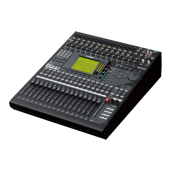
Page 13: Panel Layout
01V96 (パネル レイアウト) PANEL LAYOUT Control Panel (コントロールパネル) AD Input Section (p. 14) SCENE MEMORY Section (p. 17) (ADインプッ トセクシ ョ ン) (シーンメ モリーセクシ ョ ン) CH1-4 CH5-8 CH9-12 PHANTOM +48V Monitor Out DISPLAY ACCESS & Head- INPUT Section (p. 16) (BAL) -10dBV (UNBAL) - Page 14 01V96 AD Input Section (AD インプットセクション) CH1-4 INPUT (BAL) INSERT OUT IN (UNBAL) CH15/16 2TR IN INSERT I/O INSERT I/O INSERT I/O INSERT I/O INSERT I/O NSERT I/O INSERT I/O INSERT I/O INSERT I/O 20dB 20dB 20dB 20dB 20dB 20dB 20dB 20dB 20dB...
- Page 15 01V96 Channel Strip Section (チャンネルモジュールセクション) SOLO q [SEL] buttons (セレクト キー) w [SOLO] buttons (ソロ キー) e [ON] buttons (オン キー) r Channel faders (チャンネルフェーダー) STEREO Section (ステレオセクション) q [SEL] button (セレクト キー) w [ON] button (オン キー) e [STEREO] fader (ステレオ...
- Page 16 01V96 ST IN Section (ステレオ イン セクション) ST IN q [ST IN] button (ステレオ イン キー) w [SEL] buttons (セレクト キー) e [SOLO] buttons (ソロ キー) SOLO SOLO r [ON] buttons (オン キー) t Level controls (レベルコントロール) ST IN 1 ST IN 2 FADER MODE Section (フェーダーモードセクション)...
- Page 17 01V96 Display Section (ディスプレイセクション) OVER STEREO q Display (ディスプレイ) w Stereo meters (ステレオメーター) e Contrast control (コントラスト調節ノブ) r [F1]-[F4] buttons ( [F1]∼[F4]キー) t Left Tab Scroll [ ] button (タブスクロール[ ]キー) y Right Tab Scroll [ ] button (タブスクロール[ ]キー) SELECTED CHANNEL Section (セレクテッドチャンネルセクション)...
- Page 18 01V96 USER DEFINED KEYS Section (ユーザー定義キーセクション) USER DEFINED KEYS q [1]-[8] buttons ( [1]∼[8]キー) Data Entry Section (データエントリーセクション) q Parameter wheel (パラメーターホイール) w [ENTER] button (エンター キー) e [DEC] & [INC] buttons ( [DEC]/[INC]キー) r Left, Right, Up, Down (カーソル 左、右、上、下) (...
- Page 19 01V96 Rear Panel (リアパネル) PHANTOM +48V (p. 19) AD Output Section (p. 19) Digital I/O Section (p. 20) MIDI/Control Section (p. 20) (フ ァンタム+48V) (アナログアウ トプッ トセクシ ョ ン) (デジタル イン/アウ ト セクシ ョ ン) (ミディ/コン トロールセクシ ョ ン) Power Section (p. 20) SLOT Section (p.
- Page 20 01V96 Digital I/O Section (デジタル イン / アウトセクション) q [WORD CLOCK OUT] connector (ワードクロックアウト 端子) w [WORD CLOCK IN] connector (ワードクロックイン 端子) e [ADAT IN/OUT] connectors (ADAT イン / アウト 端子) r [2TR OUT DIGITAL COAXIAL] connector (2 トラックデジタルアウト COAXIAL 端子) t [2TR IN DIGITAL COAXIAL] connector (2 トラックデジタルイン...
-
Page 21: Circuit Board Layout
01V96 (ユニットレイアウト) CIRCUIT BOARD LAYOUT Bottom Assembly (ボトム Ass’ y)MAIN Power Transformer (電源トランス) Downloaded from www.Manualslib.com manuals search engine... -
Page 22
01V96 Control Panel Assembly (コンパネ Ass’ y)
(1/2) (2/2) (1/2) (2/2) Downloaded from www.Manualslib.com manuals search engine... -
Page 23: Disassembly Procedure
01V96 (分解手順) DISASSEMBLY PROCEDURE 注意:作業中は指を挟まない様に注意してください。 Note: Take care not to trap your fingers. After replacing the circuit board or fader of FD, please ※FDシート又はフェーダーを交換後は、 フェーダーのキャ リブレーションを実施してください。 (119 ページ参照) calibrate the faders. (See page 119.) コンパネ Ass'y Control Panel Assembly (所要時間:約 3 分) (Time required: About 3 minutes) 1-1. - Page 24 01V96 Control panel assembly (コンパネAss'y) Stay (ステイ) (WA963600) Bottom assembly (ボトムAss'y) (写真1) Photo.1 Bottom Assembly Section ボトム Ass'y 部 MAIN シート MAIN Circuit Board (所要時間:約 5 分) (Time required: About 5 minutes) 2-1. コンパネ Ass'y を固定します。 (1 項参照) 2-1. Fasten the control panel assembly. (See procedure 1.) 2-2.
-
Page 25
01V96 [220] [221]
[170] Photo.2 (写真2) Photo.4 (写真4) [222] AC shield plate (ACシールド金具) [170] [110] MAIN [130] Power transformer (電源トランス) Lithium Battery (リチウム電池) Battery VN103500 VN103600(Battery holder for VN103500) [290] Notice for back-up battery removal Push the battery as shown in figure, then the battery will pop up. - Page 26 01V96 AC シート AC Circuit Board (所要時間:約 5 分) (Time required: About 5 minutes) 8-1. コンパネ Ass'y を固定します。 (1 項参照) 8-1. Fasten the control panel assembly. (See procedure 1.) 8-2. AC シールド金具を外します。 (6 項参照) 8-2. Remove the AC shield plate. (See procedure 6.) 8-3.
- Page 27 01V96 コンパネ Ass'y 部 Control Panel Assembly Section ※シートを取り外す時に、 ステイでコンパネAss'yを45度 When removing the circuit board, if it is hard to handle while the control panel assembly is fixed slantwise 程度に固定した状態で作業がしにくい場合は、 180度開 いて作業をしてください。 at the stay, open it widely at 180° for the work. ADA シート...
- Page 28 01V96 FD シート FD Circuit Board (所要時間:約 5 分) (Time required: About 5 minutes) 12-1. コントロールパネル面より、フェーダーノブ 17 個 12-1. Remove the seventeen (17) fader knobs from the を外します。 (写真 15) control panel side. (Photo.15) 12-2. コンパネ Ass'y を固定します。 (1 項参照) 12-3.
-
Page 29
01V96
Insulation sheet (絶縁シート) [210] Fader knob Cord holder Cord holder (フェーダーノブ) (インシュロックタイ) [210] (インシュロックタイ) Photo.15 (写真15) [210]: Bind Head Tapping Screw-B (+バインド B タイト) 3.0X8 MFZN2BL (EP600190) Photo.16 (写真16) LCD Circuit Board and LCD LCD シート、液晶ディスプレイ (Time required: About 20 minutes) (所要時間:約... -
Page 30
01V96
LCD shield plate LCD (液晶ディスプレイ) (LCDシールド板) [190B] [60] [100] [60] (+バインド B タイト) (+バインド B タイト) [100]: Bind Head Tapping Screw-B [60]: Bind Head Tapping Screw-B 3.0X8 MFZN2BL (EP600190) 3.0X8 MFZN2BL (EP600190) [190B]: Bind Head Tapping Screw-B (+バインド... -
Page 31
01V96
[450A]: Encoder knob (エンコーダーノブ) [460]: Encoder knob (エンコーダーノブ) [450B]: Encoder knob (エンコーダーノブ) Photo.21 (写真21) Hexagonal nut (特殊六角ナット) [190C] (1/2) (1/2) Encoder angle bracket (エンコーダーアングル) [190D] (2/2) [190C] [190D] Encoder knob (エンコーダーツマミ) [190]: Bind Head Tapping Screw-B (+バインド... -
Page 32: Installing An Optional Card
01V96 (オプションカードの取り付け) INSTALLING AN OPTIONAL CARD Follow the steps below to install an optional mini-YGDAI オプションのmini ‐ YGDAI カードは次のように取り付 card. けます。 1 01V96 の電源がオフになっていることを確認します。 1 Make sure that the power to the 01V96 is turned off. 2 Undo the two fixing screws and remove the slot 2 スロットの固定ネジをゆるめ、スロットカバーを取り... -
Page 33: Lsi Pin Description
01V96 (LSI 端子機能表) LSI PIN DESCRIPTION M37641M8-141FP (X2485200) CPU (USB 32K) ................33 HD6417709SF133 (X2081A00) CPU (SH-3) ................. 34 YSS910-S (XV988A00) DSP6 (Digital Signal Processor) ............35 YSS919B-H (XZ693B00) DSP7 (Digital Signal Processor) ............36 SGH603064F-62F (XV973A00) Gate Array .................. 37 YM3436DK (XG948E00) DIR2 (Digital Format Interface Receiver) ........... - Page 34 01V96 HD6417709SF133 (X2081A00) CPU (SH3) MAIN: IC001 NAME FUNCTION NAME FUNCTION CKE/PTK5 CK enable / Port K Mode control RAS3L/PTJ0 RAS address bus / Port J Vcc(RTC) Power supply +1.8 V PTJ1 Port J XTAL2 CASL/PTJ2 CAS address bus / Port J Crystal oscillator EXTAL2 VssQ...
- Page 35 01V96 YSS910-S (XV988A00) DSP6 (Digital Signal Processor) MAIN: IC301, 302 NAME FUNCTION NAME FUNCTION Power supply (3.3 V) Ground Ground DB13 System master clock input (60 MHz or 30 MHz) DB14 System master clock output (High or 30 MHz) DB15 Vdd5 Power supply (5 V) DB16...
- Page 36 01V96 YSS919B-H (XZ693A00) DSP7 (Digital Signal Processor) MAIN: IC201-204 NAME FUNCTION NAME FUNCTION PLLEN PLL enable input (0: PLL unuse, 1: PLL use) SIO32 /TEST Test mode setting (0: TEST, 1: Normal) SIO33 AVss Analog ground SIO34 PLL filter SIO35 Serial data bus AVdd Power supply (2.5 V)
- Page 37 01V96 SGH603064F-62F (XV973A00) Gate Array MAIN: IC712 NAME FUNCTION NAME FUNCTION Data bus Encoder input Ground Data bus Ground Ground Encoder input Data bus Ground Ground Data bus Ground Encoder input Not used Ground RA10 Encoder input RB10 RA11 RB11 Encoder input Address bus RA12...
- Page 38 01V96 MBCG61594-130 (X3299A00) ATSC2A MAIN: IC401, 457 NAME FUNCTION NAME FUNCTION Power supply +3.3V Power supply +3.3V XTST LSI test pin PB_H_M4_SEL Port B audio data input buffer active select Ground PB_O_MUTE Port B mute WT_X CPU interface write input Ground RD_X CPU interface read input...
- Page 39 01V96 CS8415A-CS (X2089A00) DIR (Digital Audio Interface Receiver) MAIN: IC501 NAME FUNCTION NAME FUNCTION CDOUT Data out (SPI) RXP4 Additional AES3/SPDIF receiver port Control port chip select (SPI) OSCLK Serial audio output bit clock /EMPH Pre-emphasis OLRCK Serial audio output left/right clock RXP0 SDOUT Serial audio output data...
- Page 40 01V96 CS8405A-CS (XZ349A00) DIT (Digital Audio Interface Transmitter) MAIN: IC504 NAME FUNCTION NAME FUNCTION SDA/CDOUT Serial control data I/O (I C) / Data out (SPI) TCBL Transmit channel status block start AD0//CS Address bit 0 (I C) / Control port chip select (SPI) Address bit 2 (I Not used Auxiliary AES3 Receiver port...
-
Page 41: Ic Block Diagram
01V96 (IC ブロック図) IC BLOCK DIAGRAM TC74VHC00F (XT229A00) 74VHC04SJX (XY871A00) 74VHC08SJX (XY872A00) MAIN: IC138 MAIN: IC131, 453 MAIN: IC014, 015, 503 Quad 2 Input NAND Quad 2 Input AND SN74HCU04NSR (XW842A00) ADA: IC007 Hex Inverter TC74VHC14F-EL (XW876A00) TC74VHC74F-EL (XW875A00) HD74HC123AP (IR012310) ADA: IC005 MAIN: IC024, 307, 455 DCA: IC350... - Page 42 01V96 SN74HC273NSR (XH223A00) TC74VHC541F-EL (X3954A00) 74VHC245SJX (XY874A00) MAIN: IC701-706 MAIN: IC117, 209, 505, 603 ADA: IC951, 952 MAIN: IC102-104, 106, 113-116, 132, Octal 3-State Buffer TC74VHC273F (EL) (XY254A00) 506, 507 FD: IC007-010 SN74HC245NSR (XD838A00) Octal D-Type Flip-Flop FD: IC005, 006 MAIN: IC709-711, 713 TC74VHC245F (XT487A00) ADA: IC001, 003...
- Page 43 01V96 MC26LS30DR2 (XL334A00) ADA: IC011 Line Driver SINGLE-ENDED MODE DIFFERENTIAL MODE Inputs Outputs EIA-423 EIA-422 SR-A Operation Mode A B C D A B C D Input A Output A Differential +5.0 SR-A Enable AB (EIA-422-A) Input B/ Output B Input A Out A Out A...
- Page 44 01V96 µPC4570G2 (XF291A00) NJM2904M (XV190A00) TC7SH32FU (TE85L) (XW633A00) FD: IC002 ADA: IC102, 153, 202, 253, 254, 302, MAIN: IC016, 017 353, 354, 402, 453, 454, 502, NJM2904V (TE1) (XR532A00) TC7SET32FU (XW814A00) 602, 702, 802, 902, A02, B02, C02, D02, E02, F02, G02 MAIN: IC004 MAIN: IC022, 451, 458 HA: IC101, 201, 301, 401, 501, 551-553,...
- Page 45 01V96 TLC2932IPWR (XV064A00) MAIN: IC143 LOGIC V PFD INHIBIT VCO INHBIT VCO V VCO OUT SELECT LOGIC V VCO V DETECTOR CHARGE PUMP SELECT BIAS VCO OUT COIN VCO GND VCO INHBIT PFD OUT PFD INHIBIT LOGIC GND LOGIC GND PFD OUT VCO GND COIN...
-
Page 46: Circuit Boards
01V96 (シート基板図) CIRCUIT BOARDS DCCOM (AC) Circuit Board (X3434C0) ........46 DCCOM (DCA 1/5) Circuit Board (X3434C0) ....... 47 DCD Circuit Board (X3858B0) ..........48/49 FD Circuit Board (X3423B0) ............ 50/52 HACOM (ADA) Circuit Board (X3422B0) ......... 54/56 HACOM (HA) Circuit Board (X3422B0) ........58/60 MAIN Circuit Board (X3421B0) ........ - Page 47 01V96 DCCOM (DCA 1/5) Circuit Board to Power Transformer not installed to HA-CN551 to ADA-CN953 to MAIN-CN005 not installed not installed (部品側) Component side 2NAP-V989570-2 (J, U, V models) 2NAP-V989570-2a (H, B, W K models) Downloaded from www.Manualslib.com manuals search engine...
- Page 48 01V96 DCD Circuit Board to MAIN-CN004 not installed to FD-CN002 to Power Component side ( 部品側) Transformer 2NAP-V989580-2 Downloaded from www.Manualslib.com manuals search engine...
- Page 49 01V96 DCD Circuit Board Pattern side (パターン側) 2NAP-V989580-2 Downloaded from www.Manualslib.com manuals search engine...
- Page 50 01V96 to MAIN-CN704 FD Circuit Board 1 fader 2 fader 3 fader 4 fader 5 fader 6 fader 7 fader 8 fader 9 fader 2NAP-V989450-2 Downloaded from www.Manualslib.com manuals search engine...
- Page 51 01V96 to DCD-CN202 10 fader 11 fader 12 fader 13 fader 14 fader 15 fader 16 fader STEREO fader (部品側) Component side 2NAP-V989450-2 Downloaded from www.Manualslib.com manuals search engine...
- Page 52 01V96 to DCD-CN202 FD Circuit Board 2NAP-V989450-3 Downloaded from www.Manualslib.com manuals search engine...
- Page 53 01V96 to MAIN-CN704 (パターン側) Pattern side 2NAP-V989450-3 Downloaded from www.Manualslib.com manuals search engine...
- Page 54 01V96 HACOM (ADA) Circuit Board to MAIN-CN503 WORD CLOCK 2 TR DIGITAL (COX.) to MAIN-CN502 MIDI adat OPTICAL TO HOST USB THRU to HA-CN101 2NAP-V989280-2 Downloaded from www.Manualslib.com manuals search engine...
- Page 55 01V96 WORD CLOCK to HA-CN552 STEREO OUT (BAL) OMNI OUT (BAL) MONITOR OUT (BAL) to HA-CN901 to DCA 1/5-CN305 to MAIN-CN501 (部品側) Component side 2NAP-V989280-2 Downloaded from www.Manualslib.com manuals search engine...
- Page 56 01V96 HACOM (ADA) Circuit Board 2NAP-V989280-3 Downloaded from www.Manualslib.com manuals search engine...
- Page 57 01V96 (パターン側) Pattern side 2NAP-V989280-3 Downloaded from www.Manualslib.com manuals search engine...
- Page 58 01V96 HACOM (HA) Circuit Board INPUT INPUT INPUT INPUT INPUT INPUT INPUT INPUT INPUT INPUT INPUT INPUT INPUT INPUT INPUT INPUT INPUT INPUT INPUT INPUT INPUT INPUT INPUT INPUT INPUT INPUT INPUT INPUT INPUT INPUT INPUT INPUT INSERT INSERT INSERT INSERT INSERT INSERT...
- Page 59 01V96 to ADA-CN954 INPUT INPUT INPUT INPUT INPUT INPUT INPUT INPUT INPUT INPUT A 10 A 11 A 12 INPUT INPUT INPUT INPUT INPUT INPUT INPUT INPUT INPUT INPUT INPUT INPUT INPUT INPUT INPUT INPUT INPUT INPUT B 10 B 10 B 10 B 11 B 11...
- Page 60 01V96 HACOM (HA) Circuit Board 2NAP-V989280-3 Downloaded from www.Manualslib.com manuals search engine...
- Page 61 01V96 (パターン側) Pattern side 2NAP-V989280-3 Downloaded from www.Manualslib.com manuals search engine...
- Page 62 01V96 not installed MAIN Circuit Board to PN1-CN101 to FD-CN001 to LCD-CN1 to PN1-CN103 to PN1-CN102 Lithium Battery (リチウム電池) to DCD-CN205 Battery VN103500 VN103600(Battery holder for VN103500) Notice for back-up battery removal Battery Push the battery as shown in figure, then the battery will pop up.
- Page 63 01V96 to DCA 1/5-CN303 not installed to SLOT to ADA-CN002 to ADA-CN951 to ADA-CN952 (部品側) Component side 2NAP-V989160-2 Downloaded from www.Manualslib.com manuals search engine...
- Page 64 01V96 MAIN Circuit Board 2NAP-V989160-2 Downloaded from www.Manualslib.com manuals search engine...
- Page 65 01V96 (部品側) Component side (2層) 2 layer 2NAP-V989160-2 Downloaded from www.Manualslib.com manuals search engine...
- Page 66 01V96 MAIN Circuit Board 2NAP-V989160-2 Downloaded from www.Manualslib.com manuals search engine...
- Page 67 01V96 (部品側) Component side (5層) 5 layer 2NAP-V989160-2 Downloaded from www.Manualslib.com manuals search engine...
- Page 68 01V96 MAIN Circuit Board 2NAP-V989160-3 Downloaded from www.Manualslib.com manuals search engine...
- Page 69 01V96 (パターン側) Pattern side 2NAP-V989160-3 Downloaded from www.Manualslib.com manuals search engine...
- Page 70 01V96 PNCOM (PN1 (1/2, 2/2)) Circuit Board to MAIN-CN701 2NAP-V989490-2 Downloaded from www.Manualslib.com manuals search engine...
- Page 71 01V96 to PN2-CN301 to MAIN-CN702 to MAIN-CN703 (部品側) Component side 2NAP-V989490-2 Downloaded from www.Manualslib.com manuals search engine...
- Page 72 01V96 PNCOM (PN1 (1/2, 2/2)) Circuit Board 2NAP-V989490-2 Downloaded from www.Manualslib.com manuals search engine...
- Page 73 01V96 Pattern side (パターン側) 2NAP-V989490-2 Downloaded from www.Manualslib.com manuals search engine...
- Page 74 01V96 PNCOM (PN2) Circuit Board to PN1-CN105 (部品側) Component side (パターン側) Pattern side 2NAP-V989490-2 Downloaded from www.Manualslib.com manuals search engine...
- Page 75 01V96 PNCOM (LCD) Circuit Board to LCD Module LCD contrast to MAIN-CN006 Component side (部品側) Pattern side (パターン側) 2NAP-V989490-2 Downloaded from www.Manualslib.com manuals search engine...
- Page 76 Connect the PC and the 01V96 with the USB b. Move all the faders all the way up. cable. (The YAMAHA USB-MIDI driver must be installed on the PC and the USB-MIDI driver must be set to Through = Off.) Downloaded from www.Manualslib.com...
- Page 77 01V96 t Crosstalk between left and right c. Press the DISPLAY ACCESS [PAIR/GROUP] key a few times, switch to the OUT FADER GROUP fixed Parameter PAN L swung to cut off. screen, and press the [SEL 1]~[SEL 16] and [SEL Input frequency Output level (L) Permitted range (R) STEREO] keys and group the 17 faders.
- Page 78 01V96 t Odd channel/even channel crosstalk q Gain (both L/R) Input frequency Output level (odd channels) Permitted range (even channels) Input frequency Input level Regulated output level Permitted range 1kHz +22dBu -58dBu or below 1kHz +4dBu -12.8dBu -12.8±2dBu w f characteristic (both L/R) The even channels must be the same too.
- Page 79 01V96 e Distortion ratio (both L/R) Permitted range Input frequency Output level Permitted range Within 2dB 1kHz +22dBu 0.003% or below B. GAIN MIN, PAD ON r Residual noise (both L/R) q Gain (CH1~12) Short 2TR IN ANALOG with 150 Ω. Parameter Input frequency Input level...
- Page 80 01V96 w f characteristic (CH13~16) Check visually that the PEAK and Parameter The permitted range uses 1 kHz as SIGNAL LED lights up and goes out. the reference. Lit up Input frequency Input level Permitted range Reference output level LED level Input frequency Input level 20Hz...
- Page 81 01V96 3-4. PHONES OUT L/R 4-2. 2TR DIGITAL IN (COAXIAL) Parameters Must be input from CH1 (XLR). Parameters Use Parameter System Two. Set the MONITOR/2TR lN SW to Inspect with STEREO OUT L/R MONITOR. (XLR). Set the PHONES LEVEL to MAX. For the WORD CLOCK, select 2TR q Distortion ratio (both L/R) DIGITAL IN.
- Page 82 01V96 4-4. WORD CLOCK IN and 2TR DIGITAL IN PLL For WORD CLOCK IN inspection, operation range select the value of the frequency Parameters Use System Two. setting according to the table below. Inspect with STEREO OUT L/R For 2TR DIGITAL IN inspection, set (XLR).
- Page 83 01V96 検査 ※ 01V96 の検査を行います。 a. パソコンと 01V96 を USB ケーブルで接続します。 (パソコンにYAMAHA USB-MIDIドライバーがイン 1. 準備 ストールされていることが必要です。また、USB- 1-1. 条件 MIDI ドライバーの設定が Through=Off であること ◇特に指定しないときは以下の条件とします。 を確認します。 ) ・ワードクロック(FS)は 96kHz にします。 b. MONITOR の[CLEAR]キーを押しながら 01V96 本 ・測定 CH のみ ON とします。 体の電源を入れます。キーは、 01V96 本体の画面に...
- Page 84 01V96 ④ L/R 間のレベル差 1-4. フェーダー検査 ①で測定した利得の差の範囲を以下の様に規定します。 ① 準備 a. LAYER の[MASTER]キーを押し、マスターレイ 許容範囲 ヤーを選択します。 1dB 以内 b. 全フェーダーを 1 番上に移動します。 ⑤ L/R 間のクロストーク c. DISPLAY ACCESS の[PAIR/GROUP]キーを数回押 条件 PAN は L 側に振り切ります。 して、OUT FADER GROUP 画面に切替え、 [SEL1] ∼[SEL16]、 [SEL STEREO]キーを押してフェーダー 入力周波数...
- Page 85 01V96 ④ OMNI OUT 1 ∼ 4 間のレベル差 2-5. PHONES OUT L/R ①で測定した利得の差の範囲を以下の様に規定します。 条件 CH1(XLR)から入力します。 許容範囲 MONITOR / 2TR IN SW は MONITOR。 1dB 以内 PHONES LEVEL は MAX。 ①利得(L/R 共) ⑤奇数チャンネル/偶数チャンネル間のクロストーク 入力周波数 入力レベル 規定出力レベル 許容範囲 入力周波数 出力レベル(奇数チャンネル)許容範囲(偶数チャンネル) 1kHz + 4dBu −...
- Page 86 01V96 ③歪率(L/R 共) B. GAIN MIN、PAD ON ①利得(CH1 ∼ 12) 入力周波数 出力レベル 許容範囲 入力周波数 入力レベル 規定出力レベル 許容範囲 1kHz + 22dBu 0.003%以下 1kHz + 4dBu + 4dBu + 4 ± 2dBu ④残留ノイズ(L/R 共) 条件 2TR IN ANALOG を 150 Ωでショートします。 ②歪率(CH1 ∼ 12) 許容範囲...
- Page 87 01V96 ② f 特(CH13 ∼ 16) 点灯 条件 許容範囲は 1kHz を基準とします。 参考出力レベル LED レベル 入力周波数 入力レベル (STEREO OUT) 入力周波数 入力レベル 許容範囲 PEAK 1kHz + 23dBu + 23dBu 20Hz − 26dBu − 1.5 ∼ 0.5dB SIGNAL 1kHz − 14dBu − 14dBu 40kHz −...
- Page 88 01V96 3-4. PHONES OUT L/R 4-2. 2TR DIGITAL IN(COAXIAL) 条件 CH1(XLR)から入力します。 条件 System Two を使用します。 MONITOR / 2TR IN SW は MONITOR。 STEREO OUT L/R(XLR)で検査します。 PHONES LEVEL は MAX。 WORD CLOCKは2TR DIGITAL INを選択します。 ①歪率(L/R 共) A. 96kHz 条件 System Two の周波数設定(Sample Rate)を 入力周波数...
- Page 89 01V96 ①ジッター (WORD CLOCK IN, 2TR DIGITAL IN共) 4-4. WORD CLOCK IN,2TR DIGITAL IN の PLL WORD CLOCK 許容範囲 動作範囲 44.1kHz 10nsec 以下 条件 System Two を使用します。 48kHz 10nsec 以下 STEREO OUT L/R(XLR)で検査します。 88.2kHz 10nsec 以下 WORD CLOCK は以下を選択します。 96kHz 10nsec 以下...
-
Page 90: Service Check Program
Example of screen for all of the check items displayed. Check the actions and results and then select OK/NG. --- 01V96 test --- (C)YAMAHA 2003 Use the [ ] and [ ] keys to select the item and press F/W Ver. MAIN Vx.xx Version number of each CPU ROM the [ENTER] key to execute the selection. - Page 91 01V96 1. Service Check 1-1.PLLP2 test Contents: Read/Write the Reg. (00, 0f, 10, 16) of Common contents: the PLLP2 to compare and check. 1) The contents of the Service Check Program and examples of the screens executed for each check item are displayed.
- Page 92 01V96 Example of execution screen 1-11. 2TR IN/OUT (DIO) test Contents: Use the DSP SIO and check 2TR OUT DIGITAL → 2TR IN DIGITAL. --- DSP6 --- All items are selected Preparation: Connect the 2TR IN DIGITAL to the 2TR DSP6,SIO automatically and cannot OUT DIGITAL of the unit with a cable.
- Page 93 01V96 Example of execution screen 1-23. PANEL LED test Contents: 1. Check that the brightness of all of the --- WORD CLOCK --- LEDs on the panel light in four grades. 2. Light the red LEDs only and check that OUT->IN OK PLL (DIR2,DBL) no other colors are present.
- Page 94 01V96 • Move all of the FADERs to the set (960...1020): Certified range when the FADER positions (three positions) and the detects the stop position using the positions are checked and whether or not built-in A/D (displayed in 1024 the values are correct is automatically resolution) judged using the built-in A/D.
- Page 95 01V96 A maximum of 999 pages can be displayed in the log 1-98. MESSAGE LOG of the check results. Any additional pages will not be Contents: The log of the check results is displayed. displayed. To clear the log, end the Service Check Program or Example of execution screen press the [CLEAR] key of the SOLO.
- Page 96 01V96 SW operation Fig. 1 GROUP1 9 10 11 12 13 14 15 16 SW operation Fig. 2 GROUP2 The [DEC] SW is used to exit during the 1-24. PANEL SW test so do not check the [DEC] SW. Downloaded from www.Manualslib.com manuals search engine...
- Page 97 01V96 LED lighting order Fig. 1 9 10 11 12 13 14 15 16 LED lighting order Fig. 2 Downloaded from www.Manualslib.com manuals search engine...
- Page 98 01V96 3. Audio Check Startup method Keys on the panel used for the Audio Check CAUTION! [WHEEL]: Be sure to press the [END] button to complete Used for the route display the Audio Check. If the [END] button is not selection and to move the cursor of the INPUT ・...
- Page 99 01V96 MODE Changing the input/output terminals ANALOG Patches the ANALOG I/O to the input/output. SLOT Patches the SLOT I/O to the input/output. ADAT Patches the ADAT and 2TRD I/O to the input/output. CLOCK Changing the clock source INT 44.1k INT 48k INT 88.2k INT 96k Displays the operation clock.
- Page 100 01V96 CH18 INPUT2 CH19 INPUT3 CH20 INPUT4 CH21 INPUT5 CH22 INPUT6 CH23 INPUT7 CH24 INPUT8 CH25 INPUT9 CH26 INPUT10 CH27 INPUT11 CH28 INPUT12 CH29 INPUT13 CH30 INPUT14 CH31 INPUT15 CH32 INPUT16 ST1L(S1) INPUT1 ST1R(S1) INPUT2 ST2L(S2) INPUT3 ST2R(S2) INPUT4 ST3L(S3) INPUT5 ST3R(S3) INPUT6...
- Page 101 01V96 CH30 SLOT-14 CH31 SLOT-15 CH32 SLOT-16 ST1L(S1) SLOT-1 ST1R(S1) SLOT-2 ST2L(S2) SLOT-3 ST2R(S2) SLOT-4 ST3L(S3) SLOT-5 ST3R(S3) SLOT-6 ST4L(S4) SLOT-7 ST4R(S4) SLOT-8 Mode: Patch setting during ADAT INPUT CH IN PORT OUTPUT CH(BUS/AUX) OUT PORT ADAT-1 BUS1 ADAT-1 ADAT-2 BUS2 ADAT-2 ADAT-3...
- Page 102 [ENTER]キー:選択の決定、EXITの決定 EXIT ([DEC] Key->[ENTER] Key) 0-2. 画面の説明 (Fig.1) 1) 検査を開始すると OK/NG の選択項目が表示されるの 全検査項目画面例 で、動作や結果を判定し OK/NG を選択します。 選択方法は[←]、 [→]キーを使い、 [ENTER]キーにて決定 --- 01V96 test --- (C)YAMAHA 2003 します。 F/W Ver. MAIN Vx.xx 各CPUのROMのVer.の表示 2) OKまたはNGを選択すると次の検査項目に自動で移り ます。 個別検査の判定結果 PLLP2 OK 21 LCD 3) O K / N G 判定の入力待ち時に[ D E C ] キーを押すと...
- Page 103 01V96 サービス検査 1-1 PLLP2 test 内容 PLLP2 の Reg.(00,0f,10,16)を W/R して比較 共通内容 判定します。 1) 検査項目ごとに、サービス検査プログラムの内 容、実行画面例などを示します。 実行画面例 共通準備 --- PLLP2 --- 1) 被検査物 01V96 Adrs,Data BUS 2) ケーブル MIDI ケーブル:1 本 COAXIAL ケーブル:1 本 BNC ケーブル:1 本 ADAT ケーブル:1 本 3) 01V96 [HOME(METER)]キー+[AUX4]キー...
- Page 104 01V96 DSP6 のテスト項目 DSP7 のテスト項目 1-12 ADAT test 1: CPU Interface (Data bus) 1: CPU Interface (Data Bus) 内容 ADAT OUT→ADAT INをATSC2を使用して 2: CPU Interface (Data bus) 2: CPU Interface (Chip Select) 判定します。 3: CPU Interface (Chip Select, TXB) 3: CPU Interface (Address Bus) 準備...
- Page 105 01V96 全画面が黒・白表示されることを確認します。 1-24 PANEL SW test 全画面が黒表示の時に、 ドットの欠けがないことを確 内容 パネル上の全てのスイッチを規定順序通り 認します。 押して反応するか検査します(自動判定)。 コントラストボリュームを回転させ、 画面のコントラ ストが変わることを確認します。 実行画面例 --- PNL SW --- 以上が確認できたら、 [DEC]キーを押し、OK/NG を 選択します。 GROUP1 GROUP2 1-22 PANEL LED test 内容 パネル上の LED が規定の順序で点灯するか を目視で確認します。 実行画面例 EXIT ([DEC] Key->[ENTER] Key) --- PANEL LED --- 1) 操作順序は、...
- Page 106 01V96 実行画面例 実行画面例 --- ENCODER --- ・判定がOKの場合は、 --- FADER Move --- 自動的に次のチャン 1 FADER Up Position ネルの検査に進みます。 OK Q OK 2 FADER Down Position ・判定がOKにならない OK FREQUENCY OK 3 FADER Up 場合、[DEC]キーを押 OK GAIN NG 4 FADER Down して次の検査に進み OK WHEEL OK 5 FADER Position1 ます。...
- Page 107 01V96 2. 補足 LCD 表示図1 PANEL SW 操作順序表示画面 (操作順序は SW 操作図1,2を参照してください。 ) LCD 表示 53 桁 x30 行(320x240dot Font5x7 使用) [DEC] SWは、 1-24 PANEL SW testに 表示されません。 押されたSW が消えていきます。 次に押すSWを 点滅表示します。 指定順序に押されなかったSWを*表示します。 指定順序に押されれば通常表示に戻ります。 Downloaded from www.Manualslib.com manuals search engine...
- Page 108 01V96 SW 操作図1 GROUP1 9 10 11 12 13 14 15 16 SW 操作図2 GROUP2 ※[DEC] SW は、1-24 PANEL SW test 時に EXIT として使用する為、 [DEC] SW の検査はしません。 Downloaded from www.Manualslib.com manuals search engine...
- Page 109 01V96 LED 点灯順序図1 9 10 11 12 13 14 15 16 LED 点灯順序図2 Downloaded from www.Manualslib.com manuals search engine...
- Page 110 01V96 3. Audio Check 起動方法 Audio Check に使用するパネル上のキー 注意! [WHEEL]: Audio Checkは、 必ず[END]ボタンを押して終了して INPUT・BUS/AUXボタンの ください。 この処理をしないで電源を切ると、 本体の カーソル移動、経路表示選択 カレントメモリデータが消え、 検査前の状態に戻らな で使用します。 くなるため注意してください。 なお、Audio Check を開始する前に、カレントメモリ [↑], [↓], [←], [→]キー: データを Scene Memory, Input Patch Library, Output カーソルの移動 Patch Library, Surround Monitor Library, Automix に [ENTER]キー: 選択の決定、ON/OFFの決定...
- Page 111 01V96 MODE 入出力の端子の切り替え ANALOG 入出力にアナログの I/O をパッチします。 SLOT 入出力に SLOT の I/O をパッチします。 ADAT 入出力に ADAT および 2TRD の I/O をパッチします。 CLOCK クロックソースの切り替え INT 44.1k INT 48k INT 88.2k INT 96k 動作クロックを表示します。 AudioCheck モードを終了します。 INPUT ボタン INPUT CHANNEL の ON/OFF を行います。 最後に設定した...
- Page 112 01V96 CH18 INPUT2 CH19 INPUT3 CH20 INPUT4 CH21 INPUT5 CH22 INPUT6 CH23 INPUT7 CH24 INPUT8 CH25 INPUT9 CH26 INPUT10 CH27 INPUT11 CH28 INPUT12 CH29 INPUT13 CH30 INPUT14 CH31 INPUT15 CH32 INPUT16 ST1L(S1) INPUT1 ST1R(S1) INPUT2 ST2L(S2) INPUT3 ST2R(S2) INPUT4 ST3L(S3) INPUT5 ST3R(S3) INPUT6...
- Page 113 01V96 CH30 SLOT-14 CH31 SLOT-15 CH32 SLOT-16 ST1L(S1) SLOT-1 ST1R(S1) SLOT-2 ST2L(S2) SLOT-3 ST2R(S2) SLOT-4 ST3L(S3) SLOT-5 ST3R(S3) SLOT-6 ST4L(S4) SLOT-7 ST4R(S4) SLOT-8 MODE:ADAT 時のパッチ設定 INPUT CH IN PORT OUTPUT CH(BUS/AUX) OUT PORT ADAT-1 BUS1 ADAT-1 ADAT-2 BUS2 ADAT-2 ADAT-3 BUS3 ADAT-3 ADAT-4...
- Page 114 01V96 (01V96 の初期化) INITIALIZING THE 01V96 You can delete all currently-recorded settings and 必要ならば、内部に記録されている設定を消去して、 restore the factory-preset values, and reset 01V96 を工場出荷時の状態に戻したり、オペレーショ ンロックのパスワードを初期状態にリセットできます。 the Operation Lock password to its initial setting. Follow the steps below. その方法は次のとおりです。 ノート: Note: ・ 01V96 を工場出荷時の状態に戻すと、お客様ご自 •...
- Page 115 01V96 TRANSMITTING PARAMETER SETTINGS VIA MIDI (BULK DUMP) You can back up data stored in the 01V96, such as libraries and Scenes, to an external MIDI device by using MIDI Bulk Dump. In this way, you can later restore previous 01V96 settings by transmitting this MIDI data back to the 01V96. Note: Some of the data transmitted from the 01V96 to the sequence software may occasionally drop out during Bulk Dump transmission.
- Page 116 01V96 The following options are available: • ALL......... This button selects all data available for bulk dump. When this button is turned on, all other buttons in this section are turned off. • SCENEMEM....This button selects Scene memories. You can select Scenes you wish to transmit in the parameter box next to the button.
- Page 117 01V96 ■内部設定を MIDI 経由で出力(バルクダンプ機能) 各種ライブラリーやシーンなどの本体内に記憶されているデータは、 バルクダンプ機能を使って外部 MIDI 機器に送信で きます。この MIDI メッセージを 01V96 に送れば、内部設定を以前の状態に戻すことも可能です。 ノート:バルクダンプ機能を使ってコンピューターに各種データを送信するとき、場合によってはシーケンスソフト ウェア側でデータを取りこぼしてしまうことがあります。このため、01V96 内部のデータを保存するときは、付属の アプリケーションソフト“Studio Manager ”を利用することをおすすめします。 1 DISPLAY ACCESS セクションの[DIO/SETUP]キーを繰り返し押して、DIO/SETUP 画面の MIDI/HOST ページを表示 させ、MIDI メッセージを送受信する端子やポートを選択します。 2 手順 1 で選んだ端子を使って、01V96 と外部機器との間で MIDI メッセージが送受信できるように接続を行ないます。 3 DISPLAY ACCESS セクションの[MIDI]キー→[F4]キーの順にキーを押します。 MIDI 画面の BULK ページが表示されます。 画面内の内容は次のとおりです。...
- Page 118 01V96 各ボタンの内容は次のとおりです。 ・ALL ボタン ...... バルクダンプ可能なすべてのデータを選択します。 このボタンがオンのときは、他のボタンは 自動的にオフになります。 ・SCENEMEM ボタン ..シーンメモリーを選択します。 ボタン右側のパラメーターボックスを使って、バルクデータと して送信するシーンを選択できます。 ・LIBRARY ボタン .... ライブラリーの内容を選択します。 ボタン右側のTYPE パラメーターボックスを使ってライブ ラリーの種類を選択し、 さらに右側のパラメーターボックスを使ってライブラリーの番号を選 択できます ・BANK ボタン ....ユーザー定義キーの設定(KEYS UDEF) 、ユーザー定義によるリモート機能の設定(RMD UDEF) 、ユーザーアサイナブルレイヤーの設定(USR LAYER)の中からバルクダンプするパ ラメーターを選択します。 ボタン右側のパラメーターボックスを使って、バルクダンプの対象 とそのバンクを選択できます。 ・SETUPMEM ....01V96 のシステム設定を選択します。 ・PGM TABLE ボタン ..MIDI 画面の PGM ASGN ページの設定内容を選択します。 ・CTL TABLE ボタン...
-
Page 119: Checking The Battery And The System Version
01V96 CHECKING THE BATTERY AND THE SYSTEM VERSION (バッテリーの残量やシステムのバージョンの確認) The Utility | Battery page enables you to check the UTILITY 画面の BATTERY ページでは、01V96 に内蔵 されたバックアップ用バッテリーの残量や、システム condition of the internal memory-backup battery and the system version number. To locate this page, press のバージョンを確認できます。このページを表示させ... -
Page 120: Midi Data Format
01V96 MIDI DATA FORMAT 1. DATA FORMAT The following data types of parameter change are used by the 01V96. Type (HEX) tx/rx function 1 (01) tx/rx Edit buffer 1.1 CHANNEL MESSAGE 2 (02) tx/rx Patch data Command rx/tx function 3 (03) tx/rx Setup data 8n NOTE OFF... -
Page 121: Program Change
The 01V96 can transmit and receive scene memories in compressed form. interval of 400 ms or longer will cause MIDI transmission to be initialized, such System exclusive message STATUS 11110000 F0 as by clearing the Running Status. Manufacture’s ID number (YAMAHA) ID No. 01000011 43 STATUS 11111110 FE Active sensing... - Page 122 0bbbbbbb bb System exclusive message STATUS 11110000 F0 DATA 0ddddddd ds Scene data of block[bb] Manufacture’s ID number (YAMAHA) ID No. 01000011 43 n=0-15 (Device number=MIDI Channel) SUB STATUS 0010nnnn 2n 0ddddddd de Universal bulk dump FORMAT No. 01111110 7E...
- Page 123 System exclusive message STATUS 11110000 F0 0ddddddd de ID No. 01000011 43 Manufacture’s ID number (YAMAHA) CHECK SUM 0eeeeeee ee ee=(Invert(‘L’+…+de)+1)&0x7F n=0-15 (Device number=MIDI Channel) End of exclusive SUB STATUS 0000nnnn 0n...
- Page 124 0bbbbbbb bb EQ Library data of block[bb] DATA 0ddddddd ds System exclusive message STATUS 11110000 F0 Manufacture’s ID number (YAMAHA) ID No. 01000011 43 0ddddddd de n=0-15 (Device number=MIDI Channel) SUB STATUS 0000nnnn 0n ee=(Invert(‘L’+…+de)+1)&0x7F CHECK SUM...
- Page 125 System exclusive message STATUS 11110000 F0 256-263 are the data for the corresponding area of the edit buffer. Manufacture’s ID number (YAMAHA) ID No. 01000011 43 For reception by the 01V96, only the user area is valid. (52-127, 256-259, 8192)
- Page 126 0-128(Channel Library no.0-128), 0mmmmmmm mh System exclusive message STATUS 11110000 F0 256-(Current data) 0mmmmmmm ml Manufacture’s ID number (YAMAHA) ID No. 01000011 43 BLOCK INFO. 0ttttttt tt total block number(minimum number is 0) n=0-15 (Device number=MIDI Channel) SUB STATUS 0010nnnn 2n...
- Page 127 [Rx CH] as the Device Number. The data is not transmitted if a valid plug-in effect card is not installed. System exclusive message STATUS 11110000 F0 2.8.3.1.1 Parameter change basic format Manufacture’s ID number (YAMAHA) ID No. 01000011 43 System exclusive message STATUS 11110000 F0...
- Page 128 System exclusive message STATUS 11110000 F0 STATUS 11110000 F0 ID No. 01000011 43 Manufacture’s ID number (YAMAHA) ID No. 01000011 43 Manufacture’s ID number (YAMAHA) n=0-15 (Device number=MIDI Channel) n=0-15 (Device number=MIDI Channel) SUB STATUS 0001nnnn 1n SUB STATUS 0011nnnn 3n...
- Page 129 System exclusive message STATUS 11110000 F0 When this is received, the value of the specified parameter will be transmitted Manufacture’s ID number (YAMAHA) ID No. 01000011 43 as a Parameter response. n=0-15 (Device number=MIDI Channel) SUB STATUS 0001nnnn 1n...
- Page 130 Refer to the above table for the Functions and Numbers. from Studio Manager, the result of execution will be transmitted as the follow- ing parameter change. STATUS 11110000 F0 System exclusive message Manufacture’s ID number (YAMAHA) System exclusive message ID No. 01000011 43 STATUS 11110000 F0 n=0-15 (Device number=MIDI Channel) Manufacture’s ID number (YAMAHA)
- Page 131 Refer to the above table for the Functions and Numbers. System exclusive message System exclusive message STATUS 11110000 F0 STATUS 11110000 F0 Manufacture’s ID number (YAMAHA) Manufacture’s ID number (YAMAHA) ID No. 01000011 43 ID No. 01000011 43 n=0-15 (Device number=MIDI Channel)
- Page 132 Address is pressed (released). System exclusive message Transmission STATUS 11110000 F0 If [Parameter Change ECHO] is ON, this message is retransmitted without Manufacture’s ID number (YAMAHA) ID No. 01000011 43 change. n=0-15 (Device number=MIDI Channel) SUB STATUS 0001nnnn 1n...
- Page 133 System exclusive message STATUS 11110000 F0 System exclusive message STATUS 11110000 F0 Manufacture’s ID number (YAMAHA) ID No. 01000011 43 Manufacture’s ID number (YAMAHA) ID No. 01000011 43 SUB STATUS 0011nnnn 3n n=0-15 (Device number=MIDI Channel) n=0-15 (Device number=MIDI Channel)
-
Page 134: Midi Implementation Chart
01V96 YAMAHA [Digital Mixing Console-Internal Parameters] Date: 26 Aug. 2002 MIDI Implementation Chart Model: 01V96 Version: 1.0 Function... Transmitted Recognized Remarks Basic Default 1–16 1–16 Memorized Channel Changed 1–16 1–16 Default OMNI off/OMNI on Mode Messages Memorized Altered ************** Note 0–127... -
Page 135: Parts List
DIGITAL MIXING CONSOLE PARTS LIST (目次) CONTENTS (総組立) OVERALL ASSEMBLY ..........2 (ボトムAss’ y) BOTTOM ASSEMBLY ........4 (コンパネAss’ y) CONTROL PANEL ASSEMBLY ....7 (電気部品) ELECTRICAL PARTS ........10-55 Notes : DESTINATION ABBREVIATIONS A : Australian model M : South African model B : British model O : Chinese model C : Canadian model... - Page 136 01V96 (総組立) OVERALL ASSEMBLY Control panel assembly: (コンパネAss'y) See page 7. Bottom assembly: (ボトムAss'y) See page 4. K model only U, V models only THIS C DIGITAL MIXING CONSOLE DIGITAL MIXING CONSOLE SER.NO. MODEL 01V96 COMP MODEL 01V96 CET A 120V 90W 60Hz CLAS 220-230V...
- Page 137 01V96 PART NO. DESCRIPTION 部 品 名 REMARKS REF NO. RANK OVERALL ASSEMBLY 総 組 立 01V96 Overall Assembly 総 組 立 J (V967810) Overall Assembly 総 組 立 U (V967820) Overall Assembly 総 組 立 H H,B,W (V967830) Overall Assembly...
- Page 138 B view A view 150 150a C view D view Downloaded from www.Manualslib.com manuals search engine...
-
Page 139: Top View
01V96 Top view Downloaded from www.Manualslib.com manuals search engine... - Page 140 01V96 PART NO. DESCRIPTION 部 品 名 REMARKS REF NO. RANK BOTTOM ASSEMBLY ボ ト ム A s s ’ y 01V96 Bottom Assembly ボ ト ム A s s ’ y J (V967860) Bottom Assembly ボ ト ム A s s ’ y U (WA45550) Bottom Assembly ボ...
- Page 141 See page 50 for the buttons of the PN1 and PN2 circuit boards. (※PN1、PN2シートのボタンは、50ページを参照してください。) 60 x4 B view PN1 (1/2) PN1 (2/2) A view Downloaded from www.Manualslib.com manuals search engine...
- Page 142 01V96 Pic.1 Pic.1 Pic.2 Downloaded from www.Manualslib.com manuals search engine...
- Page 143 01V96 PART NO. DESCRIPTION 部 品 名 REMARKS REF NO. RANK CONTROL PANEL ASSEMBLY コ ン パ ネ A s s ’ y 01V96 (V967850) V 9 6 7 9 2 0 0 Control Panel コ ン パ ネ 印 刷 上 り V 9 1 1 6 0 0 0 Sponge Spacer, Panel スポンジスペーサーパネル...
- Page 144 01V96 (電気部品) ELECTRICAL PARTS PART NO. DESCRIPTION 部 品 名 REMARKS REF NO. RANK ELECTRICAL PARTS 電 気 部 品 01V96 V 9 8 9 6 1 0 0 Circuit Board AC (DCCOM) A C シ ー ト J,U,V (V989570)(X3434C0) V 9 8 9 6 6 0 0 Circuit Board AC (DCCOM)
- Page 145 01V96 PART NO. DESCRIPTION 部 品 名 REMARKS REF NO. RANK F101 KB000790 Fuse T 4.00AL/250V S ヒ ュ ー ズ J,U,V F101 KB000750 Fuse T 2.00AL/250V ヒ ュ ー ズ H,B,W,K F301 KB000690 Fuse T 2.50AL/250V S ヒ ュ ー...
- Page 146 01V96 PART NO. DESCRIPTION 部 品 名 REMARKS REF NO. RANK C211 WA163300 Electrolytic Cap.-HD 220.00 35.0V ケ ミ コ ン H D C212 WA163300 Electrolytic Cap.-HD 220.00 35.0V ケ ミ コ ン H D C213 UB045100 Monolithic Ceramic Cap. F 0.100 50V Z チ...
- Page 147 01V96 PART NO. DESCRIPTION 部 品 名 REMARKS REF NO. RANK C254 US064100 Ceramic Capacitor-B (chip) 0.0100 50V K チ ッ プ セ ラ ( B ) C255 US064100 Ceramic Capacitor-B (chip) 0.0100 50V K チ ッ プ セ ラ ( B ) C301 US064100 Ceramic Capacitor-B (chip)
- Page 148 01V96 PART NO. DESCRIPTION 部 品 名 REMARKS REF NO. RANK C954 US064100 Ceramic Capacitor-B (chip) 0.0100 50V K チ ッ プ セ ラ ( B ) C955 US064100 Ceramic Capacitor-B (chip) 0.0100 50V K チ ッ プ セ ラ ( B ) C956 UR828100 Electrolytic Cap.
- Page 149 01V96 PART NO. DESCRIPTION 部 品 名 REMARKS REF NO. RANK -010 XY254A00 TC74VHC273F(EL) I C D-FF IC011 X3955A00 SN74LV4051ANSR I C MULTIPLEXER IC012 X3700A00 NJU7074M(TE1) I C OP AMP IC013 X3700A00 NJU7074M(TE1) I C OP AMP IC014 X3955A00 SN74LV4051ANSR I...
- Page 150 01V96 PART NO. DESCRIPTION 部 品 名 REMARKS REF NO. RANK R165 RD155100 Carbon Resistor (chip) 100.0 1/4 J チ ッ プ 抵 抗 R201 RD355330 Carbon Resistor (chip) 330.0 63M J チ ッ プ 抵 抗 R202 RD357470 Carbon Resistor (chip) 47.0K 63M J チ...
- Page 151 01V96 PART NO. DESCRIPTION 部 品 名 REMARKS REF NO. RANK R410 RD358160 Carbon Resistor (chip) 160.0K 63M J チ ッ プ 抵 抗 R411 RD357470 Carbon Resistor (chip) 47.0K 63M J チ ッ プ 抵 抗 R412 RD357470 Carbon Resistor (chip) 47.0K 63M J チ...
- Page 152 01V96 PART NO. DESCRIPTION 部 品 名 REMARKS REF NO. RANK R655 RD356470 Carbon Resistor (chip) 4.7K 63M J チ ッ プ 抵 抗 R656 RD356100 Carbon Resistor (chip) 1.0K 63M J チ ッ プ 抵 抗 R657 RD357750 Carbon Resistor (chip) 75.0K 63M J チ...
- Page 153 01V96 PART NO. DESCRIPTION 部 品 名 REMARKS REF NO. RANK R865 RD155100 Carbon Resistor (chip) 100.0 1/4 J チ ッ プ 抵 抗 R901 RD355330 Carbon Resistor (chip) 330.0 63M J チ ッ プ 抵 抗 R902 RD357470 Carbon Resistor (chip) 47.0K 63M J チ...
- Page 154 01V96 PART NO. DESCRIPTION 部 品 名 REMARKS REF NO. RANK TR551 V 3 0 3 3 5 0 0 Digital Transistor DTC143XKA TP デ ジ タ ル ト ラ ン ジ ス タ TR552 V 7 7 9 8 8 0 0 Digital Transistor DTA143ZUA デ...
- Page 155 01V96 PART NO. DESCRIPTION 部 品 名 REMARKS REF NO. RANK ZD202 VU172000 Zener Diode UDZS5.6BTE-17 5.6V ツ ェ ナ ー ダ イ オ ー ド ZD251 VU172000 Zener Diode UDZS5.6BTE-17 5.6V ツ ェ ナ ー ダ イ オ ー ド ZD252 VU172000 Zener Diode...
- Page 156 01V96 PART NO. DESCRIPTION 部 品 名 REMARKS REF NO. RANK C111 US061220 Ceramic Capacitor-CH(chip) 22P 50V J チ ッ プ セ ラ ( C H ) C112 US061100 Ceramic Capacitor-CH(chip) 10P 50V D チ ッ プ セ ラ ( C H ) C113 US061470 Ceramic Capacitor-CH(chip)
- Page 157 01V96 PART NO. DESCRIPTION 部 品 名 REMARKS REF NO. RANK C265 UA353330 Mylar Capacitor 3300P 50V J マ イ ラ ー コ ン C266 UA353330 Mylar Capacitor 3300P 50V J マ イ ラ ー コ ン C267 UA353160 Mylar Capacitor 1600P 50V J マ...
- Page 158 01V96 PART NO. DESCRIPTION 部 品 名 REMARKS REF NO. RANK C413 US061470 Ceramic Capacitor-CH(chip) 47P 50V J チ ッ プ セ ラ ( C H ) C414 UR347470 Electrolytic Cap.-ASF 47.00 25.0V ケ ミ コ ン A S F C415 UR347470 Electrolytic Cap.-ASF...
- Page 159 01V96 PART NO. DESCRIPTION 部 品 名 REMARKS REF NO. RANK C562 US061470 Ceramic Capacitor-CH(chip) 47P 50V J チ ッ プ セ ラ ( C H ) C563 US061470 Ceramic Capacitor-CH(chip) 47P 50V J チ ッ プ セ ラ ( C H ) C564 UR847470 Electrolytic Cap.
- Page 160 01V96 PART NO. DESCRIPTION 部 品 名 REMARKS REF NO. RANK C744 UR866100 Electrolytic Cap. 1.00 50.0V ケ ミ コ ン C745 UR867100 Electrolytic Cap. 10.00 50.0V ケ ミ コ ン C746 US145100 Ceramic Capacitor-F (chip) 0.1000 25V Z チ ッ プ セ ラ ( F ) C747 US064100 Ceramic Capacitor-B (chip)
- Page 161 01V96 PART NO. DESCRIPTION 部 品 名 REMARKS REF NO. RANK CA01 UR877470 Electrolytic Cap. 47.00 63.0V ケ ミ コ ン CA02 V J 0 9 7 4 0 0 Electrolytic Cap.-KL 10.00 50.0V ケ ミ コ ン K L CA03 V J 0 9 7 4 0 0 Electrolytic Cap.-KL...
- Page 162 01V96 PART NO. DESCRIPTION 部 品 名 REMARKS REF NO. RANK CC17 US145100 Ceramic Capacitor-F (chip) 0.1000 25V Z チ ッ プ セ ラ ( F ) CC31 UR347470 Electrolytic Cap.-ASF 47.00 25.0V ケ ミ コ ン A S F CC32 US062220 Ceramic Capacitor-SL(chip)
- Page 163 01V96 PART NO. DESCRIPTION 部 品 名 REMARKS REF NO. RANK CG02 UR867100 Electrolytic Cap. 10.00 50.0V ケ ミ コ ン CG03 US061470 Ceramic Capacitor-CH(chip) 47P 50V J チ ッ プ セ ラ ( C H ) US061470 Ceramic Capacitor-CH(chip) 47P 50V J チ...
- Page 164 01V96 PART NO. DESCRIPTION 部 品 名 REMARKS REF NO. RANK -954 VD542700 LC Filter DSS6NF31C223Q93A L C フ ィ ル タ ー E M I EM955 WA049400 LC Filter DSS6NE32A222Q93A L C フ ィ ル タ ー E M I EM956 VD542700 LC Filter...
- Page 165 01V96 PART NO. DESCRIPTION 部 品 名 REMARKS REF NO. RANK IC701 XF291A00 UPC4570G2 I C OP AMP IC702 XF291A00 UPC4570G2 I C OP AMP IC703 X3447A00 CS5361-KS I C IC801 XF291A00 UPC4570G2 I C OP AMP IC802 XF291A00 UPC4570G2 I...
- Page 166 01V96 PART NO. DESCRIPTION 部 品 名 REMARKS REF NO. RANK JK902 V 3 3 5 9 8 0 0 Phone Jack ST JY6351J ホ ー ン コ ネ ク タ INPUT B 9 JK903 V 3 3 5 9 8 0 0 Phone Jack ST JY6351J ホ...
- Page 167 01V96 PART NO. DESCRIPTION 部 品 名 REMARKS REF NO. RANK R112 V I 1 9 9 0 0 0 Metal Film Resistor (chip) 47.0K 1/10 D チ ッ プ 金 被 抵 抗 R113 RD254100 Carbon Resistor (chip) 10.0 0.1 J チ...
- Page 168 01V96 PART NO. DESCRIPTION 部 品 名 REMARKS REF NO. RANK R215 V I 1 9 5 7 0 0 Metal Film Resistor (chip) 2.2K 1/10 D チ ッ プ 金 被 抵 抗 R216 V I 1 9 5 7 0 0 Metal Film Resistor (chip) 2.2K 1/10 D チ...
- Page 169 01V96 PART NO. DESCRIPTION 部 品 名 REMARKS REF NO. RANK R324 RD254390 Carbon Resistor (chip) 39.0 0.1 J チ ッ プ 抵 抗 R325 RD258100 Carbon Resistor (chip) 100.0K 0.1 J チ ッ プ 抵 抗 R326 RD255560 Carbon Resistor (chip) 560.0 0.1 J チ...
- Page 170 01V96 PART NO. DESCRIPTION 部 品 名 REMARKS REF NO. RANK R432 V I 1 9 6 9 0 0 Metal Film Resistor (chip) 6.2K 1/10 D チ ッ プ 金 被 抵 抗 R433 V I 1 9 4 9 0 0 Metal Film Resistor (chip) 1.0K 1/10 D チ...
- Page 171 01V96 PART NO. DESCRIPTION 部 品 名 REMARKS REF NO. RANK R547 V I 1 9 7 4 0 0 Metal Film Resistor (chip) 10.0K 1/10 D チ ッ プ 金 被 抵 抗 R548 V I 1 9 7 4 0 0 Metal Film Resistor (chip) 10.0K 1/10 D チ...
- Page 172 01V96 PART NO. DESCRIPTION 部 品 名 REMARKS REF NO. RANK R631 RD258100 Carbon Resistor (chip) 100.0K 0.1 J チ ッ プ 抵 抗 R632 V I 1 9 6 9 0 0 Metal Film Resistor (chip) 6.2K 1/10 D チ...
- Page 173 01V96 PART NO. DESCRIPTION 部 品 名 REMARKS REF NO. RANK R814 RD254100 Carbon Resistor (chip) 10.0 0.1 J チ ッ プ 抵 抗 R815 V I 1 9 5 7 0 0 Metal Film Resistor (chip) 2.2K 1/10 D チ...
- Page 174 01V96 PART NO. DESCRIPTION 部 品 名 REMARKS REF NO. RANK R984 RD258100 Carbon Resistor (chip) 100.0K 0.1 J チ ッ プ 抵 抗 R985 RD257100 Carbon Resistor (chip) 10.0K 0.1 J チ ッ プ 抵 抗 R986 RD257220 Carbon Resistor (chip) 22.0K 0.1 J チ...
- Page 175 01V96 PART NO. DESCRIPTION 部 品 名 REMARKS REF NO. RANK RB23 V I 1 9 6 6 0 0 Metal Film Resistor (chip) 4.7K 1/10 D チ ッ プ 金 被 抵 抗 RB24 RD254390 Carbon Resistor (chip) 39.0 0.1 J チ...
- Page 176 01V96 PART NO. DESCRIPTION 部 品 名 REMARKS REF NO. RANK RE02 RD259100 Carbon Resistor (chip) 1.0M 0.1 J チ ッ プ 抵 抗 RE03 V I 1 9 7 4 0 0 Metal Film Resistor (chip) 10.0K 1/10 D チ...
- Page 177 01V96 PART NO. DESCRIPTION 部 品 名 REMARKS REF NO. RANK SWC02 VZ587700 Push Switch SPPH430100 プ ッ シ ュ S W PAD 20dB 12 SWF01 VZ587700 Push Switch SPPH430100 プ ッ シ ュ S W CH15/16/2TR IN TR001 V 7 7 9 8 8 0 0 Digital Transistor DTA143ZUA デ...
- Page 178 01V96 PART NO. DESCRIPTION 部 品 名 REMARKS REF NO. RANK V 9 8 9 1 6 0 0 Circuit Board MAIN M A I N シ ー ト (X3421B0) BT001 VN103600 Battery Holder CR2032 バ ッ テ リ ー ホ ル ダ ー C001 US145100 Ceramic Capacitor-F (chip)
- Page 179 01V96 PART NO. DESCRIPTION 部 品 名 REMARKS REF NO. RANK C201 US145100 Ceramic Capacitor-F (chip) 0.1000 25V Z チ ッ プ セ ラ ( F ) C202 UF018100 Electrolytic Cap. (chip) 100 6.3V チ ッ プ ケ ミ コ ン C203 US145100 Ceramic Capacitor-F (chip)
- Page 180 01V96 PART NO. DESCRIPTION 部 品 名 REMARKS REF NO. RANK CN003 VB390100 Connector Base Post PH 5P TE コ ネ ク タ ベ ー ス ポ ス ト CN004 V J 8 6 1 6 0 0 Wire Trap 52147 16P TE ワ...
- Page 181 01V96 PART NO. DESCRIPTION 部 品 名 REMARKS REF NO. RANK IC138 XT229A00 TC74VHC00F I C NAND IC139 XS775A00 TC7SH04FU I C INVERTER IC140 XV242A00 TC74VHCT245AF I C TRANSCEIVER IC141 XV242A00 TC74VHCT245AF I C TRANSCEIVER IC143 XV064A00 TLC2932IPWR I C IC144 YM3436DK I...
- Page 182 01V96 PART NO. DESCRIPTION 部 品 名 REMARKS REF NO. RANK R028 RD356200 Carbon Resistor (chip) 2.0K 63M J チ ッ プ 抵 抗 R029 RD354330 Carbon Resistor (chip) 33.0 63M J チ ッ プ 抵 抗 -031 RD354330 Carbon Resistor (chip) 33.0 63M J チ...
- Page 183 01V96 PART NO. DESCRIPTION 部 品 名 REMARKS REF NO. RANK R502 V I 1 9 6 4 0 0 Metal Film Resistor (chip) 3.9K 1/10 D チ ッ プ 金 被 抵 抗 R504 RD357470 Carbon Resistor (chip) 47.0K 63M J チ...
-
Page 184
01V96 PART NO. DESCRIPTION 部 品 名 REMARKS REF NO. RANK V 6 1 9 7 4 0 0 Button D_Gray S LENS ボ タ ン ( 小 ) AUX1-8
V 8 4 8 7 1 0 0 Button M_Gray S LENS ボ... - Page 185 01V96 PART NO. DESCRIPTION 部 品 名 REMARKS REF NO. RANK V 3 6 7 0 2 0 0 LED Yellow LT1H40A L E D STEREO R -12 V 3 6 7 0 2 0 0 LED Yellow LT1H40A L E...
- Page 186 01V96 PART NO. DESCRIPTION 部 品 名 REMARKS REF NO. RANK LD152 V 3 6 7 0 1 0 0 LED Yellow/Green LT1E40A L E D SEL 15 LD153 V 3 6 7 0 1 0 0 LED Yellow/Green LT1E40A L...
- Page 187 01V96 PART NO. DESCRIPTION 部 品 名 REMARKS REF NO. RANK RD355470 Carbon Resistor (chip) 470.0 63M J チ ッ プ 抵 抗 RD353150 Carbon Resistor (chip) 1.5 63M J チ ッ プ 抵 抗 RD355470 Carbon Resistor (chip) 470.0 63M J チ...
-
Page 188
01V96 PART NO. DESCRIPTION 部 品 名 REMARKS REF NO. RANK SW158 VV056000 Tact Switch SKQNAED010 タ ク ト S W 17-32
SW159 VV056000 Tact Switch SKQNAED010 タ ク ト S W MASTER SW160 VV056000 Tact Switch SKQNAED010 タ... - Page 189 01V96 PART NO. DESCRIPTION 部 品 名 REMARKS REF NO. RANK V 5 0 6 5 2 0 0 AC Inlet 3P M1908-C A C イ ン レ ッ ト 3 P AC IN : New Parts RANK: Japan only Downloaded from www.Manualslib.com manuals search engine...
-
Page 190: Circuit Diagram
DIGITAL MIXING CONSOLE 01V96 CIRCUIT DIAGRAM (目次) CONTENTS (ブロックダイアグラム) BLOCK DIAGRAM (002~006) ..3 OVERALL CONNECTOR CIRCUIT DIAGRAM (総コネクタ接続回路図) ............8 (回路図) CIRCUIT DIAGRAM AC ..................9 DCA................10 DCD................11 FD (002~006) ..............12 ADA (002~004) .............. 17 HA (002~004) ..............20 MAIN (002~013) ............ - Page 191 01V96 BLOCK DIAGRAM 002 (01V96) LCD Module CN2(23P) MAIN Contrast CN006 IC019(80P) (24P) (24P) LCD controller W/40Kbyte SRAM Bias (S1D13704F) circuit DC/DC Backlight converter LCD Reset circuit (5V→25V) CN501(17P), CN502(15P), CN503(38P) Analog I/O (See Page 5) 2ch/line STEREO L/R SM OUT Crystal 2ch/line MONI L/R...
- Page 192 01V96 BLOCK DIAGRAM 003 (01V96) INS SEND 1-4 SO58 IC201 INS SEND 5-8 SO59 OAUX1-4 INS SEND 9-12 SI41 (208P) SO60 OAUX5-8 DIRECT OUT 1-4 SI42 SO61 DIRECT OUT 5-8 SO62 DSP7 DIRECT OUT 9-12 OBUS1-2 SO63 SI36 16M SDRAM IC205(50P) INS SEND 13-16 SO58...
- Page 193 MAIN PHANTOM +48V (See Page 3) CN101(16P), CN131(16P), CN552(11P), CN931(16P), CN901(16P) CN954(11P) JK101 CN002(38P), CN501(17P), JK102 IC103(24P) CN951(15P), CN502(15P), IC102 CN952(17P) CN503(38P) AINL SDATA-1/2 AINR IC202 JK103 JK201 JK202 IC201 JK203 JK301 JK302 IC301 IC302 SW302 VR302 JK303 IC303 SDATA-3/4 (24P) JK401 IC401...
- Page 194 01V96 BLOCK DIAGRAM 005 (01V96) (Gain Reduction) METER METER (Out Meter) COMP x 12 +48V INPUT PATCH (each 4ch ) METER INSERT INSERT INSERT INPUT 1(...32) METER [INPUT] LEVEL (1-12) STEREO L METER (Gain Reduction) SOLO OUTPUT 4BAND METER DELAY PEAK (Out Meter) METER...
- Page 195 01V96 BLOCK DIAGRAM 006 (01V96) Analog Digital Digital Analog Analog Digital Analog INPUT MASTER MASTER OUTPUT GAIN INSERT PHASE GATE INSERT ATT. INSERT COMP DELAY LEVEL INSERT INSERT ATT. INSERT COMP INSERT DELAY PATCH Adder LEVEL PATCH dBFS Max. Max. Output CASCADE IN CASCADE OUT Input...
- Page 196 01V96 OVERALL CONNECTOR CIRCUIT DIAGRAM (01V96) (1/2) CN105 CN301 LCD Module (2/2) (PARAMETER WHEEL) CN104 CN201 CN101 CN102 CN103 MAIN CN006 CN701 CN702 CN703 CN503 CN002 CN954 CN552 CN001 CN704 CN502 CN951 CN931 CN901 CN501 CN952 CN131 CN101 CN002 CN004 CN005 CN953 CN551...
- Page 197 AC CIRCUIT DIAGRAM (01V96) 01V96 POWER ON/OFF to Power Transformer to AC Inlet Assembly (ACインレ ッ トAss'y) Destination F101 J, U, V KB000790 T4AL 250V H, B, W, K KB000750 T2AL 250V Capacitor TO SERVICE PERSONNEL Critical Components Information Components having special characteristics are marked and must be replaced with parts having specifications equal to those originally installed.
- Page 198 DCA CIRCUIT DIAGRAM (01V96) SINGLE SHOT 01V96 µ PC24A05HF (XM967A00) NJM7905FA(XK309A00) REGULATOR +5V REGULATOR -5V 1: OUTPUT 1: INPUT 2: COMMON 2: INPUT 3: OUTPUT 3: COMMON µ PC24A15HF (X3506A00) NJM7915FA(XD854A00) REGULATOR +15V REGULATOR -15V to MAIN-CN005 REGULATOR +15V 1: OUTPUT 1: INPUT 2: GND 2: INPUT...
- Page 199 DCD CIRCUIT DIAGRAM (01V96) 01V96 to FD-CN002 DC-DC CONVERTER to Power Transformer DC-DC CONVERTER TO SERVICE PERSONNEL Critical Components Information Components having special characteristics are marked and must be replaced with parts having specifications equal to those originally installed. to MAIN-CN004 ( セ...
- Page 200 FD CIRCUIT DIAGRAM 002 (01V96) 01V96 OP AMP MULTIPLEXER OP AMP MULTIPLEXER TRANSCEIVER to MAIN-CN704 D-FF D-FF TRANSCEIVER D-FF D-FF to DCD-CN202 ( セ ) : Ceramic Capacitor (セラミックコンデンサー) Interface Section FD CIRCUIT DIAGRAM 002 (01V96) 28CC1-8826674-2 Downloaded from www.Manualslib.com manuals search engine...
- Page 201 FD CIRCUIT DIAGRAM 003 (01V96) 01V96 OP AMP MULTIPLEXER OP AMP OP AMP OP AMP OP AMP MULTIPLEXER OP AMP OP AMP OP AMP OP AMP MULTIPLEXER OP AMP ( セ ) : Ceramic Capacitor (セラミックコンデンサー) Fader Drive Section FD CIRCUIT DIAGRAM 003 (01V96) 28CC1-8826674-3 Downloaded from www.Manualslib.com...
- Page 202 µPC2912T-E1(X2091A00) NJM78L05UA(XJ598A00) NJM78L06UA(X3620A00) FD CIRCUIT DIAGRAM 004 (01V96) REGULATOR +5V REGULATOR +6V REGULATOR +12V 01V96 REGULETOR +6V REGULETOR +5V REGULETOR +12V REGULETOR +12V 1: INPUT 1: OUTPUT 1: OUTPUT 2: GND 2: COMMON 2: COMMON 3: OUTPUT 4: GND 3: INPUT 3: INPUT 1 fader 4 fader...
- Page 203 FD CIRCUIT DIAGRAM 005 (01V96) 01V96 REGULETOR +12V REGULETOR +12V 7 fader 10 fader OP AMP OP AMP OP AMP OP AMP 8 fader 11 fader OP AMP OP AMP OP AMP OP AMP 9 fader 12 fader OP AMP OP AMP OP AMP OP AMP...
- Page 204 FD CIRCUIT DIAGRAM 006 (01V96) 01V96 REGULETOR +12V REGULETOR +12V 13 fader 16 fader OP AMP OP AMP OP AMP OP AMP STEREO 14 fader fader OP AMP OP AMP OP AMP OP AMP 15 fader µPC2912T-E1(X2091A00) REGULATOR +12V OP AMP OP AMP 1: INPUT 2: GND...
- Page 205 ADA CIRCUIT DIAGRAM 002 (01V96) 01V96 to MAIN-CN502 OP AMP OP AMP OP AMP OP AMP OP AMP OP AMP OP AMP OP AMP ( F ) : Metal Film Resistor (金属被膜抵抗) ( マ ) : Mylar Capacitor (マイラーコンデンサー) to HA-CN101 to HA-CN901 ADA CIRCUIT DIAGRAM 002 (01V96) 28CC1-8826670-2...
- Page 206 ADA CIRCUIT DIAGRAM 003 (01V96) 01V96 OMNI OUT 1 OMNI OUT 2 OMNI OUT 3 OMNI OUT 4 MONITOR OUT L MONITOR OUT R (BAL) (BAL) (BAL) (BAL) (BAL) (BAL) STEREO OUT L STEREO OUT R (BAL) (BAL) OP AMP OP AMP OP AMP OP AMP...
- Page 207 ADA CIRCUIT DIAGRAM 004 (01V96) 01V96 adat OPTICAL MIDI WORD CLOCK WORD CLOCK 2TR IN/OUT DIGITAL (COAX.) to HOST USB THRU INVERTER Photo Coupler LINE DRIVER LINE RECEIVER INVERTER LINE RECEIVER INVERTER INVERTER TRANSCEIVER TRANSCEIVER LINE DRIVER TRANSCEIVER : not installed (実装しない) USB, MID, COAXIAL, ADAT, BNC ADA CIRCUIT DIAGRAM 004 (01V96) to MAIN-CN503...
- Page 208 HA CIRCUIT DIAGRAM 002 (01V96) 01V96 CH1-4 ON/OFF CH5-8 ON/OFF to ADA-CN131 OP AMP OP AMP OP AMP OP AMP OP AMP OP AMP PAD 20dB 1 PAD 20dB 2 PAD 20dB 3 PAD 20dB 4 PAD 20dB 5 PAD 20dB 6 INPUT A INPUT B INSERT I/O...
- Page 209 HA CIRCUIT DIAGRAM 003 (01V96) 01V96 CH9-12 ON/OFF to ADA-CN931 OP AMP OP AMP OP AMP OP AMP OP AMP OP AMP PAD 20dB 7 PAD 20dB 8 PAD 20dB 9 PAD 20dB 10 PAD 20dB 11 PAD 20dB 12 INPUT A INPUT B INSERT I/O...
- Page 210 PHONES HA CIRCUIT DIAGRAM 004 (01V96) 01V96 OP AMP OP AMP MONITOR PHONES LEVEL OUT LEVEL MONITOR/2TR OP AMP OP AMP to ADA-CN954 GAIN 13 GAIN 14 GAIN 15 GAIN 16 CH15/16/2TR IN OP AMP OP AMP OP AMP OP AMP 2TR IN ANALOG L/R 2TR OUT ANALOG L/R to DCA-CN304...
- Page 211 MAIN CIRCUIT DIAGRAM 002 (01V96) 01V96 µPC29M33T-E1(XU965A00) µ PC2918T-E1(X2157A00) REGULATOR +3.3V REGULATOR +1.8V OP AMP 1: INPUT 2: GND 1: INPUT REGULATOR +3.3V 2: COMMON 3: OUTPUT 4: GND 3: OUTPUT CLOCK BUFFER REGULATOR +1.8V SDRAM 64M FLASH ROM 32M OP AMP SYSTEM RESET socket...
- Page 212 MAIN CIRCUIT DIAGRAM 003 (01V96) 01V96 D-FF TRANSCEIVER to LCD-CN1 LCD CONTROLLER D-FF DC-DC CONVERTER to DCA-CN303 to DCD-CN205 LCD controler, DC/DC converter block MAIN CIRCUIT DIAGRAM 003 (01V96) 28CC1-8826668-3 Downloaded from www.Manualslib.com manuals search engine...
- Page 213 MAIN CIRCUIT DIAGRAM 004 (01V96) 01V96 INVERTER TRANSCEIVER TRANSCEIVER TRANSCEIVER TRANSCEIVER TRANSCEIVER TRANSCEIVER TRANSCEIVER TRANSCEIVER TRANSCEIVER TRANSCEIVER TRANSCEIVER BUFFER TRANSCEIVER TRANSCEIVER TRANSCEIVER CPU bus I/F block MAIN CIRCUIT DIAGRAM 004 (01V96) 28CC1-8826668-4 Downloaded from www.Manualslib.com manuals search engine...
- Page 214 MAIN CIRCUIT DIAGRAM 005 (01V96) 01V96 TRANSCEIVER TRANSCEIVER INVERTER NAND INVERTER SYSTEMRESET TRANSCEIVER DIR2 PLLP2 Clock system block : not installed (実装しない) ( F ) : Metal Film Resistor (金属被膜抵抗) MAIN CIRCUIT DIAGRAM 005 (01V96) 28CC1-8826668-5 ( マ ) : Mylar Capacitor (マイラーコンデンサー) ( フ...
- Page 215 MAIN CIRCUIT DIAGRAM 006 (01V96) 01V96 SDRAM 16M SDRAM 16M DSP7 DSP7 BUFFER SDRAM 16M DSP7 DSP7 SDRAM 16M DSP7 block MAIN CIRCUIT DIAGRAM 006 (01V96) 28CC1-8826668-6 ( F ) : Metal Film Resistor (金属被膜抵抗) ( マ ) : Mylar Capacitor (マイラーコンデンサー) Downloaded from www.Manualslib.com manuals search engine...
- Page 216 MAIN CIRCUIT DIAGRAM 007 (01V96) 01V96 DRAM 4M DRAM 4M DSP6 DSP6 DRAM 4M DRAM 4M D-FF D-FF DSP6 block MAIN CIRCUIT DIAGRAM 007 (01V96) 28CC1-8826668-7 Downloaded from www.Manualslib.com manuals search engine...
- Page 217 MAIN CIRCUIT DIAGRAM 008 (01V96) 01V96 MULTIPLEXER ATSC2A MULTIPLEXER ATSC2 (Slot) block MAIN CIRCUIT DIAGRAM 008 (01V96) 28CC1-8826668-8 Downloaded from www.Manualslib.com manuals search engine...
- Page 218 MAIN CIRCUIT DIAGRAM 009 (01V96) 01V96 INVERTER INVERTER SYSTEM RESET DIR2 D-FF INVERTER INVERTER D-FF ATSC2A TC7SET32FU : not installed (実装しない) ( F ) : Metal Film Resistor (金属被膜抵抗) ( マ ) : Mylar Capacitor (マイラーコンデンサー) ADAT I/F block MAIN CIRCUIT DIAGRAM 009 (01V96) 28CC1-8826668-9 TC7SET32FU Downloaded from...
- Page 219 MAIN CIRCUIT DIAGRAM 010 (01V96) 01V96 to ADA-CN952 TRANSCEIVER BUFFER to ADA-CN951 INVERTER TRANSCEIVER TRANSCEIVER to ADA-CN002 : not installed (実装しない) ( F ) : Metal Film Resistor (金属被膜抵抗) ( マ ) : Mylar Capacitor (マイラーコンデンサー) 2Tr Digital I/O, ADA I/F block MAIN CIRCUIT DIAGRAM 010 (01V96) 28CC1-8826668-10 Downloaded from...
- Page 220 MAIN CIRCUIT DIAGRAM 011 (01V96) 01V96 TRANSCEIVER SLOT BUFFER TRANSCEIVER Slot I/F block MAIN CIRCUIT DIAGRAM 011 (01V96) 28CC1-8826668-11 Downloaded from www.Manualslib.com manuals search engine...
- Page 221 MAIN CIRCUIT DIAGRAM 012 (01V96) 01V96 D-FF D-FF D-FF to PN1-CN101 D-FF to PN1-CN102 D-FF D-FF DECODER INVERTER PN (Scan, LED source) I/F block MAIN CIRCUIT DIAGRAM 012 (01V96) 28CC1-8826668-12 Downloaded from www.Manualslib.com manuals search engine...
- Page 222 MAIN CIRCUIT DIAGRAM 013 (01V96) 01V96 TRANSCEIVER DECODER to FD-CN001 TRANSCEIVER DECODER TRANSCEIVER TRANSCEIVER TRANSCEIVER GATEARRAY to PN1-CN103 PN (SW buffer, REC2) I/F block MAIN CIRCUIT DIAGRAM 013 (01V96) 28CC1-8826668-13 Downloaded from www.Manualslib.com manuals search engine...
- Page 223 LCD CIRCUIT DIAGRAM (01V96) 01V96 to MAIN-CN006 to LCD Module DC-DC Output voltage LCD contrast B curve OP AMP DC-DC CONVERTER OP AMP LCD CIRCUIT DIAGRAM (01V96) 28CC1-8826677-1 Downloaded from www.Manualslib.com manuals search engine...
-
Page 224
PN1 CIRCUIT DIAGRAM 002 (01V96) 01V96 HIGH HIGH-MID LOW-MID AUX1 AUX2 AUX3 AUX4 AUX5 AUX6 AUX7 AUX8 ST IN 1-2 ST IN 3-4 SOLO
... -
Page 225
PN1 CIRCUIT DIAGRAM 003 (01V96) 01V96 Cursor Down Cursor Up SCENE DIO/SETUP MIDI UTILITY Ø/INS/DLY PAN/ PAIR/ PATCH STORE RECALL
MEMORY> MEMORY> MEMORY> ACCESS> ACCESS> ACCESS> ACCESS> ACCESS>... - Page 226 PN1 CIRCUIT DIAGRAM 004 (01V96) 01V96 SELECTED CHANNEL FREQUENCY GAIN Parameter wheel to MAIN-CN702 PN1 (2/2) PARAMETER WHEEL PN1 (1/2) to MAIN-CN703 to PN2-CN301 to MAIN-CN701 PN1 ENCODER PN1 CIRCUIT DIAGRAM 004 (01V96) 28CC1-8826675-4 Downloaded from www.Manualslib.com manuals search engine...
-
Page 227
PN2 CIRCUIT DIAGRAM (01V96) 01V96
KYES> DEFINED KYES> ST IN 1/3 ST IN 2/4 KYES> DEFINED KYES> to PN1-CN105 ...