Yamaha O2R96 Service Manual
Digital mixing console/ peak meter bridge/wooden side panels
Hide thumbs
Also See for O2R96:
- Betriebssystem-installationshandbuch (13 pages) ,
- Owner's manual (315 pages)
Table of Contents
PEAK METER BRIDGE/WOODEN SIDE PANELS
This document is printed on chlorine free (ECF) paper with soy ink.
PA
011640
DIGITAL MIXING CONSOLE/
/MB02R96/SP02R96
SERVICE MANUAL
CONTENTS
PANEL LAYOUT
................................................... 4
.......................................................... 16
.................................. 17
............................ 34
....................... 52
................................ 53
.................................. 64
....................................... 71
................................................... 134/144
......................... 174/175
....................... 176
............................ 193
1.29K-6096
02R96
............... 30
. 154/164
................ 177
............... 178
HAMAMATSU, JAPAN
1
Printed in Japan '02.06
Chapters
Table of Contents

Related Manuals for Yamaha O2R96


Summary of Contents for Yamaha O2R96
-
Page 1: Table Of Contents
02R96 DIGITAL MIXING CONSOLE/ PEAK METER BRIDGE/WOODEN SIDE PANELS /MB02R96/SP02R96 SERVICE MANUAL CONTENTS SPECIFICATIONS ........... 4 DIMENSIONS ............16 PANEL LAYOUT ........17 CIRCUIT BOARD LAYOUT ....30 DISASSEMBLY PROCEDURE ......34 INSTALLING I/O CARDS ....... 52 LSI PIN DESCRIPTION ........ - Page 2 IMPOR TANT NOTICE This manual has been provided for the use of authorized Yamaha Retailers and their service personnel. It has been assumed that basic service procedures inherent to the industry, and more specifically Yamaha Products, are already known and under- stood by the users, and have therefore not been restated.
- Page 3 02R96 LITHIUM BATTERY HANDLING This product uses a lithium battery for memory back-up. WARNING : Lithium batteries are dangerous because they can be exploded by improper handling. Observe the following pre- cautions when handling or replacing lithium batteries. Leave lithium battery replacement to qualified service personnel. Always replace with batteries of the same type.
-
Page 4: Specifications
02R96 SPECIFICATIONS 02R96 General Spec Number of scene memories Internal 44.1 kHz, 48 kHz, 88.2 kHz, 96 kHz Sampling Frequency Normal rate: 44.1 kHz–10% to 48 kHz+6% External Double rate: 88.2 kHz–10% to 96 kHz+6% Less than 2.0 ms CH INPUT to STEREO OUT (fs=48 kHz) Signal Delay Less than 1.1 ms CH INPUT to STEREO OUT (fs=96 kHz) 100 mm motorized with touch sense ×... - Page 5 02R96 Option Input (SLOT 1–4) Available cards Optional digital interface cards (MY8, MY4 series) Digital Input On/off (1:3 and 3:1 maximum input to output sample rate ratio) (2TR IN DIGITAL 1–3) Input patch — Phase Normal/reverse On/off Gate-type Key in: 12 ch Group (1–12, 13–24, 25–36, 37–48, 49–56)/AUX1–8 On/off Comp-type Key in: self /Stereo Link...
- Page 6 02R96 On/off Dither Word length 16, 20, 24-bit 2TR OUT DIGITAL 1–3 STEREO, BUS1–8, AUX 1–8, DIRECT OUT 1–56, INSERT OUT, Output patch CONTROL ROOM Available card Optional digital interface card (MY8, MY4 series) SURROUND MONITOR, STEREO, BUS1–8, AUX1–8, DIRECT OUT Output patch Option Output (SLOT 1–4) 1–56, INSERT OUT (CH1–56, BUS1–8, AUX1–8, STEREO)
-
Page 7: Dimensions
02R96 Mute On/off Solo On/off Source BUS1–8, SLOT 1–4 Monitor to C-R On/off Oscillator Pink noise/500–2 kHz/1 kHz/50 Hz SURROUND MONITOR 5.1 → 5.1, 5.1→ 3-1, 5.1 → ST, 3.1 → 3.1, 3.1→ ST Monitor matrix Bass 5 presets management Monitor ATT (–12.0 dB to 12 dB 0.1 dB step), Delay (0–30.0 msec 0.02 msec alignment... - Page 8 02R96 Gate Parameters Threshold –54 dB to 0 dB (0.1 dB step) Range –70 dB to 0 dB (1 dB step) Attack 0 ms–120 ms (1 ms step) 0.02 ms–1.96 s (216 points) @ 48 kHz 0.02 ms–2.13 s (216 points) @ 44.1 kHz Hold Gate 0.01 ms–981 ms (216 points) @ 96 kHz...
- Page 9 02R96 Threshold –54 dB to 0 dB (0.1 dB step) Ratio (x :1) x=1, 1.1, 1.3, 1.5, 1.7, 2, 2.5, 3, 3.5, 4, 5, 6, 8, 10, 20 (15 points) Out gain –18 dB to 0 dB (0.1 dB step) Width 1 dB–90 dB (1 dB step) Compander H...
- Page 10 02R96 DISPLAY button ROUTING 1, 2, 3, 4, 5, 6, 7, 8, STEREO, DIRECT, FOLLOW PAN buttons (w/LED) DISPLAY ACCESS PHASE/INSERT, DELAY buttons DISPLAY, GATE /COMP buttons DYNAMICS GATE ON, COMP ON buttons (w/LED) Parameter control x 5 DISPLAY button SELECTED CHANNEL Section L, R, LINK, GRAB, EFFECT buttons (w/LED) PAN/SURROUND...
- Page 11 02R96 Indicators Analog Section PEAK LED INPUT 1–24 SIGNAL LED INPUT 1–24 Digital Section 320 × 240 dot graphic LCD (w/contrast control potentiometer) DISPLAY CONTROL Section DISPLAY DYNAMICS GATE, COMP LEDs x2 PAN/SURROUND Pan position LEDs x10 SELECTED CHANNEL Section FREQUENCY, Q LEDs 2 ×...
- Page 12 02R96 Analog Input Spec Input level For Use Actual Load Input PAD GAIN With Connector Max. Impedance Nominal Sensitivity Nominal before clip A: XLR-3-31 type –60 –70 dB –60 dB –46 dB (0.245 mV) (0.775 mV) (3.88 mV) 50–600 Ω (Balanced) Mics &...
- Page 13 02R96 Digital Input Spec Input Format Data length Level Connector AES/EBU 24-bit RS422 XLR-3-31 type (Balanced) 0.5 Vpp/75 Ω Phono 2TR IN DIGITAL IEC-60958 24-bit 0.5 Vpp/75 Ω Phono IEC-60958 24-bit D-SUB Half Pitch Connector 68P CASCADE IN — — RS422 (Female) *1.
- Page 14 02R96 I/O Slot Spec (1-4) Each I/O SLOT accepts a digital interface card. Only SLOT #1 has a serial interface. Number of Card Name Function Accept Input Output available cards 8 OUT (depends on output MY8-AT ADAT 8 IN patch) 8 OUT (depends on output MY8-TD TASCAM...
- Page 15 02R96 Connector Pin Assignments CASCADE IN CASCADE OUT Signal Signal Signal Signal 35 GND 35 GND INPUT 1-2(+) 36 INPUT 1-2(–) OUTPUT 1-2(+) 36 OUTPUT 1-2(–) INPUT 3-4(+) 37 INPUT 3-4(–) OUTPUT 3-4(+) 37 OUTPUT 3-4(–) INPUT 5-6(+) 38 INPUT 5-6(–) OUTPUT 5-6(+) 38 OUTPUT 5-6(–) INPUT 7-8(+)
- Page 16 239 mm GAIN GAIN GAIN GAIN TALKBACK LEVEL 26dB 26dB 26dB 26dB 26dB 26dB 26dB 26dB 26dB 26dB 26dB 26dB 26dB 26dB 26dB 26dB GAIN GAIN GAIN GAIN GAIN GAIN GAIN GAIN GAIN GAIN GAIN GAIN GAIN GAIN GAIN GAIN GAIN GAIN GAIN...
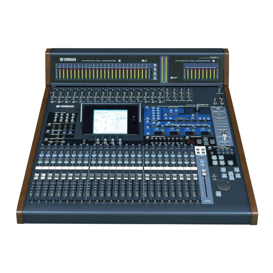
- Page 17 SELECTED CHANNEL Section (p. 21) Display Section (p. 20) AD Input Section (p. 18) Monitor , Phones & T alkback GAIN GAIN GAIN GAIN TALKBACK LEVEL 26dB 26dB 26dB 26dB 26dB 26dB 26dB 26dB 26dB 26dB 26dB 26dB 26dB 26dB 26dB 26dB Section (p.
- Page 18 02R96 AD Input Section q [+48V ON/OFF] switches 26dB (AD 1–16) w [PAD] switches (AD 1–16) e [GAIN] controls GAIN PEAK r [PEAK] indicators SIGNAL t [SIGNAL] indicators y [INSERT ON/OFF] switches INSERT (AD 1–16) GAIN GAIN PEAK SIGNAL 17 18 Channel strips AUTO q Encoders...
- Page 19 02R96 AUX SELECT AUX SELECT q AUX SELECT [DISPLAY] button DISPLAY w [AUX 1]–[AUX 8] buttons ENCODER MODE q ENCODER MODE [DISPLAY] button ENCODER MODE w [PAN] button DISPLAY ASSIGN ASSIGN e [AUX] button r [ASSIGN 1] & [ASSIGN 2] buttons FADER MODE FADER MODE q [FADER] button...
- Page 20 02R96 EFFECTS/PLUG-INS w e r EFFECTS / PLUG INS DISPLAY INTERNAL PLUG INS CHANNEL EFFECTS INSERTS q EFFECTS/PLUG-INS [DISPLAY] button w [INTERNAL EFFECTS] button e [PLUG-INS] button r [CHANNEL INSERTS] button t EFFECTS/PLUG-INS [1]–[4] buttons y Parameter Up/Down buttons u Parameter controls [1]–[4] Display Section q Display w Contrast control...
- Page 21 02R96 SELECTED CHANNEL Section SELECTED CHANNEL ROUTING DISPLAY ACCESS DISPLAY PHASE / DELAY INSERT PAN / SURROUND DISPLAY FOLLOW PAN STEREO DIRECT LINK GRAB EFFECT EVEN DYNAMICS DISPLAY GATE ON COMP ON GATE / COMP GATE THRESHOLD RANGE ATTACK DECAY HOLD COMP THRESHOLD...
- Page 22 02R96 DYNAMICS DYNAMICS DISPLAY GATE ON COMP ON GATE / COMP GATE THRESHOLD RANGE ATTACK DECAY HOLD COMP THRESHOLD RATIO ATTACK RELEASE GAIN q DYNAMICS [DISPLAY] button w [GATE ON] button e [COMP ON] button r [GATE/COMP] button t [THRESHOLD], [RANGE], [ATTACK], [DECAY], [HOLD] ([THRESHOLD], [RATIO], [ATTACK], [RELEASE], [GAIN]) controls y [GATE/COMP] indicators...
- Page 23 02R96 LAYER LAYER q [1–24] & [25–48] buttons w [REMOTE] button 1 24 REMOTE e [MASTER] button 25 48 MASTER STEREO STEREO AUTO q [AUTO] button w [SEL] button e [ON] button r Fader STEREO SCENE MEMORY SCENE MEMORY q SCENE MEMORY [DISPLAY] button w Scene memory display DISPLAY e Edit indicator...
- Page 24 02R96 USER DEFINED KEYS USER DEFINED KEYS DISPLAY q USER DEFINED KEYS [DISPLAY] button w USER DEFINED KEYS [1]–[16] buttons MACHINE CONTROL MACHINE CONTROL LOCATE MEMORY q MACHINE CONTROL DISPLAY [DISPLAY] button w LOCATE MEMORY [1]–[8] buttons e [SET] button r [REW] button t [FF] button y [STOP] button...
- Page 25 02R96 Monitor, Phones & Talkback Section TALKBACK LEVEL q [STUDIO LEVEL] control w [PHONES LEVEL] control PHONES e [PHONES] jack r Talkback mic t [TALKBACK LEVEL] control STUDIO PHONES LEVEL LEVEL MONITOR Section STUDIO MONITOR DISPLAY STUDIO q MONITOR [DISPLAY] button MONITOR DISPLAY w [CONTROL ROOM] button...
- Page 26 Analog Master I/O Section (p. 27) AD Input Section (p. 27) Power Section (p. 28) OMNI OUTs, Digital I/O & Control Section (p. 28) SLOT Section (p. 28)
- Page 27 02R96 AD Input Section q [INPUT A & B (BAL)] connectors w [INSERT I/O +4dB (UNBAL)] connectors (AD 1–16) Analog Master I/O Section q [STUDIO MONITOR OUT +4 dB (BAL)] connectors w [STEREO OUT +4 dB (BAL)] connectors e [2TR IN ANALOG 1 +4 dB (BAL)] connectors r [CONTROL ROOM MONITOR OUT +4 dB (BAL)] connectors t [STEREO OUT –10 dBV (UNBAL)] connectors y [2TR IN ANALOG 2 –10 dBV (UNBAL)] connectors...
- Page 28 02R96 OMNI OUTs, Digital I/O & Control Section q [OMNI OUT +4dB (BAL)] connectors w [SMPTE TIME CODE INPUT] connector e [MTC TIME CODE INPUT] connector r [USB TO HOST] port t [SERIAL TO HOST] port y [2TR OUT DIGITAL COAXIAL 2 & 3] connectors u [2TR OUT DIGITAL AES/EBU 1] connector i [2TR IN DIGITAL COAXIAL 2 &...
- Page 29 02R96 MB02R96 Controls q Channel indicators w [INPUT METERING POSITION] button & indicators e [PEAK HOLD] button r [LAYER] buttons t [OUTPUT METERING POSITION] button & indicators y Meters u [STEREO] meters i [CONTROL ROOM] button o [BUS] meters...
-
Page 30: Circuit Board Layout
02R96 CIRCUIT BOARD LAYOUT 02R96 Bottom AssemblyPower supply unit CPU1 JK2 (2/2) JK2 (2/2) JK2 (1/2) Power supply unit JK2 (1/2) -
Page 31
02R96 Rear Assembly U ANI2 assembly
ANI2 ANI2 assembly 2TRI ANI1 ANI1 ANI1 ANI1 ANI1 ANI1 ANI1 ANI1 ANI1 ANI1 ANI1 ANI1 ANI1 ANI1 ANI1 ANI1 ANI1 ANI1 ANI1 ANI1 ANI1 ANI1 ANI1 ANI1 2TRI ANI2 assembly ANI1 ANI1 ANI1... -
Page 32
02R96 Control Panel Assembly
LCD assembly Insulating sheet LCD assembly Insulating sheet... -
Page 33
02R96 LCD Assembly < > Bottom view < > Bottom view LCDCOM (INV) LCDCOM (CNT) MB02R96
... -
Page 34: Disassembly Procedure
02R96 DISASSEMBLY PROCEDURE Note: Take care not to trap your fingers. After replacing the circuit board or fader of FD1 or FD2, please initialize them. (See page 134.) Disassembling the 02R96 Removing the SP02R96 (Time required: About 5 minutes) 1-1. If the SP02R96 is attached to the 02R96, remove the twelve (12) screws marked [A], and then both sides must be removed. - Page 35 02R96 Rear Assembly U (Time required: About 15 minutes) 4-1. Remove the SP02R96. (See procedure 1.) 4-2. Remove the MB02R96. (See procedure 2.) 4-3. Fasten the control panel assembly. (See procedure 3.) 4-4. Remove the two (2) screws marked [30A] and the five (5) screws marked [30B].
- Page 36 02R96 Bottom Assembly Section CPU1 Circuit Board (Time required: About 15 minutes) 5-1. Remove the SP02R96. (See procedure 1.) 5-2. Remove the MB02R96. (See procedure 2.) 5-3. Fasten the control panel assembly. (See procedure 3.) 5-4. Remove the four (4) screws marked [590]. The CPU1 circuit board can then be removed.
- Page 37 02R96 OPT Circuit Board (Time required: About 20 minutes) 10-1. Remove the SP02R96. (See procedure 1.) 10-2. Remove the MB02R96. (See procedure 2.) 10-3. Fasten the control panel assembly. (See procedure 3.) 10-4. Fasten the rear assembly U. (See procedure 4.) 10-5.
- Page 38 02R96 DC Fan Motor (Time required: About 20 minutes) 15-1. Remove the SP02R96. (See procedure 1.) 15-2. Remove the MB02R96. (See procedure 2.) 15-3. Fasten the control panel assembly. (See procedure 3.) 15-4. Fasten the rear assembly U. (See procedure 4.) 15-5.
-
Page 39
02R96
[590] CPU1 Lithium Battery Battery VN103500 VN103600(Battery holder for VN103500) Notice for back-up battery removal Battery Push the battery as shown in figure, then the battery will pop up. Druk de batterij naar beneden zoals aangeven in de tekening de batterij springt dan naar voren. -
Page 40
02R96
[390] [560] [410A] [330] CPU holder Power supply unit [575] CPU holder [340] [560] [330] [350] Side panel R [460B] JK2 (1/2) [360] Power switch knob [360] [480B] [330]: Bind Head Tapping Screw-B 3.0X8 MFZN2BL (EP600190) [340]: Bind Head Tapping Screw-B A4.0X8 MFZN2BL (VC688800) - Page 41 02R96 Rear Assembly U Section PC Support (Time required: About 15 minutes) 16-1. Remove the SP02R96. (See procedure 1.) 16-2. Remove the MB02R96. (See procedure 2.) 16-3. Fasten the control panel assembly. (See procedure 3.) 16-4. Remove the eleven (11) screws marked [260A], the twenty-four (24) nuts marked [270], the four (4) nuts marked [280] and the twenty-seven (27) knobs marked [300].
- Page 42 02R96 2TRI, ST, STD, PHN Circuit Boards (Time required: About 20 minutes each) 19-1. Remove the SP02R96. (See procedure 1.) 19-2. Remove the MB02R96. (See procedure 2.) 19-3. Fasten the control panel assembly. (See procedure 3.) 19-4. Remove the PC support. (See procedure 16.) 19-5.
-
Page 43
02R96 ANI2 assembly
Locking card spacer [300] x 27 ANI2 assembly x 4 [270] x 24 ANI2 2TRI ANI1 [260A] x 11 x 16 [280] PC support [200A] x 48 [210A] [200B] x 4 [200E] [200D] [200C] [200]: Bonding Tapping Screw-B 3.0X8 MFZN2BL (VN413300) - Page 44 02R96 Control Panel Assembly Section When removing the circuit board, if it is hard to handle while the control panel assembly is fixed slantwise at the front stay, open it widely at 180° for the work. SUB Circuit Board (Time required: About 15 minutes) 22-1.
- Page 45 02R96 PN3+PW Circuit Boards (Time required: About 20 minutes) 26-1. Remove the SP02R96. (See procedure 1.) 26-2. Remove the MB02R96. (See procedure 2.) 26-3. Remove the encoder knob and the hexagonal nut from the control panel side. (Fig.8, Photo.6) 26-4. Fasten the control panel assembly. (See procedure 3.) 26-5.
-
Page 46
02R96 Hexagonal nut Encoder knob Control panel Photo.6 LCD assembly
[260B] x 8 Joy stick knob [410C] [410B] [420] x 5 [440] x 8 [470] [460C] [450A] x 16 [450B] x 8 [400B] x 9 [400A] x 16 Encoder knob [260B]:Flat Head Tapping Screw-B 3.0X8 MFZN2BL (EP600790) -
Page 47
02R96
[180A] x 8 [210B] x 12 Insulating sheet [210C] x 6 Cord holder [180A]: Bind Head Tapping Screw-B 3.0X8 MFZN2BL (EP600190) [210]: Bind Head Tapping Screw-B 3.0X8 MFZN2BL (EP600190) Fig.9 [160B] [165] x 22 [160A] x 20 Cord holder SUB2 holder Insulating sheet... -
Page 48
02R96 [180B]
LCD bracket [120C] Rear LCD case [120C] [120C] [125] [120C]: Bind Head Tapping Screw-B A4.0X8 MFZN2BL (VC688800) [125]: Bind Head Tapping Screw-B A3.0X6 MFZN2BL (VP157900) [180B]: Bind Head Tapping Screw-B A4.0X8 MFZN2BL (VC688800) Fig.11 LCD case assembly ... - Page 49 02R96 LCDCOM (CNT+INV) Circuit Board and LCD (Time required: About 15 minutes each) 30-1. Remove the LCD assembly. (See procedure 29.) 30-2. Remove the four (4) screws marked [180B]. The LCD bracket can then be removed. (Fig.11) 30-3. Remove the six (6) screws marked [120C] and the five (5) screws marked [125].
- Page 50 02R96 DSUB Cable (Time required: About 15 minutes) 34-1. Remove the rear panel. (See procedure 31.) 34-2. Remove the screw marked [130]. The cable holder can then be removed. (Fig.14) 34-3. Remove the DSUB cable with the bushing. (Fig.14) The bushing is not part of the DSUB cable. When you replace the DSUB cable, you should remove the bushing from the cable, and attach in the new cable.
-
Page 51
02R96 DSUB cable Cable holder [80B] Rear panel
Bushing [130] Front panel [50A] [50B] [50]: Bind Head Tapping Screw-B 3.0X8 MFZN2BL (EP600190) [80B]: Bind Head Tapping Screw-B 3.0X8 MFZN2BL (EP600190) [130]: Bind Head Tapping Screw-B 3.0X8 MFZN2BL (EP600190) Fig.14... -
Page 52: Installing I/O Cards
02R96 INSTALLING I/O CARDS This section explains how to install I/O Cards. 1 Turn off the 02R96. 2 Undo the two fixing screws and remove the slot cover, as shown below. Keep the cover and fixing screws in a safe place for future use. 3 Insert the card between the guide rails and slide it all the way into the slot, as shown below. -
Page 53: Lsi Pin Description
02R96 LSI PIN DESCRIPTION M37640M8-138FP (X0157100) CPU ..................... 53 SH7709A FP-208C (XY065A00) CPU ................... 54 HD64F7044F28 (X3086A00) CPU ....................55 HD64F7044F28 (X3197A00) CPU ....................55 YSS910-S (XV988A00) DSP6 (Digital Signal Processor) ............56 YSS919-H (XZ693A00) DSP7 (Digital Signal Processor) ............57 SGH603064F-62F (XV973A00) Gate Array .................. - Page 54 02R96 SH7709A FP-208C (XY065A00) CPU CPU1: IC101 NAME FUNCTION NAME FUNCTION Clock mode CKE/PTK[5] CK enable/Port K Clock mode RAS3L/PTJ[0] DRAM row address strobe/Port J Vcc-RTC*1 Power supply for RTC (1.8 V) RAS2L/PTJ[1] DRAM row address strobe/Port J XTAL2 Crystal oscillator for RTC CASLL/CASL/PTJ[2] Column address strobe (low)/Port J EXTAL2...
- Page 55 02R96 HD64F7044F28 (X3086A00) CPU 02R96/SUB: IC600, 605 HD64F7044F28 (X3197A00) CPU MB02R96/PN2: IC508 NAME FUNCTION NAME FUNCTION PE14 Port E PE15 Port E Data bus Ground Ground Data bus Power supply Address bus Data bus Ground XTAL Crystal oscillator Mode control EXTAL Crystal oscillator Mode control...
- Page 56 02R96 YSS910-S (XV988A00) DSP6 (Digital Signal Processor) DSP: ICA01-04 NAME FUNCTION NAME FUNCTION Power supply (3.3V) Ground Ground DB13 System master clock input (60MHz or 30MHz) DB14 System master clock output (High or 30MHz) DB15 Power supply (5V) DB16 /SYNCI Sync.
- Page 57 02R96 YSS919-H (XZ693A00) DSP7 (Digital Signal Processor) DSP: ICB01-09 NAME FUNCTION NAME FUNCTION PLLEN PLL enable input (0: PLL unuse, 1: PLL use) SIO32 /TEST Test mode setting (0: TEST, 1: Normal) SIO33 AVss Analog ground SIO34 PLL filter SIO35 Serial data bus AVdd Power supply (2.5 V)
- Page 58 02R96 SGH603064F-62F (XV973A00) Gate Array SUB: IC901-903 NAME FUNCTION NAME FUNCTION Data bus Encoder input Ground Data bus Ground Ground Encoder input Data bus Ground Ground Data bus Ground Encoder input Not used Ground RA10 Encoder input RB10 RA11 RB11 Encoder input Address bus RA12...
- Page 59 02R96 YM6604C-S (XU240A00) ACIA (Asynchronous Communication Interface Adapter) DSP: IC703 NAME FUNCTION NAME FUNCTION RESETN Reset Not used Not used IRQ3N Interrupt request Chip select IRQ4N Address strobe Not used LDSN Data strobe IRQ5N Address bus IRQ6N Interrupt request Not used IRQ7N TXD1P Transmit data (1ch)
- Page 60 02R96 MBCG61594-128 (X2162A00) ATSC2 DSP: IC601-604, 651-654 NAME FUNCTION NAME FUNCTION Power supply +3.3V Power supply +3.3V XTST LSI test pin PB_H_M4_SEL Port B audio data input buffer active select Ground PB_O_MUTE Port B mute WT_X CPU interface write input Ground RD_X CPU interface read input...
- Page 61 02R96 ICS2008BV-T (X2832B00) T.C. Reader/Generator JK1: IC305 NAME FUNCTION NAME FUNCTION INTR Interrupt request Clear to send RESET Master reset UART transmit data FRAME Color frame A / B input Ready to send CLICK LTC SYNC input LRCLK SMPTE LTC receive clock LTCIN- SMPTE LTC input - VITCGATE...
- Page 62 02R96 XCS40-3PQ240C (XZ334A00) FPGA (Field Programmable Gate Arrays) DSP: IC056 NAME FUNCTION NAME FUNCTION Ground Power supply +5V CPUCLK Primary global /PROGRAM Active low input /CSIN2 /CSATSC[3] Unrestricted user-programmable Input/Output pin /CSIN3 Unrestricted user-programmable Input/Output pin I/O/PGCK3 Primary global /CSATSC[4] I/O/TDI Test data in (JTAG port) /CSATSC[5]...
- Page 63 02R96 S1D13305F00B100 (XQ595A00) LCDC (LCD Controller) CPU1: IC129 NAME FUNCTION NAME FUNCTION Data bus output for 4 bit dot VRAM address bus XECL S driver enable, chain clock XSCL Data bus shift clock Ground /VWR VRAM read/write X driver latch pulse /VCE Memory control Frame signal for X/Y driver...
-
Page 64: Ic Block Diagram
02R96 IC BLOCK DIAGRAM 02R96 TC74VHC00F (XT229A00) TC74VHC11F (EL) (XT812A00) TC74VHC04F (EL) (XM332A00) CPU1: IC133 DSP: IC411-413 CPU1: IC132 DSP: IC058 ,704 DSP: IC702 Triple 3 Input AND JK1: IC407, 408 MM74HC00SJX (XW105A00) HD74LV04AFPEL (IS000400) FD1: IC138 FD2: IC127 SUB: IC907 HD74LV00AFPEL (IS000000) HD74LVU04AFPEL (XY102A00) SUB: IC704... - Page 65 02R96 TC74VHC139F (EL) (XW324A00) TC74VHC157F (EL) (XT475A00) HD74LV165AFPEL (IS016500) DSP: IC608-611, 655-658 CPU1: IC125 PN1: IC104, 105 JK1: IC401 PN2: IC102, 103, 503 Quad 2 to 1 Multiplexer Dual 2 to 4 Demultiplexer 8-Bit Shift Register SHIFT/ SELECT LOAD CLOCK STROBE CLOCK INHIBIT...
- Page 66 02R96 74VHC541SJX (XY961A00) HD74LV595AFPEL (IS059500) HD74LV245AFPEL (IS024500) DSP: IC070, 071, 106, 803, 806, 852, 903, PN1: IC102, 103 SUB: IC601, 602 908, 909, 951, 952 PN2: IC104-107, 501, 502 TC74HC245AF (XS720A00) 8-Bit Shift Register with Output HD74LV541AFPEL (IS054100) AD1: IC001, 002 Latches DSP: IC001 ADA: IC001, 002, 004, 005...
- Page 67 02R96 SN75121NSR (XU816A00) SN75124NSR (XV930A00) SN75C1168NSR (XU073A00) JK1: IC104 JK1: IC002 JK2 (1/2): IC803 Dual Line Driver Triple Line Receiver Line Driver/Receiver AM26LS31CNSR (XU996A00) UPC319G2 (IG156700) DS26C32ATMX (XU815A00) JK2 (1/2): IC501, 601-604 JK1: IC304 JK1: IC203 JK2 (1/2): IC502-505, 605 Quad Line Driver Voltage Comparator Quad Differential Line Receiver...
- Page 68 02R96 TC7S04F (XM182A00) TC7SH04FU (XS775A00) TC7SH08FU (XR680A00) AD1: IC003 CPU1: IC122 CPU1: IC123, 137 ADA: IC003 DSP: IC012, 066 2 Input AND Gate DA: IC900 Inverter Gate Inverter Gate IN B IN A IN A OUT Y OUT Y TC7SH32FU (TE85L) (XW633A00) TA7291F (XW618A00) DSP: IC051 FD1: IC114-129...
- Page 69 02R96 NJM2068L-D (XM356A00) NJM2904V (TE1) (XR532A00) NJM2068V (TE1) (XT618A00) 2TRI: IC101, 102 CPU1: IC139 FD1: IC133-136 PHN: IC202 FD1: IC112, 113, 137 FD2: IC122-125 ANI1: IC100, 101 FD2: IC109, 110, 126 NJM4560M (T1) (XA862B00) ANI2: IC100, 101, 200, 201 SUB: IC608 Dual Operational Amplifier JK1: IC302 NJM4556AL (XP844A00)
- Page 70 02R96 TC74HC238AF (XT163A00) PN2: IC511 3 to 8 Line Decoder Select Inputs Enable Data Inputs Output SN74HC245NSR (XD838A00) SN75C1168N (XU463A00) TD62M8600F (XV014A00) PN2: IC510 DC1: IC303 PN1: IC101, 300 PN2: IC600 Line Driver/Receiver TC74HC245AF (XS720A00) Source Driver PN1: IC100 Octal 3-State Bus Transceiver OUT1 OUT8 OUT7...
-
Page 71: Circuit Boards
02R96 CIRCUIT BOARDS 02R96 2TRCOM (2TRI) Circuit Board (X2067B0) ........72 2TRCOM (PHN) Circuit Board (X2067B0) ........73 2TRCOM (ST) Circuit Board (X2067B0) ........74 AD1 Circuit Board (XZ020B0) ........... 76/78 ADA Circuit Board (X2064B0) ..........80/82 ANI1 Circuit Board (X2065B0) ............84 ANI2 (ANI2) Circuit Board (X2066B0) ........... -
Page 72: 2Trcom (2Tri) Circuit Board (X2067B0)
02R96 2TRCOM (2TRI) Circuit Board 2TR IN ANALOG 1 2TR IN ANALOG 2 to ADA-CN701 Component side Pattern side 3NA-V863060-2... -
Page 73: 2Trcom (Phn) Circuit Board (X2067B0)
02R96 2TRCOM (PHN) Circuit Board PHONES LEVEL TALKBACK LEVEL PHONES OUT CN202: to TALKBACK MIC to ADA-CN451 Component side Pattern side 3NA-V863060-2... -
Page 74: 2Trcom (St) Circuit Board (X2067B0)
02R96 2TRCOM (ST) Circuit Board STEREO OUT to ADA-CN151 Component side Pattern side 3NA-V863060-2... -
Page 75: Lcdcom (Cnt) Circuit Board (X2160B0)
02R96 LCDCOM (INV) Circuit Board to LCD backlight to BRG-CN018 to CPU1-CN106 to LCD Component side LCDCOM (CNT) Circuit Board CONTRAST Component side 3NA-V824910-2... -
Page 76: Ad1 Circuit Board (Xz020B0)
02R96 AD1 Circuit Board to DSP-CN952 to DSP-CN951 3NA-V863020-2... - Page 77 02R96 CN101: to ANI1#1-CN100 CN102: to ANI1#2-CN100 CN201: to ANI1#3-CN100 CN202: to ANI1#4-CN100 CN301: to ANI1#5-CN100 CN302: to ANI1#6-CN100 CN401: to ANI1#7-CN100 CN402: to ANI1#8-CN100 CN501: to ANI1#9-CN100 CN502: to ANI1#10-CN100 CN601: to ANI1#11-CN100 CN602: to ANI1#12-CN100 to BRG-CN007 Component side 3NA-V863020-2...
- Page 78 02R96 AD1 Circuit Board 3NA-V863020-2...
- Page 79 02R96 Pattern side 3NA-V863020-2...
-
Page 80: Ada Circuit Board (X2064B0)
02R96 ADA Circuit Board to ANI1 #14-CN100 to ANI1 #16-CN100 to ANI2 #2-CN100 to ANI1 #13-CN100 to ANI1 #15-CN100 to ANI2 #1-CN100 to DSP-CN954 to DSP-CN953 3NA-V863030-2... - Page 81 02R96 to ANI2 #4-CN100 to ST-CN301 to PHN-CN201 to ANI2 #3-CN100 to 2TRI-CN101 to STD-CN001 CN351: to PN2 -CN701 to BRG-CN008 to DSP-CN956 to BRG-CN010 Component side 3NA-V863030-2...
- Page 82 02R96 ADA Circuit Board 3NA-V863030-3...
- Page 83 02R96 Pattern side 3NA-V863030-3...
-
Page 84: Ani1 Circuit Board (X2065B0)
02R96 ANI1 Circuit Board GAIN INSERT ON/OFF 26dB +48V SIGNAL PEAK ON/OFF INPUT INSERT I/O to AD1-CN101, CN102, CN201, CN202, CN301, CN302, CN401, CN402, CN501, CN502, CN601, CN602 Component side ADA-CN101, CN102, CN201, CN202 Pattern side 3NA-V863040-2... -
Page 85: Ani2 (Ani2) Circuit Board (X2066B0)
02R96 ANI2 (LED) Circuit Board ANI2 (ANI2) Circuit Board SIGNAL GAIN GAIN PEAK SIGNAL PEAK INPUT to ADA-CN301, CN401, CN501, CN601 Component side Pattern side 3NA-V863050-2... -
Page 86: Brg Circuit Board (X2062B0)
02R96 BRG Circuit Board to Power Supply Unit-CN105 to Power Supply Unit to Power Supply Unit -CN103 to FAN not installed -CN102 to JK2 (1/2) -CN902 to JK1 -CN453 to DSP -CN963 to DSP-CN961 CN007: to AD1-CN001 CN008: to ADA-CN001 CN009: to DA-CN001 CN010: to ADA-CN005 3NA-V922160-2... - Page 87 02R96 CN021: ply Unit to Power Supply Unit to Power Supply Unit CN020: -CN104 -CN101 installed to PN2-CN500 to PN1 -CN101 to FD2 -CN102 to FD1 -CN102 to SUB -CN702 CN001 not installed to DSP-CN962 -CN001 to LCDCOM(INV)-CN901 CN001 -CN005 Component side 3NA-V922160-2...
- Page 88 02R96 BRG Circuit Board 3NA-V922160-2...
- Page 89 02R96 Pattern side 3NA-V922160-2...
-
Page 90: Cpu1 Circuit Board (X0383C0)
02R96 CPU1 Circuit Board to SUB-CN701 not used not used to LCDCOM (INV)-CN903 not used (for check) not installed not installed not used (for check) to DSP-CN105 to DSP-CN104 Component side Lithium Battery Battery VN103500 VN103600(Battery holder for VN103500) Notice for back-up battery removal Battery Push the battery as shown in figure, then the battery will pop up. - Page 91 02R96 CPU1 Circuit Board Pattern side 3NA-V846880-3...
-
Page 92: Circuit Board (Xz021C0)
02R96 DA Circuit Board to BRG -CN009 OMNI OUT to DSP -CN955 Component side 3NA-V910670-2... - Page 93 02R96 DA Circuit Board Pattern side 3NA-V910670-2...
- Page 94 02R96 DSP Circuit Board CN805: to OPT-CN807 CN90 to BRG-CN012 to BRG-CN016 to ADA-CN004 to JK1-CN452 to J CN953: to ADA -CN003 to OPT-CN802 CN804: to OPT -CN804 CN954: to ADA -CN002 CN955: to DA -CN901 CN951: to AD1 -CN003 to OPT-CN801 to OPT-CN803 to AD1-CN002...
- Page 95 02R96 CN904: to JK2 (1/2)-CN903 to JK2 (1/2)-CN904 to JK1-CN451 to JK2 (1/2)-CN901 to BRG-CN013 to CPU1-CN104 to CPU1-CN105 Component side 3NA-V846890-2...
- Page 96 02R96 DSP Circuit Board 3NA-V846890-2...
- Page 97 02R96 Component side 3NA-V846890-2 2 layer...
- Page 98 02R96 DSP Circuit Board 3NA-V846890-2...
- Page 99 02R96 Component side 3NA-V846890-2 5 layer...
- Page 100 02R96 DSP Circuit Board 3NA-V846890-3...
- Page 101 02R96 Pattern side 3NA-V846890-3...
-
Page 102: Fd1 Circuit Board (X2053B0)
02R96 FD1 Circuit Board to SUB-CN901 to SUB-CN900 FADER 3NA-V862690-2... - Page 103 02R96 to BRG-CN022 Component side 3NA-V862690-2...
- Page 104 02R96 FD1 Circuit Board 3NA-V862690-3...
- Page 105 02R96 Pattern side 3NA-V862690-3...
-
Page 106: Fd2 Circuit Board (X2054B0)
02R96 FD2 Circuit Board to SUB-CN902 to BRG-CN023 STEREO FADER Component side 3NA-V862700-2... - Page 107 02R96 FD2 Circuit Board Pattern side 3NA-V862700-3...
-
Page 108: Jkcom (Jk1) Circuit Board (X2058B0)
WORD CLOCK 2TR IN DIGITAL 2TR OUT DIGITAL TO HOST TIME CODE INPUT COAXIAL COAXIAL 75Ω ON/OFF AES/EBU AES/EBU SMPTE SERIAL to DSP-CN902 to DSP-CN901 to BRG-CN014... -
Page 110: Jkcom (Jk2 (1/2)) Circuit Board (X2058B0)
02R96 JKCOM (JK2 (1/2)) Circuit Board to BRG-CN015 to DSP-CN903 to DSP-CN905 THRU CASCADE OUT METER MIDI (from MB02R96) 3NA-V846900-2 3NA-V846900-3... -
Page 111: Jkcom (Jk2 (2/2)) Circuit Board (X2058B0)
02R96 JKCOM (JK2 (2/2)) Circuit Board CN804: to JK2 (2/2)-CN802 to DSP-CN904 CN805: to JK2 (2/2)-CN803 to JK2 (1/2)-CN805 to JK2 (1/2)-CN804 CASCADE IN CONTROL Component side Component side Pattern side Pattern side 3NA-V846900-2 3NA-V846900-3... -
Page 112: Opt Circuit Board (X2060B0)
to DSP-CN804 SLOT4 SLOT3 to DSP-CN803 to DSP -CN805 to DSP-CN802 to DSP-CN801 SLOT2 SLOT1... -
Page 114: Pn1Com (Pn1) Circuit Board (X2050B0)
02R96 PN1COM (PN1) Circuit Board to SUB -CN906 to SUB -CN905 to SUB -CN903 to SUB -CN904 3NA-V924550-2... - Page 115 02R96 to BRG -CN019 Component side 3NA-V924550-2...
- Page 116 02R96 PN1COM (PN1) Circuit Board 3NA-V924550-2...
- Page 117 02R96 Pattern side 3NA-V924550-2...
-
Page 118: Pn1Com (Pn3) Circuit Board (X2050B0)
02R96 PN1COM (PN3) Circuit Board to PN2-CN501 Component side PN1COM (PW) Circuit Board 3NA-V924550-2 Component side... - Page 119 02R96 PN1COM (PN3) Circuit Board Pattern side PN1COM (PW) Circuit Board Pattern side 3NA-V924550-2...
-
Page 120: Pn1Com (Sub) Circuit Board (X2050B0)
02R96 PN1COM (SUB) Circuit Board to FD1-CN103 to FD1-CN101 to CPU1 -CN101 not used (for check) not used (for debug SUB1) to PN1 -CN102 to PN1-CN100 to PN1-CN401 to PN1-CN400 3NA-V924550-2... - Page 121 02R96 to FD2-CN101 to BRG-CN024 to PN2 -CN100 CN908: to PN2 -CN702 to PN2 -CN401 Component side 3NA-V924550-2...
- Page 122 02R96 PN1COM (SUB) Circuit Board 3NA-V924550-2...
- Page 123 02R96 Pattern side 3NA-V924550-2...
-
Page 124: Pn2Com (Pn2) Circuit Board (X2051B0)
02R96 PN2COM (PN2) Circuit Board to SUB-CN908 to BRG PN2COM (JS) Circuit Board JOY STICK Component side 3NA-V862670-2... - Page 125 02R96 CN701: to ADA-CN351 to BRG-CN020 to SUB-CN909 to SUB-CN907 VR700:SURROUND MONITOR LEVEL to PN3 VR701:CONTROL ROOM LEVEL -CN500 Component side 3NA-V862670-2...
- Page 126 02R96 PN2COM (PN2) Circuit Board 3NA-V862670-2...
- Page 127 02R96 PN2COM (JS) Circuit Board Pattern side Pattern side 3NA-V862670-2...
-
Page 128: Std Circuit Board (X2068B0)
02R96 STD Circuit Board STUDIO LEVEL STUDIO MONITOR OUT CONTROL ROOM MONITOR OUT to ADA-CN251 Component side Pattern side 3NA-V863070-2 3NA-V863070-3... -
Page 129: Dc1 Circuit Board (Xz038B0)
02R96 DC1 Circuit Board to PN1-CN102 installed to PN2-CN500 not installed to METER (02R96) Component side 3NA-V863080-2... -
Page 130: Pncom (Pn1) Circuit Board (X2069C0)
02R96 PNCOM (PN1) Circuit Board to DC1-CN302 to PN2-CN501 3NA-V862150-2 3NA-V862150-2a... - Page 131 02R96 to DC1-CN302 to PN2-CN501 to PN2-CN502 Component side Pattern side 3NA-V862150-2 3NA-V862150-2a...
-
Page 132: Pncom (Pn2) Circuit Board (X2069C0)
not used to DC1-CN303 (for DSP check) to PN1-CN101 to PN1-CN100... -
Page 134: Inspections
02R96 INSPECTIONS Perform the Check of 02R96. 1. Preparation The LCD screen will change as shown below, and the selected DSP7 program will start up. 1-1. Condition Conditioned as follows unless specified: Supplementary information) ****H**M [Elapsed Time] and [ ] will not be WORD CLOCK to be INT 96kHz. - Page 135 02R96 w Special learning d. Start up the application to be used for writing data into the computer. a. Set the layer to “MASTER”, operate the CH9 e. Select the I/O port. fader to divide all 100mm strokes into equal f.
- Page 136 02R96 2. Check of ANALOGUE IN/OUT at WORD 2-2. STEREO OUT L/R (PIN) CLOCK INT 96 kHz Condition: Input from the CH1 (XLR). 2-1. STEREO OUT L/R (XLR) Condition: Input from the CH1 (XLR). Gain (L/R common) Input Frequency Input Level Specified output level Permissible range Gain (L/R common) 1kHz...
- Page 137 02R96 Level gap between L/R Level gap between L/R Level gap measured in q to be decided as follows: Level gap measured in q to be decided as follows: Permissible range Permissible range Within 1dB Within 1dB Cross talk between L and R Cross talk between L and R Condition: PAN to fully lean to the L side.
- Page 138 02R96 Residual noise (OMNI OUT 1~8) Level gap between L/R Level gap measured in q to be decided as follows: Condition: [BUS OUT] key to be switched OFF. Permissible range Permissible range Within 1dB -92dBu or below Level gap among the terminals [OMNI OUT 1~8] Maximum output (L/R common) Level gap measured in q and w to be decided as Condition: To output –6dB from the built-in...
- Page 139 02R96 2-8. 2TR IN ANALOG 2 L/R Noise level (CH1~16) Condition: Check at the [STEREO OUT L] terminal (XLR). Condition: Measured CH IN to be shorted at 150Ω. Permissible range Gain (L/R common) -64dBu or below Input Frequency Input Level Specified output level Permissible range However, if not be within the above range EIN, 1kHz...
- Page 140 02R96 2-10. CH IN 17~24 (PHONE) Light ON Condition: Check at the [STEREO OUT L] terminal (XLR). Reference output level LED level Input frequency Input level (INSERT OUT) GAIN MAX PEAK 1kHz +23dBu +17dBu Gain (CH17~24) SIGNAL 1kHz -8dBu -14dBu Input Frequency Input Level Specified output level Permissible range...
- Page 141 02R96 3-3. STUDIO MONITOR OUT L/R Residual noise (L/R common) Condition: Input from the CH1 (XLR). Condition: [2TR IN ANALOG 1] terminal to be Set the [STUDIO LEVEL] control to MAX. shorted at 150Ω. Turn ON the [STEREO] key of STUDIO. Permissible range -87dBu or below Distortion factor (L/R common)
- Page 142 02R96 f Characteristic (2TR DIGITAL OUT 1) Set the frequency setting of System Condition: Permissible range of 1kHz to be standard. Two (Sample Rate) to 44.1kHz. Input Frequency Input Level Permissible range Turn ON SRC of CH to be measured. 20Hz +10dBu -1.0~0.5dB...
- Page 143 02R96 2TR DIGITAL IN 1,2,3 5. Measuring jitter Condition: Set WORD CLOCK INT to 96kHz. Condition: Use System Two. Check at the [STEREO OUT L/R] Select Sec, PK terminal (XLR). BW: Select 700Hz~100kHz. Set the frequency setting of System Check at the [2TR DIGITAL OUT1] Two (Sample Rate) to 44.1kHz.
- Page 144 02R96...
- Page 145 02R96...
- Page 146 02R96...
- Page 147 02R96...
- Page 148 02R96...
- Page 149 02R96...
- Page 150 02R96...
- Page 151 02R96...
- Page 152 02R96...
- Page 153 02R96...
-
Page 154: Service Check Program
Example of screen for the entire check items using the [ENTER] key. 2) Choice of OK or NG displays the next check item --- 02R96 test --- (C)YAMAHA 2002 automatically. 3) Pressing the [DBC] key while the entry of OK/NG decision F/W Ver. MAIN Vx.xx METER Vx.xx... - Page 155 02R96 1. Service Check 1-1 MCS(FPGA) Test Contents: Read/Write the Reg. (00, 0f, 10, 11, 15, 16) Common contents of FPGA to compare and judge and then 1) The contents and example screens of execution for readout the Reg.12 (Ver) and display it. each check item are displayed.
- Page 156 02R96 Test item for DSP6 Test item for DSP7 1-14 WORD CLOCK Test 1: CPU Interface (Data bus) 1: CPU Interface (Data Bus) Contents: Count FPGA over WORD CLOCK OUT→IN 2: CPU Interface (Data bus) 2: CPU Interface (Chip Select) for automatic judge (Fs=44.1/48/88.2/96kHz).
- Page 157 02R96 1-18 TIME Code Test For the lighting order, see 2. Supplement “LED lighting order Contents: Receiving the MIDI OUT signal from the unit Fig. 1,2.” For 7-SegLEDs, they light in the order 1..9,0-dot. and compare with the Send/Receive signal 1-27 PANEL ALL LED Test “Test MTC¥n”...
- Page 158 02R96 1) Specified position of FADER Position Example of execution screen CH1-24 STEREO --- FADER Tsense --- FADER Position 1 0dB at the index of the Fade’s left -10dB FADER Position 2 -10dB at the index of the Fade’s left -20dB OK CH11 ** NG CH13...
- Page 159 02R96 1-32 ENCODER (etc.) Test 1-37 METER SW Test Contents: From CH1, check the rotation response of Contents: Press the SWs of MB02R96 to check if the Encoder of other than CH24. corresponding LED turns ON/OFF. The way of operation is the same as 1-31. Example of execution screen Example of execution screen --- METER SW ---...
- Page 160 02R96 2. Supplement LCD Display Fig.1 PANEL SW operation sequence Screen (For operation sequence, see “SW operation Fig.1and 2.) LCD display: 53 columns x 30 lines (320 x 240 dots with Font5x7) Pressed SW will disappear. The next SW to be pressed will blink.
- Page 161 02R96 SW Operation Fig.1 GROUP1 SW Operation Fig.2 GROUP3 GROUP2...
- Page 162 02R96 LED Lighting Sequence Fig.1...
- Page 163 02R96 LED Lighting Sequence Fig.2...
- Page 164 02R96...
- Page 165 02R96...
- Page 166 02R96...
- Page 167 02R96...
- Page 168 02R96...
- Page 169 02R96...
- Page 170 02R96...
- Page 171 02R96...
- Page 172 02R96...
- Page 173 02R96...
-
Page 174: Test Program
02R96 TEST PROGRAM Execute the test program for MB02R96. 1. Preparation 1) Connect the D-sub 15pin cable to the [METER] terminal in the rear of 02R96. 2) If 02R96 is not provided, supply +12V between +12V and GND from an external power supply. Note) Loop Back test will result in ERROR if independent test is carried out with being connected to the body of 02R96. - Page 175 02R96...
-
Page 176: Using Bulk Dump
02R96 USING BULK DUMP 02R96 data can be stored to an external MIDI device, such as a MIDI data filer, by using MIDI Bulk Dump. 1 Use the DISPLAY ACCESS [MIDI] button to locate the Bulk Dump page. 2 To transmit data, use the CATEGORY parameters to select the type of data you want to transmit, select the TRANSMIT button, and then press [ENTER]. -
Page 177: Checking The Battery
02R96 CHECKING THE BATTERY The condition of the internal memory-backup battery can be checked as follows. 1 Use the DISPLAY ACCESS [UTILITY] button to locate the Battery Check page. If the Status is “Okay,” the battery is okay. If the Status is “Getting Low,”... -
Page 178: Midi Data Format
02R96 MIDI DATA FORMAT Scene Memory to Program Change Table Program Initial User Program Initial User Program Initial User Change # Scene # Scene # Change # Scene # Scene # Change# Scene # Scene # — — — — —... - Page 179 02R96 Initial Parameter to Control Change Table High High NO ASSIGN FADER L CHANNEL INPUT28 FADER L CHANNEL INPUT29 FADER H CHANNEL INPUT1 FADER L CHANNEL INPUT30 FADER H CHANNEL INPUT2 FADER L CHANNEL INPUT31 FADER H CHANNEL INPUT3 FADER H CHANNEL INPUT4 CHANNEL...
- Page 180 02R96 MIDI Data Format 1. CHANNEL MESSAGE 4.2.2 PARAMETER CHANGE Command rx/tx function Command rx/tx function F0 43 1n 3E 0B PARAMETER rx/tx 02R96-specific parameter 8n NOTE OFF Control the internal effects CHANGE change 9n NOTE ON Control the internal effects F0 43 3n 3E 0B PARAMETER rx/tx 02R96-specific parameter...
- Page 181 02R96 If [TABLE] is selected 8. CONTINUE (FB) Reception Control change STATUS 1011nnnn Bn This message is received if the automix TIME REFERENCE setting is MIDI Control number (0-95, 102-119) DATA 0ccccccc cc CLOCK, and will cause automix to start from the current song position. In Control value (0-127) 0vvvvvvv vv actuality, automix will start when the next TIMING CLOCK is received af-...
- Page 182 Program change table. d[0~6]: actual data System exclusive message STATUS 11110000 F0 b[0~7]: bulk data Manufacture's ID number (YAMAHA) ID No. 01000011 43 b[0] = 0; n=0-15 (Device number=MIDI Channel) SUB STATUS 0000nnnn 0n for( I=0; I<7; I++){ Universal bulk dump FORMAT No.
- Page 183 The second and third bytes of the DATA NAME indicate the bank num- System exclusive message STATUS 11110000 F0 ber. Manufacture's ID number (YAMAHA) ID No. 01000011 43 Be aware that the state of the transmission destination will (in some cases) n=0-15 (Device number=MIDI Channel) SUB STATUS 0010nnnn 2n change if the same bank is being used.
- Page 184 12.2.11 Control change table bulk dump format 0ddddddd de System exclusive message STATUS 11110000 F0 ee=(Invert('L'+...+de)+1)&0x7F CHECK SUM 0eeeeeee ee Manufacture's ID number (YAMAHA) ID No. 01000011 43 End of exclusive 11110111 F7 n=0-15 (Device number=MIDI Channel) SUB STATUS 0000nnnn 0n Universal bulk dump FORMAT No.
- Page 185 00111000 38 For reception by the 02R96, only the user area is valid. (4-127, 256-) 01000011 43 System exclusive message 00110101 35 STATUS 11110000 Manufacture's ID number (YAMAHA) 00110100 34 ID No. 01000011 n=0-15 (Device number=MIDI DATA NAME 01010001 51...
- Page 186 LIB. No. H 0bbbbbbb bh 256-259(Effect1-4 current) System exclusive message STATUS 11110000 F0 LIB. No. L 0bbbbbbb bl Manufacture's ID number (YAMAHA) ID No. 01000011 43 total block number(minimum number BLOCK INFO. 0ttttttt tt n=0-15 (Device number=MIDI Channel) SUB STATUS 0010nnnn 2n...
- Page 187 For reception by the 02R96, only the user area is valid. (1-32, 256) data) System exclusive message STATUS 11110000 F0 0bbbbbbb bl Manufacture's ID number (YAMAHA) ID No. 01000011 43 total block number(minimum number BLOCK INFO. 0ttttttt tt is 0)
- Page 188 0:Library no.0 - 32:Library no.32, 256:current data 00110100 34 System exclusive message STATUS 11110000 F0 DATA NAME 01000001 41 Manufacture's ID number (YAMAHA) ID No. 01000011 43 0-3 (SLOT1-4) 0mmmmmmm mm n=0-15 (Device number=MIDI Channel) SUB STATUS 0010nnnn 2n 0mmmmmmm ml Universal bulk dump FORMAT No.
- Page 189 ADDRESS 00000010 02 System exclusive message STATUS 11110000 F0 Element No. 0eeeeeee ee Manufacture's ID number (YAMAHA) ID No. 01000011 43 (If ‘ee’ is 0, ‘ee’ is expanded to two n=0-15 (Device number=MIDI Channel) SUB STATUS 0011nnnn 3n bytes) MODEL ID (digital mixer)
- Page 190 0-513, 16383 tx/rx STATUS 11110000 F0 System exclusive message EFF LIB STORE 0x24 53-128 0-7, 16383 tx/rx Manufacture's ID number (YAMAHA) ID No. 01000011 43 CHANNEL LIB STORE 0x26 3-128 0-513, 16383 tx/rx n=0-15 (Device number=MIDI Channel) SUB STATUS 0001nnnn 1n...
- Page 191 In the case of PAIR, you must specify channels for which pair- System exclusive message STATUS 11110000 F0 ing is possible. Manufacture's ID number (YAMAHA) ID No. 01000011 43 In the case of PAIR ON with COPY, you must specify Source Channel as the copy source, and Destination Channel as the...
- Page 192 End of exclusive 11110111 F7 System exclusive message STATUS 11110000 F0 12.3.24 Parameter request (Remote Time Counter) Manufacture's ID number (YAMAHA) ID No. 01000011 43 Reception n=0-15 (Device number=MIDI Channel) SUB STATUS 0001nnnn 1n This is received if [Parameter change RX] is ON and the [Rx CH] matches...
-
Page 193: Midi Implementation Chart
02R96 YAMAHA [Digital Mixing Console-Internal Parameters] Date: 20 Mar. 2002 MIDI Implementation Chart Model: 02R96 Version: 1.0 Function... Transmitted Recognized Remarks Basic Default 1–16 1–16 Memorized Channel Changed 1–16 1–16 Default OMNI off/OMNI on Mode Messages Memorized Altered ************** Note 0–127... -
Page 194: Parts List
DIGITAL MIXING CONSOLE PARTS LIST CONTENTS OVERALL ASSEMBLY ..........2 BOTTOM ASSEMBLY ........5 REAR ASSEMBLY U ........10 CONTROL PANEL ASSEMBLY ....13 LCD ASSEMBLY ..........18 ELECTRICAL PARTS ........... 21 Notes : DESTINATION ABBREVIATIONS A : Australian model M : South African model B : British model O : Chinese model... - Page 195 02R96 OVERALL ASSEMBLY Rear view Left side view Rear assembly U: : Right side is the same too.) See page 10. U.S.A. model only Top view Control panel assembly: See page 13. Front view Bottom assembly: See page 5.
- Page 196 Bottom view Top view Control panel assembly: Bottom assembly: Rear assembly U: See page 13. See page 5. See page 10. Right side view...
- Page 197 02R96 PART NO. DESCRIPTION REMARKS REF NO. RANK OVERALL ASSEMBLY 02R96 Overall Assembly (V781630) Overall Assembly (V781640) Overall Assembly H,B,W (V781650) Overall Assembly (V980380) Bottom Assembly (V781680) Rear Assembly U UPPER (V781700) Bind Head Tapping Screw-B A4.0X8 MFZN2BL VC688800 VP156900 Bind Head Screw A4.0X12 MFZN2BL VZ678500...
- Page 198 02R96 BOTTOM ASSEMBLY Top view Rear view Left side view Right side view Bottom view Front view A view...
- Page 199 02R96 Front view B view Top view 840 910 Right side view 850 860 1010 1000 1000 450a Rear view...
- Page 200 Top view Top view 450b Rear view Rear view...
- Page 201 02R96 PART NO. DESCRIPTION REMARKS REF NO. RANK BOTTOM ASSEMBLY 02R96 (V781680) V 8 6 8 1 8 0 0 Bottom Chassis V 8 9 9 1 5 0 0 Foot VR138400 Bind Head Tapping Screw-B 4.0X12 MFZN2BL Caution Label (VV85650) V 8 8 0 6 5 0 0 OPT Angle...
- Page 202 02R96 PART NO. DESCRIPTION REMARKS REF NO. RANK VY689800 Jumper Wire FVP=2.0C26SB6-250 V 9 4 6 8 4 0 0 Jumper Wire FVP=2.0C26SB9-150 VT644300 Jumper Wire FVP=2.0C26SB11-200 V 8 9 4 8 7 0 0 Jumper Wire FVP=2.0C26SB10-200 V 8 9 4 8 6 0 0 Jumper Wire FVP=2.0C26SB9-200 V 8 9 4 8 8 0 0...
- Page 203 Top view...
- Page 204 Top view 140c 140b 140a ANI2 assembly Rear view...
- Page 205 02R96 PART NO. DESCRIPTION REMARKS REF NO. RANK REAR ASSEMBLY U UPPER 02R96 (V781700) V 7 9 8 7 7 0 0 Shield Plate L LEFT V 7 9 8 7 8 0 0 Shield Plate R RIGHT VC688800 Bind Head Tapping Screw-B A4.0X8 MFZN2BL V 8 6 7 8 2 0 0 Rear Panel U...
- Page 206 02R96 CONTROL PANEL ASSEMBLY Bottom view...
- Page 207 02R96 Bottom view 120a...
- Page 208 02R96 Bottom view...
- Page 209 02R96 LCD assembly: See page 18. Top view...
- Page 210 02R96 PART NO. DESCRIPTION REMARKS REF NO. RANK CONTROL PANEL ASSEMBLY 02R96 (V781690) V 8 6 7 7 2 0 0 Control Panel Adhesive Tape (VE36240) V 8 1 2 7 0 0 0 LED Lens PEAK 1-24, SIGNAL 1-24 V 6 4 3 5 0 0 0 Cover, 7 Seg.
- Page 211 Left side view Top view Bottom view Bottom view 190a 190b...
- Page 212 Right side view Bottom view Left side view Bottom view...
- Page 213 02R96 PART NO. DESCRIPTION REMARKS REF NO. RANK V 6 4 2 8 8 0 0 LCD ASSEMBLY 02R96 V 6 4 3 7 4 0 0 LCD Case Assembly LCD Case (V636340) LCD Side Panel L LEFT (V643630) LCD Side Panel R RIGHT (V643650) V 6 3 6 3 5 0 0...
- Page 214 02R96 ELECTRICAL PARTS PART NO. DESCRIPTION REMARKS REF NO. RANK ELECTRICAL PARTS 02R96 V 8 6 3 2 6 0 0 Circuit Board 2TRI (2TRCOM) (V863060)(X2067B0) V 8 6 3 2 4 0 0 Circuit Board PHN (2TRCOM) (V863060)(X2067B0) V 8 6 3 2 5 0 0 Circuit Board ST (2TRCOM) (V863060)(X2067B0)
- Page 215 02R96 PART NO. DESCRIPTION REMARKS REF NO. RANK C219 UR847470 Electrolytic Cap. 47.00 25.0V C220 UR847470 Electrolytic Cap. 47.00 25.0V C221 VT439600 Monolithic Ceramic Cap. 0.100 50V Z -224 VT439600 Monolithic Ceramic Cap. 0.100 50V Z C226 VT439600 Monolithic Ceramic Cap. 0.100 50V Z -228 VT439600...
- Page 216 02R96 PART NO. DESCRIPTION REMARKS REF NO. RANK R119 HB026820 Metal Film Resistor 8.2K 1/4 F R120 HB026820 Metal Film Resistor 8.2K 1/4 F R121 HB027100 Metal Film Resistor 10.0K 1/4 F R122 HB027100 Metal Film Resistor 10.0K 1/4 F R123 HB027120 Metal Film Resistor...
- Page 217 02R96 PART NO. DESCRIPTION REMARKS REF NO. RANK R415 HF457100 Carbon Resistor 10.0K 1/4 J R416 HF457100 Carbon Resistor 10.0K 1/4 J R417 HF454100 Carbon Resistor 10.0 1/4 J R418 HB026150 Metal Film Resistor 1.5K 1/4 F R419 HB026120 Metal Film Resistor 1.2K 1/4 F R420 HF457100...
- Page 218 02R96 PART NO. DESCRIPTION REMARKS REF NO. RANK C303 US062220 Ceramic Capacitor-SL(chip) 220P 50V J -306 US062220 Ceramic Capacitor-SL(chip) 220P 50V J C307 UA353220 Mylar Capacitor 2200P 50V J C308 UA353220 Mylar Capacitor 2200P 50V J C309 UU147220 Electrolytic Cap. 22.00 25.0V C310 US145100...
- Page 219 02R96 PART NO. DESCRIPTION REMARKS REF NO. RANK C615 UU167100 Electrolytic Cap. 10.00 50.0V C616 US135220 Ceramic Capacitor-F (chip) 0.2200 16V Z C617 US135220 Ceramic Capacitor-F (chip) 0.2200 16V Z C618 US145100 Ceramic Capacitor-F (chip) 0.1000 25V Z C619 UU167100 Electrolytic Cap.
- Page 220 02R96 PART NO. DESCRIPTION REMARKS REF NO. RANK R209 HB026180 Metal Film Resistor 1.8K 1/4 F R210 HB026180 Metal Film Resistor 1.8K 1/4 F R211 HB026220 Metal Film Resistor 2.2K 1/4 F -214 HB026220 Metal Film Resistor 2.2K 1/4 F R215 HB026270 Metal Film Resistor...
- Page 221 02R96 PART NO. DESCRIPTION REMARKS REF NO. RANK R611 HB026220 Metal Film Resistor 2.2K 1/4 F -614 HB026220 Metal Film Resistor 2.2K 1/4 F R615 HB026270 Metal Film Resistor 2.7K 1/4 F R616 HB027110 Metal Film Resistor 11.0K 1/4 F R617 HB026270 Metal Film Resistor...
- Page 222 02R96 PART NO. DESCRIPTION REMARKS REF NO. RANK C209 UU147220 Electrolytic Cap. 22.00 25.0V C210 UB045100 Monolithic Ceramic Cap. F 0.100 50V Z C211 UU147220 Electrolytic Cap. 22.00 25.0V C212 UB045100 Monolithic Ceramic Cap. F 0.100 50V Z C213 UB045100 Monolithic Ceramic Cap.
- Page 223 02R96 PART NO. DESCRIPTION REMARKS REF NO. RANK C401 UU147470 Electrolytic Cap. 47.00 25.0V C402 UU147470 Electrolytic Cap. 47.00 25.0V C403 UB052220 Monolithic Ceramic Cap. SL 220P 50V J -406 UB052220 Monolithic Ceramic Cap. SL 220P 50V J C407 UA353220 Mylar Capacitor 2200P 50V J C408...
- Page 224 02R96 PART NO. DESCRIPTION REMARKS REF NO. RANK C569 UB044100 Monolithic Ceramic Cap. F 0.010 50V Z C570 UB044100 Monolithic Ceramic Cap. F 0.010 50V Z C601 UU147470 Electrolytic Cap. 47.00 25.0V C602 UU147470 Electrolytic Cap. 47.00 25.0V C603 UB052220 Monolithic Ceramic Cap.
- Page 225 02R96 PART NO. DESCRIPTION REMARKS REF NO. RANK CN202 V I 3 7 8 7 0 0 Connector Socket MQ 9P SE CN251 V I 3 7 9 2 0 0 Connector Socket MQ 12P SE CN301 V I 3 7 8 7 0 0 Connector Socket MQ 9P SE CN351...
- Page 226 02R96 PART NO. DESCRIPTION REMARKS REF NO. RANK R017 HF456220 Carbon Resistor 2.2K 1/4 J R018 RD258100 Carbon Resistor (chip) 100.0K 0.1 J R019 RD257100 Carbon Resistor (chip) 10.0K 0.1 J R020 HF457100 Carbon Resistor 10.0K 1/4 J R021 RD258100 Carbon Resistor (chip) 100.0K 0.1 J R022...
- Page 227 02R96 PART NO. DESCRIPTION REMARKS REF NO. RANK R309 HB026180 Metal Film Resistor 1.8K 1/4 F R310 HB026180 Metal Film Resistor 1.8K 1/4 F R311 HB026220 Metal Film Resistor 2.2K 1/4 F -314 HB026220 Metal Film Resistor 2.2K 1/4 F R315 HB026270 Metal Film Resistor...
- Page 228 02R96 PART NO. DESCRIPTION REMARKS REF NO. RANK R511 HB026220 Metal Film Resistor 2.2K 1/4 F -514 HB026220 Metal Film Resistor 2.2K 1/4 F R515 HB026270 Metal Film Resistor 2.7K 1/4 F R516 HB027110 Metal Film Resistor 11.0K 1/4 F R517 HB026270 Metal Film Resistor...
- Page 229 02R96 PART NO. DESCRIPTION REMARKS REF NO. RANK R829 RD250000 Carbon Resistor (chip) 0.0 0.0 J TR001 V J 9 2 7 1 0 0 Transistor 2SC2712 Y TR002 V J 9 2 7 1 0 0 Transistor 2SC2712 Y TR003 VQ395600 Transistor...
- Page 230 02R96 PART NO. DESCRIPTION REMARKS REF NO. RANK R116 VP434800 Metal Film Resistor 18.0 1/4 F R117 VP442700 Metal Film Resistor 36.0K 1/4 F R118 VP440900 Metal Film Resistor 6.2K 1/4 F R119 VP440900 Metal Film Resistor 6.2K 1/4 F R120 VP442700 Metal Film Resistor...
- Page 231 02R96 PART NO. DESCRIPTION REMARKS REF NO. RANK C124 VF466600 Ceramic Capacitor-SL 10P 50V J C125 UU148100 Electrolytic Cap. 100.00 25.0V C126 UU148100 Electrolytic Cap. 100.00 25.0V C201 V J 0 9 7 4 0 0 Electrolytic Cap.-KL 10.00 50.0V C202 V J 0 9 7 4 0 0 Electrolytic Cap.-KL...
- Page 232 02R96 PART NO. DESCRIPTION REMARKS REF NO. RANK R131 HB027100 Metal Film Resistor 10.0K 1/4 F R132 HB028100 Metal Film Resistor 100.0K 1/4 F R133 HB028100 Metal Film Resistor 100.0K 1/4 F R134 HF458100 Carbon Resistor 100.0K 1/4 J R135 HF458100 Carbon Resistor 100.0K 1/4 J...
- Page 233 02R96 PART NO. DESCRIPTION REMARKS REF NO. RANK C040 UR639220 Electrolytic Cap. 2200 16.0V C051 US145100 Ceramic Capacitor-F (chip) 0.1000 25V Z C052 V 8 8 7 8 5 0 0 Electrolytic Cap. (chip) C054 V 8 8 7 8 9 0 0 Electrolytic Cap.
- Page 234 02R96 PART NO. DESCRIPTION REMARKS REF NO. RANK L001 V 9 2 2 4 3 0 0 Coil CDRH127-470MC 47uH L002 V 9 2 2 4 3 0 0 Coil CDRH127-470MC 47uH R004 RD257100 Carbon Resistor (chip) 10.0K 0.1 J R005 RD256100 Carbon Resistor (chip)
- Page 235 02R96 PART NO. DESCRIPTION REMARKS REF NO. RANK -117 UB245100 Monolithic Ceramic Cap. F 0.100 25V Z C118 UB012470 Monolithic Ceramic Cap. B 470P 50V K C119 UB446100 Ceramic Capacitor-F (chip) F 1.0 16V Z C120 UB446100 Ceramic Capacitor-F (chip) F 1.0 16V Z C121 UB012470...
- Page 236 02R96 PART NO. DESCRIPTION REMARKS REF NO. RANK IC130 XT138A00 UPD431000AGW-70LL SRAM 1M IC131 XV242A00 TC74VHCT245AF TRANSCEIVER IC132 XM332A00 TC74VHC04F EL INVERTER IC133 XT229A00 TC74VHC00F NAND IC134 XT487A00 TC74VHC245F TRANSCEIVER IC135 XT487A00 TC74VHC245F TRANSCEIVER IC136 XY537A00 TC74VHC32F(EL) IC137 TC7SH08FU XR680A00 IC138 X2163A00 M62023FP...
- Page 237 02R96 PART NO. DESCRIPTION REMARKS REF NO. RANK C302 UU168100 Electrolytic Cap. 100.00 50.0V C303 US061330 Ceramic Capacitor-CH(chip) 33P 50V J C304 US061330 Ceramic Capacitor-CH(chip) 33P 50V J C305 UA353470 Mylar Capacitor 4700P 50V J C306 UA353160 Mylar Capacitor 1600P 50V J C307 US064100 Ceramic Capacitor-B (chip)
- Page 238 02R96 PART NO. DESCRIPTION REMARKS REF NO. RANK -915 US145100 Ceramic Capacitor-F (chip) 0.1000 25V Z C916 UU167100 Electrolytic Cap. 10.00 50.0V C917 US145100 Ceramic Capacitor-F (chip) 0.1000 25V Z C918 US145100 Ceramic Capacitor-F (chip) 0.1000 25V Z C919 UU167100 Electrolytic Cap.
- Page 239 02R96 PART NO. DESCRIPTION REMARKS REF NO. RANK JK201 VS056300 Phone Jack HLJ7001-01 OMNI OUT 2 JK301 VS056300 Phone Jack HLJ7001-01 OMNI OUT 3 JK401 VS056300 Phone Jack HLJ7001-01 OMNI OUT 4 JK501 VS056300 Phone Jack HLJ7001-01 OMNI OUT 5 JK601 VS056300 Phone Jack...
- Page 240 02R96 PART NO. DESCRIPTION REMARKS REF NO. RANK R304 HB026680 Metal Film Resistor 6.8K 1/4 F R305 HB026680 Metal Film Resistor 6.8K 1/4 F R307 HB026100 Metal Film Resistor 1.0K 1/4 F R308 HB026100 Metal Film Resistor 1.0K 1/4 F R309 HF454390 Carbon Resistor...
- Page 241 02R96 PART NO. DESCRIPTION REMARKS REF NO. RANK R601 HB027150 Metal Film Resistor 15.0K 1/4 F R602 HB027150 Metal Film Resistor 15.0K 1/4 F R604 HB026680 Metal Film Resistor 6.8K 1/4 F R605 HB026680 Metal Film Resistor 6.8K 1/4 F R607 HB026100 Metal Film Resistor...
- Page 242 02R96 PART NO. DESCRIPTION REMARKS REF NO. RANK R825 HB026390 Metal Film Resistor 3.9K 1/4 F R826 HB026390 Metal Film Resistor 3.9K 1/4 F R901 RD255100 Carbon Resistor (chip) 100.0 0.1 J -910 RD255100 Carbon Resistor (chip) 100.0 0.1 J R911 RD258100 Carbon Resistor (chip)
- Page 243 02R96 PART NO. DESCRIPTION REMARKS REF NO. RANK UB445330 Monolithic Ceramic Cap. F 0.330 16V Z UB445330 Monolithic Ceramic Cap. F 0.330 16V Z UB245100 Monolithic Ceramic Cap. F 0.100 25V Z UF118330 Electrolytic Cap. (chip) 330 6.3V UUR0J3 VR327300 Mylar Capacitor (chip) 0.0820 16V J UB245100...
- Page 244 02R96 PART NO. DESCRIPTION REMARKS REF NO. RANK C901 UB245100 Monolithic Ceramic Cap. F 0.100 25V Z -909 UB245100 Monolithic Ceramic Cap. F 0.100 25V Z C951 UB245100 Monolithic Ceramic Cap. F 0.100 25V Z C952 UB245100 Monolithic Ceramic Cap. F 0.100 25V Z C954 UB245100...
- Page 245 02R96 PART NO. DESCRIPTION REMARKS REF NO. RANK IC051 XW633A00 TC7SH32FU(TE85L) IC052 XT487A00 TC74VHC245F TRANSCEIVER -054 XT487A00 TC74VHC245F TRANSCEIVER IC055 XV242A00 TC74VHCT245AF TRANSCEIVER IC056 XZ334A00 XCS40-3PQ240C FPGA IC057 XW876A00 TC74VHC14F-EL INVERTER IC058 XT229A00 TC74VHC00F NAND IC059 M51953AFP SYSTEM RESET XW422A00 IC060 I S 4 0 5 3 0 0 HD74LV4053AFPEL...
- Page 246 02R96 PART NO. DESCRIPTION REMARKS REF NO. RANK IC904 XT800A00 TC74VHC244F BUFFER IC905 XT800A00 TC74VHC244F BUFFER IC906 XV242A00 TC74VHCT245AF TRANSCEIVER IC907 XV242A00 TC74VHCT245AF TRANSCEIVER IC908 XY961A00 74VHC541SJX BUFFER IC909 XY961A00 74VHC541SJX BUFFER IC951 XY961A00 74VHC541SJX BUFFER IC952 74VHC541SJX BUFFER XY961A00 IC953 XV242A00 TC74VHCT245AF...
- Page 247 02R96 PART NO. DESCRIPTION REMARKS REF NO. RANK RD257100 Carbon Resistor (chip) 10.0K 0.1 J RD257100 Carbon Resistor (chip) 10.0K 0.1 J RD256470 Carbon Resistor (chip) 4.7K 0.1 J V I 1 9 4 6 0 0 Metal Film Resistor (chip) 750.0 1/10 D V I 1 9 6 1 0 0 Metal Film Resistor (chip)
- Page 248 02R96 PART NO. DESCRIPTION REMARKS REF NO. RANK X051 V 4 5 5 2 1 0 0 Quartz Crystal Unit 45.1584MHz DSO751S X052 V 4 5 5 2 2 0 0 Quartz Crystal Unit 49.152MHz DSO751S X101 VZ156100 Quartz Crystal Unit 60MHz DSO751S X401 VZ156100...
- Page 249 02R96 PART NO. DESCRIPTION REMARKS REF NO. RANK -104 VV556300 Diode Array DAN217 0.3A X2 DA121 VV556300 Diode Array DAN217 0.3A X2 DA122 VV556300 Diode Array DAN217 0.3A X2 DA123 V 8 9 7 4 0 0 0 Zener Diode NNCD6.2MF 6.2V SMD -138 V 8 9 7 4 0 0 0...
- Page 250 02R96 PART NO. DESCRIPTION REMARKS REF NO. RANK R148 RD155100 Carbon Resistor (chip) 100.0 1/4 J R149 VC756300 Metal Oxide Film Resistor 10.0 2W J R150 RD256680 Carbon Resistor (chip) 6.8K 0.1 J R151 RD255680 Carbon Resistor (chip) 680.0 0.1 J R152 RD155100 Carbon Resistor (chip)
- Page 251 02R96 PART NO. DESCRIPTION REMARKS REF NO. RANK VR114 V 6 2 2 6 1 0 0 Slide Pot., Motor Drive B10K 14 fader VR115 V 6 2 2 6 1 0 0 Slide Pot., Motor Drive B10K 15 fader VR116 V 6 2 2 6 1 0 0 Slide Pot., Motor Drive...
- Page 252 02R96 PART NO. DESCRIPTION REMARKS REF NO. RANK IC122 XT618A00 NJM2068V(TE1) OP AMP -125 XT618A00 NJM2068V(TE1) OP AMP IC126 XR532A00 NJM2904V(TE1) OP AMP IC127 XW105A00 MM74HC00SJX NAND IC128 I S 4 0 5 1 0 0 HD74LV4051AFPEL MULTIPLEXER IC129 I S 4 0 5 1 0 0 HD74LV4051AFPEL MULTIPLEXER R101...
- Page 253 02R96 PART NO. DESCRIPTION REMARKS REF NO. RANK R167 RD257560 Carbon Resistor (chip) 56.0K 0.1 J R168 RD257100 Carbon Resistor (chip) 10.0K 0.1 J R169 RD257560 Carbon Resistor (chip) 56.0K 0.1 J R170 RD255150 Carbon Resistor (chip) 150.0 0.1 J R171 RD257240 Carbon Resistor (chip)
- Page 254 02R96 PART NO. DESCRIPTION REMARKS REF NO. RANK C214 US145100 Ceramic Capacitor-F (chip) 0.1000 25V Z C215 US145100 Ceramic Capacitor-F (chip) 0.1000 25V Z C301 US145100 Ceramic Capacitor-F (chip) 0.1000 25V Z C302 US145100 Ceramic Capacitor-F (chip) 0.1000 25V Z C303 UR896100 Electrolytic Cap.
- Page 255 02R96 PART NO. DESCRIPTION REMARKS REF NO. RANK EM302 VQ761400 EMI Filter (chip) NFM3DCC101U1H3L EM303 VQ761400 EMI Filter (chip) NFM3DCC101U1H3L EM304 FZ006920 LC Filter MTB271KBTBM EM451 FZ006970 LC Filter MTY223NBTBM EM452 FZ007070 LC Filter MTX222MBTBM EM453 FZ007070 LC Filter MTX222MBTBM EM454 FZ006970 LC Filter...
- Page 256 02R96 PART NO. DESCRIPTION REMARKS REF NO. RANK IC905 XT487A00 TC74VHC245F TRANSCEIVER IC906 XT487A00 TC74VHC245F TRANSCEIVER IC907 XT015A00 TC74VHC138F DECODER IC908 XT487A00 TC74VHC245F TRANSCEIVER IC909 XY254A00 TC74VHC273F(EL) D-FF IC910 XT487A00 TC74VHC245F TRANSCEIVER -913 XT487A00 TC74VHC245F TRANSCEIVER JK001 Cannon Connector NC3FAH1-0 2TR OUT DIGITAL 1(AES/EBU) VS133800 JK002...
- Page 257 02R96 PART NO. DESCRIPTION REMARKS REF NO. RANK R124 RD254430 Carbon Resistor (chip) 43.0 0.1 J R125 RD254430 Carbon Resistor (chip) 43.0 0.1 J R126 RD255110 Carbon Resistor (chip) 110.0 0.1 J R127 RD254390 Carbon Resistor (chip) 39.0 0.1 J R128 RD254390 Carbon Resistor (chip)
- Page 258 02R96 PART NO. DESCRIPTION REMARKS REF NO. RANK R634 RD256100 Carbon Resistor (chip) 1.0K 0.1 J R635 RD254100 Carbon Resistor (chip) 10.0 0.1 J -642 RD254100 Carbon Resistor (chip) 10.0 0.1 J R643 RD255150 Carbon Resistor (chip) 150.0 0.1 J -645 RD255150 Carbon Resistor (chip)
- Page 259 02R96 PART NO. DESCRIPTION REMARKS REF NO. RANK CN904 VF982200 Connector, FFC 52044 14P SE CN905 VT389600 Base Post Connector 53259 4P SE CN951 V I 8 7 8 1 0 0 Cable Holder 51048 3P TE EM901 FZ006970 LC Filter MTY223NBTBM IC901 X2216A00...
- Page 260 02R96 PART NO. DESCRIPTION REMARKS REF NO. RANK C602 US064100 Ceramic Capacitor-B (chip) 0.0100 50V K C603 US145100 Ceramic Capacitor-F (chip) 0.1000 25V Z -606 US145100 Ceramic Capacitor-F (chip) 0.1000 25V Z C607 UF027470 Electrolytic Cap. (chip) 47 10V C608 US145100 Ceramic Capacitor-F (chip) 0.1000 25V Z...
- Page 261 02R96 PART NO. DESCRIPTION REMARKS REF NO. RANK EC402 V 3 7 5 0 9 0 0 Rotary Encoder EC12E2444400 CH 3 EC403 V 3 7 5 0 9 0 0 Rotary Encoder EC12E2444400 CH 4 EC404 V 3 7 5 0 9 0 0 Rotary Encoder EC12E2444400 CH 5...
- Page 262 02R96 PART NO. DESCRIPTION REMARKS REF NO. RANK LD202 V 3 6 7 0 2 0 0 LED Yellow LT1H40A ON 3 LD203 V 3 6 7 0 2 0 0 LED Yellow LT1H40A ON 4 LD204 V 3 6 7 0 2 0 0 LED Yellow LT1H40A ON 5...
-
Page 263
02R96 PART NO. DESCRIPTION REMARKS REF NO. RANK LD272 V 3 6 7 0 1 0 0 LED Yellow/Green LT1E40A
LD273 V 3 6 7 0 1 0 0 LED Yellow/Green LT1E40A LD274 V 3 6 7 0 1 0 0 LED Yellow/Green LT1E40A ... - Page 264 02R96 PART NO. DESCRIPTION REMARKS REF NO. RANK -841 RE047100 Resistor Array 10KX4 RA900 RE047100 Resistor Array 10KX4 SW200 VV056000 Tact Switch SKQNAED010 ON 1 SW201 VV056000 Tact Switch SKQNAED010 ON 2 SW202 VV056000 Tact Switch SKQNAED010 ON 3 SW203 VV056000 Tact Switch SKQNAED010...
-
Page 265
02R96 PART NO. DESCRIPTION REMARKS REF NO. RANK SW268 VV056000 Tact Switch SKQNAED010 AUX5
SW269 VV056000 Tact Switch SKQNAED010 AUX6 SW270 VV056000 Tact Switch SKQNAED010 AUX7 SW271 VV056000 Tact Switch SKQNAED010 AUX8 SW272 VV056000 Tact Switch... -
Page 266
02R96 PART NO. DESCRIPTION REMARKS REF NO. RANK SET,1-8
1-16 STUDIO(4 buttons) CONTROL ROOM(10 buttons) DIMMER, TALKBACK EQ ON V 8 4 8 7 5 0 0 Button M_Gray CLEAR ... -
Page 267
02R96 PART NO. DESCRIPTION REMARKS REF NO. RANK EC409 V 3 7 5 0 7 0 0 Rotary Encoder EC12E2410401 GAIN
EC410 V 3 7 5 0 7 0 0 Rotary Encoder EC12E2410401 GAIN EC411 V 3 7 5 0 7 0 0 Rotary Encoder EC12E2410401 GAIN ... -
Page 268
02R96 PART NO. DESCRIPTION REMARKS REF NO. RANK LD242 V 3 6 7 0 2 0 0 LED Yellow LT1H40A
LD243 V 3 6 7 0 2 0 0 LED Yellow LT1H40A LD244 V 3 6 7 0 2 0 0 LED Yellow LT1H40A ... -
Page 269
02R96 PART NO. DESCRIPTION REMARKS REF NO. RANK LD622 V 3 6 7 0 2 0 0 LED Yellow LT1H40A
LD623 V 3 6 7 0 2 0 0 LED Yellow LT1H40A LD624 V 3 6 7 0 2 0 0 LED Yellow LT1H40A kHz ... -
Page 270
02R96 PART NO. DESCRIPTION REMARKS REF NO. RANK SW211 VV056000 Tact Switch SKQNAED010 1-24
SW212 VV056000 Tact Switch SKQNAED010 25-48 SW213 VV056000 Tact Switch SKQNAED010 REMOTE SW214 VV056000 Tact Switch SKQNAED010 MASTER SW215 VV056000 Tact Switch SKQNAED010 SOLO 17 SW216... -
Page 271
02R96 PART NO. DESCRIPTION REMARKS REF NO. RANK SW600 VV056000 Tact Switch SKQNAED010
SW601 VV056000 Tact Switch SKQNAED010 SW602 VV056000 Tact Switch SKQNAED010 SW603 VV056000 Tact Switch SKQNAED010 SW604 VV056000 Tact Switch SKQNAED010 ... - Page 272 02R96 PART NO. DESCRIPTION REMARKS REF NO. RANK C111 UB052470 Monolithic Ceramic Cap. SL 470P 50V J C112 UB045100 Monolithic Ceramic Cap. F 0.100 50V Z C113 UB045100 Monolithic Ceramic Cap. F 0.100 50V Z C201 UB051330 Monolithic Ceramic Cap. SL 33P 50V J C202 UB051330...
- Page 273 02R96 PART NO. DESCRIPTION REMARKS REF NO. RANK R205 HB027110 Metal Film Resistor 11.0K 1/4 F R206 HB027100 Metal Film Resistor 10.0K 1/4 F R207 HB027180 Metal Film Resistor 18.0K 1/4 F R208 HB027180 Metal Film Resistor 18.0K 1/4 F R209 HB027160 Metal Film Resistor...
- Page 274 PEAK METER BRIDGE MB02R96 PARTS LIST CONTENTS OVERALL ASSEMBLY ..........2 ELECTRICAL PARTS ..........6 Notes : DESTINATION ABBREVIATIONS A : Australian model M : South African model B : British model O : Chinese model C : Canadian model Q : South-east Asia model D : German model T : Taiwan model...
- Page 275 Rear view 20 X4...
- Page 276 Front view 100 110 Rear view...
- Page 277 Right side view Front view Bottom view Rear view Label UPC bar code label (Japanese model only) (Export model only)
- Page 278 MB02R96 Accessories Meter angle R MB02R96 02R96 Bind head screw VP156900 Bind head screw VP156800 Meter angle L Bind head screw VP156900 Bind head screw VP156800 PART NO. DESCRIPTION REMARKS REF NO. RANK OVERALL ASSEMBLY MB02R96 (V810390) V 8 6 8 0 0 0 0 Front Panel Adhesive Tape (VE36240)
- Page 279 MB02R96 ELECTRICAL PARTS PART NO. DESCRIPTION REMARKS REF NO. RANK ELECTRICAL PARTS MB02R96 V 8 6 3 0 8 0 0 Circuit Board (XZ038A0) V 8 6 2 1 6 0 0 Circuit Board PN1 (PNCOM) (V862150)(X2069C0) V 8 6 2 1 7 0 0 Circuit Board PN2 (PNCOM) (V862150)(X2069C0)
- Page 280 MB02R96 PART NO. DESCRIPTION REMARKS REF NO. RANK C500 UF037100 Electrolytic Cap. (chip) 10 16V C501 US145100 Ceramic Capacitor-F (chip) 0.1000 25V Z C502 US145100 Ceramic Capacitor-F (chip) 0.1000 25V Z C504 UF018100 Electrolytic Cap. (chip) 100 6.3V C505 US145100 Ceramic Capacitor-F (chip) 0.1000 25V Z -512...
- Page 281 MB02R96 PART NO. DESCRIPTION REMARKS REF NO. RANK LD018 V 3 6 7 0 2 0 0 LED Yellow LT1H40A STEREO L LD019 V 3 6 7 0 2 0 0 LED Yellow LT1H40A STEREO L -12 LD020 V 3 6 7 0 2 0 0 LED Yellow LT1H40A STEREO L...
- Page 282 MB02R96 PART NO. DESCRIPTION REMARKS REF NO. RANK LD123 V 3 6 7 0 1 0 0 LED Yellow/Green LT1E40A 2/26/50 -48 (INPUT) LD124 V 3 6 7 0 0 0 0 LED Red LT1D40A 3/27/51 OVER (INPUT) LD125 V 3 6 7 0 2 0 0 LED Yellow LT1H40A 3/27/51 0...
- Page 283 MB02R96 PART NO. DESCRIPTION REMARKS REF NO. RANK LD193 V 3 6 7 0 1 0 0 LED Yellow/Green LT1E40A 8/32/56 -30 (INPUT) LD194 V 3 6 7 0 1 0 0 LED Yellow/Green LT1E40A 8/32/56 -36 (INPUT) LD195 V 3 6 7 0 1 0 0 LED Yellow/Green LT1E40A 8/32/56 -48...
- Page 284 MB02R96 PART NO. DESCRIPTION REMARKS REF NO. RANK LD263 V 3 6 7 0 2 0 0 LED Yellow LT1H40A 14/38/AUX6 -18 (INPUT) LD264 V 3 6 7 0 1 0 0 LED Yellow/Green LT1E40A 14/38/AUX6 -24 (INPUT) LD265 V 3 6 7 0 1 0 0 LED Yellow/Green LT1E40A 14/38/AUX6 -30...
- Page 285 MB02R96 PART NO. DESCRIPTION REMARKS REF NO. RANK LD341 V 3 6 7 0 2 0 0 LED Yellow LT1H40A 20/44/BUS4 -12 (INPUT) LD342 V 3 6 7 0 2 0 0 LED Yellow LT1H40A 20/44/BUS4 -15 (INPUT) LD343 V 3 6 7 0 2 0 0 LED Yellow LT1H40A 20/44/BUS4 -18...
- Page 286 MB02R96 PART NO. DESCRIPTION REMARKS REF NO. RANK LD605 V 3 6 7 0 2 0 0 LED Yellow LT1H40A BUS1 -12 (OUTPUT) LD606 V 3 6 7 0 2 0 0 LED Yellow LT1H40A BUS1 -15 (OUTPUT) LD607 V 3 6 7 0 2 0 0 LED Yellow LT1H40A BUS1 -18...
- Page 287 MB02R96 PART NO. DESCRIPTION REMARKS REF NO. RANK LD675 V 3 6 7 0 2 0 0 LED Yellow LT1H40A BUS7 -6 (OUTPUT) LD676 V 3 6 7 0 2 0 0 LED Yellow LT1H40A BUS7 -9 (OUTPUT) LD677 V 3 6 7 0 2 0 0 LED Yellow LT1H40A BUS7 -12...
- Page 288 MB02R96 PART NO. DESCRIPTION REMARKS REF NO. RANK SW500 KA401270 Slide Switch SSS212 SW600 VV056000 Tact Switch SKQNAED010 OUTPUT METERING POSITION SW601 VV056000 Tact Switch SKQNAED010 1-24 SW602 VV056000 Tact Switch SKQNAED010 25-48 SW603 VV056000 Tact Switch SKQNAED010 MASTER SW604 VV056000 Tact Switch SKQNAED010...
- Page 289 WOODEN SIDE PANELS SP02R96 PARTS LIST CONTENTS OVERALL ASSEMBLY ........2 Notes : DESTINATION ABBREVIATIONS A : Australian model M : South African model B : British model O : Chinese model C : Canadian model Q : South-east Asia model D : German model T : Taiwan model E : European model...
- Page 290 SP02R96 OVERALL ASSEMBLY MB02R96 02R96 Side pad MB side pad Bind head screw VA314000 PART NO. DESCRIPTION REMARKS REF NO. RANK OVERALL ASSEMBLY SP02R96 Overall Assembly (V868530) Overall Assembly (V910140) VA314000 Bind Head Screw PW 4.0X20 MFZN2BL V 8 6 8 0 9 0 0 Side Pad L LEFT Side Pad R...
-
Page 291: Block Diagram
DIGITAL MIXING CONSOLE CIRCUIT DIAGRAM CONTENTS BLOCK DIAGRAM (002~008) ..3 OVERALL CONNECTOR CIRCUIT DIAGRAM (002~004) ........10 CIRCUIT DIAGRAM 2TRI................13 PHN................14 ST ................... 15 AD1 ................16 ADA (002, 003) .............. 17 ANI1 ................19 ANI2, LED ..............20 BRG (002,003) ............... -
Page 292: Ad1
02R96 BLOCK DIAGRAM 002 (02R96) SW001 CN451 (36P) CN901 (36P) JK003 CN452 (40P) CN902 (40P) CPU1 CN104 (80P), JK301 CN105 (80P) (SEE Page 5) CN104 (80P), (44P) JK302 CN105 (80P) (6P) (240P) (80P) CN201 JK103 (48P) (16P) (14P) JK101 (44P) (28P) JK102 (28P) - Page 293 02R96 BLOCK DIAGRAM 003 (02R96) CASCADE IN (CIxx) DSP7 ICB01-ICB07 Input DIRECT OUT 1-4 INS SEND 1-4 SI24 SO48 SLOT1OUT 1-4 SO 58 DIRECT OUT 5-8 INS SEND 5-8 SI25 DIRECT OUT 9-12 SO49 SLOT1OUT 5-8 SO 59 AUX1-4 SI26 INS SEND 9-12 SO50 SI41...
- Page 294 02R96 BLOCK DIAGRAM 004 (02R96) (SEE Page 3) (SEE Page 6) SUB CPU SUB CPU (for DIAG) MIDI I/F SCI1 RESET CN104 (80P), CN701 (6P) CN105 (80P) LCDCOM (CNT) (LCD Contrast) CN104 (80P), LCD Unit CN101 (6P) CN105 (80P) VR951 320 x 240 dot CPU1 (CFL BACK LIGHT)
- Page 295 02R96 BLOCK DIAGRAM 005 (02R96) CN701(6P) CN351(6P) SURROUND MONITOR ENCODERS ENCODERS LEVEL (x 20) (X 22) (SEE Page 7) VR700 MATRIX MATRIX EC400-421 VR701 MATRIX MATRIX JOYSTICK EC400- CONTROL ROOM LEVEL VR400 MATRIX MATRIX KEY/LED SFT-REG CN700 CN400(4P) (4P) DRIVE I/F SCAN I/F (PAR SER)
- Page 296 02R96 BLOCK DIAGRAM 006 (02R96) CN003 CN004(10P) CN004(10P) CN004(10P) CN002(17P) CN002(17P) CN004(10P) CN004(10P) (14P) CN002(12P) CN002(12P) CN002(12P) CN002(12P) CN002(12P) CN002(17P) CN002 CN003 CN002(17P) CN002(17P) CN002(17P) CN003 CN002 (17P) CN002(17P) (12P) (10P) (14P) CN401(9P) CN601(9P) CN301(9P) CN101(9P) CN102(9P) CN201 CN202 CN301 CN302 CN401 CN402...
- Page 297 02R96 BLOCK DIAGRAM 007 (02R96) ICB01-B07 ICB01-B05 ICB06 (Gain Reduction) METER METER (Out Meter) x 16 PHANTOM COMP SIGNAL PEAK INPUT PATCH [INPUT] GAIN METER (1-16) INSERT INPUT 1 (...56) INSERT INSERT METER LEVEL METER STEREO L (Gain Reduction) OUTPUT SOLO ATT 4BAND EQ [INSERT I/O]...
- Page 298 02R96 BLOCK DIAGRAM 008 (02R96) Analog Digital Digital Analog Analog Digital Analog INPUT MASTER MASTER OUTPUT GAIN INSERT PHASE GATE INSERT ATT. INSERT COMP DELAY LEVEL INSERT INSERT ATT. INSERT COMP INSERT DELAY PATCH Adder LEVEL PATCH dBFS Max. CASCADE IN CASCADE OUT Input [+24dBu] Digital Clipping Level...
- Page 299 02R96 OVERALL CONNECTOR CIRCUIT DIAGRAM 002 (02R96) LCD Assembly 3_BRG_CN018 LCD UNIT CN700 3_CPU1_CN106 CN400 CN400 CN902 CN702 to SUB- CN951 CN905 CN908 LCDCOM LCDCOM (INV) CN701 (CNT) CN401 CN906 CN905 CN903 CN500 CN909 CN904 CN903 CN901 to PN2- CN401 CN401 CN908 to PN2-...
- Page 300 02R96 OVERALL CONNECTOR CIRCUIT DIAGRAM 003 (02R96) CN201: TO HOST USB (4P) CN452 CN451 CN453 to DSP-CN902 CN901 CN001 to DSP-CN901 to BRG-CN014 to DSP-CN803 to DSP-CN804 to DSP-CN955 to BRG-CN009 JK2 (2/2) CN501: CASCADE IN (68P) CN803 CN804 CN601: CASCADE OUT(68P) CN806: METER (15P) JK2 (1/2)
-
Page 301: Ada (002, 003)
02R96 OVERALL CONNECTOR CIRCUIT DIAGRAM 004 (02R96) CN202 CN202 CN202 CN202 CN201 CN201 CN201 CN201 CN100 CN100 CN100 CN100 CN351 CN001 CN004 CN005 CN002 CN003 CN001 CN002 CN003 3_DSP_CN952 3_DSP_CN951 3_BRG_CN007 3_DSP_CN954 3_DSP_CN953 3_BRG_CN008 3_DSP_CN956 2_PN2_CN701 3_BRG_CN010 Rear Assembly Upper OVERALL CONNECTOR CIRCUIT DIAGRAM 004 (02R96) 38CA2-8823678-4... - Page 302 2TRI CIRCUIT DIAGRAM (02R96) 02R96 2TR IN ANALOG 1 L OP AMP 2TR IN ANALOG 1 R OP AMP to ADA-CN701 OP AMP 2TR IN ANALOG 2 OP AMP Metal Film Resistor Organic Semiconductor Aluminum Electrolytic Capacitor 2TRI CIRCUIT DIAGRAM (02R96) 38CC1-8823581-1...
- Page 303 PHN CIRCUIT DIAGRAM (02R96) 02R96 OP AMP PHONES LEVEL OP AMP PHONES OUT to ADA -CN451 TALKBACK IN OP AMP OP AMP to TALKBACK MIC TALKBACK LEVEL : Metal Film Resistor Organic Semiconductor Aluminum Electrolytic Capacitor not installed PHN CIRCUIT DIAGRAM (02R96) 38CC1-8823578-1...
- Page 304 ST CIRCUIT DIAGRAM (02R96) 02R96 STEREO OUT L OP AMP from ADA -CN151 OP AMP STEREO OUT R OP AMP OP AMP STEREO OUT Metal Film Resistor Organic Semiconductor Aluminum Electrolytic Capacitor ST CIRCUIT DIAGRAM (02R96) 38CC1-8823579-1...
- Page 305 AD1 CIRCUIT DIAGRAM (02R96) 02R96 from DSP-CN951 to DSP-CN952 INVERTER to BRG-CN007 TRANSCEIVER TRANSCEIVER OP AMP OP AMP OP AMP OP AMP OP AMP OP AMP OP AMP IN10 IN11 IN12 to ANI1 #1-CN100 to ANI1 #2-CN100 to ANI1 #3-CN100 to ANI1 #4-CN100 to ANI1 #5-CN100 to ANI1 #6-CN100 to ANI1 #7-CN100...
- Page 306 ADA CIRCUIT DIAGRAM 002 (02R96) 02R96 from DSP-CN953 to DSP-CN954 INVERTER to BRG-CN008 INVERTER TRANSCEIVER TRANSCEIVER OP AMP OP AMP OP AMP OP AMP OP AMP OP AMP IN13 IN14 IN15 IN16 IN17/18 IN19/20 IN21/22 IN23/24 to ANI1 #13-CN100 to ANI1 #14-CN100 to ANI1 #15-CN100 to ANI1 #16-CN100 to ANI2 #1-CN100...
- Page 307 ADA CIRCUIT DIAGRAM 003 (02R96) 02R96 to 2TRI-CN101 (CONTROL ROOM (STEREO OUT) to PHN-CN201 (STUDIO MONITOR OUT) MONITOR OUT) (2TR IN A1) (2TR IN A2) to ST-CN301 to STD-CN001 (TALKBACK IN) (PHONES) OP AMP OP AMP OP AMP PN2-CN701 OP AMP NJM78L05UA(XJ598A00) OP AMP OP AMP...
-
Page 308: Ani1
ANI1 CIRCUIT DIAGRAM (02R96) 02R96 INSERT ON/OFF to AD1-CN101, CN102, CN201, CN202, CN301, CN302, CN401, CN402, CN501, CN502, CN601, CN602 +48V ON/OFF INPUT A to ADA-CN101, CN102, 1-16 CN201, CN202 OP AMP INPUT B 1-16 26dB GAIN OP AMP INSERT I/O 1-16 OP AMP OP AMP... - Page 309 ANI2, LED CIRCUIT DIAGRAM (02R96) 02R96 ANI2 to ADA-CN301, OP AMP CN401, CN501, CN601 INPUT 17,19,21,23 GAIN OP AMP OP AMP INPUT 18,20,22,24 GAIN OP AMP : Metal Film Resistor : Flame Proof C. Resistor : Mylar Capacitor not installed ANI2, LED CIRCUIT DIAGRAM (02R96) 38CC1-8823577-1...
- Page 310 BRG CIRCUIT DIAGRAM 002 (02R96) 02R96 from Power Supply Unit-CN101 to PN1 -CN101 to DSP -CN961 from Power Supply Unit-CN105 to AD1 to PN2 -CN001 to DSP -CN500 -CN962 from Power Supply Unit-CN102 to JK1 to ADA -CN453 -CN001 from Power Supply Unit-CN103 to JK2 (1/2) to DA from Power Supply Unit-CN104...
- Page 311 BRG CIRCUIT DIAGRAM 003 (02R96) 02R96 LM2596SX-ADJ (X2790A00) DC-DC CONVERTER Metal DC-DC CONVERTER 1: V 2: OUTPUT 3: GROUND 4: FEEDBACK 5: ON/OFF : Ceramic Capacitor ±0.5% : Tolerance not installed Rating of resistor without the rated notation is set to 1/10W. D/D Converter Section BRG CIRCUIT DIAGRAM 003 (02R96) 38CC1-8823584-3...
-
Page 312: Cpu1 (002~004)
CPU1 CIRCUIT DIAGRAM 002 (02R96) 02R96 SPREAD SPECTRUM CLOCK GENERATOR REGULATOR +1.8V CLOCK BUFFER DRAM 64M DRAM 64M FLASH ROM 16M FLASH ROM 16M SRAM 4M SRAM 4M R134 DTC143XKA R135 OP AMP to SUB -CN701 TRANSCEIVER CR2032 socket Battery SRAM 4M SRAM 4M SYSTEM RESET... - Page 313 CPU1 CIRCUIT DIAGRAM 003 (02R96) 02R96 PHEC80R-S110 TRANSCEIVER TRANSCEIVER TRANSCEIVER to DSP-CN104 TRANSCEIVER INVERTER TRANSCEIVER PHEC80R-S110 TRANSCEIVER to DSP-CN105 BUFFER External Interface Section CPU1 CIRCUIT DIAGRAM 003 (02R96) 38CC1-8822240-3...
- Page 314 CPU1 CIRCUIT DIAGRAM 004 (02R96) 02R96 SRAM 1M TRANSCEIVER INVERTER LCD CONTROLLER NAND REAL TIME CLOCK DECODER to LCDCOM (INV)-CN903 TRANSCEIVER INVERTER CN107: not used TRANSCEIVER CN108: not used TRANSCEIVER TRANSCEIVER LCD, Smart Media Interface Section CPU1 CIRCUIT DIAGRAM 004 (02R96) 38CC1-8822240-4...
- Page 315 DA CIRCUIT DIAGRAM (02R96) 02R96 OMNI OUT1 OMNI OUT2 OMNI OUT3 OMNI OUT4 OMNI OUT5 OMNI OUT6 OMNI OUT7 OMNI OUT8 OP AMP OP AMP OP AMP OP AMP OP AMP OP AMP OP AMP OP AMP OP AMP OP AMP OP AMP OP AMP OP AMP...
-
Page 316: Dsp (002~020)
DSP CIRCUIT DIAGRAM 002 (02R96) 02R96 INVERTER to CPU1-CN104 TRANSCEIVER TRANSCEIVER TRANSCEIVER TRANSCEIVER TRANSCEIVER TRANSCEIVER TRANSCEIVER TRANSCEIVER TRANSCEIVER TRANSCEIVER TRANSCEIVER BUFFER TRANSCEIVER TRANSCEIVER TRANSCEIVER TRANSCEIVER TRANSCEIVER TRANSCEIVER TRANSCEIVER TRANSCEIVER TRANSCEIVER TRANSCEIVER to CPU1-CN105 TRANSCEIVER TRANSCEIVER TRANSCEIVER TRANSCEIVER TRANSCEIVER TRANSCEIVER TRANSCEIVER TRANSCEIVER CPU INTERFACE DSP CIRCUIT DIAGRAM 002 (02R96) - Page 317 DSP CIRCUIT DIAGRAM 003 (02R96) 02R96 MULTIPLEXER INVERTER NAND SYSTEM RESET DIR2 PROM INVERTER FPGA BUFFER BUFFER TRANSCEIVER TRANSCEIVER TRANSCEIVER TRANSCEIVER NAND MULTIPLEXER TRANSCEIVER TRANSCEIVER SYSTEM RESET TRANSCEIVER : Metal Film Resistor : Mylar Capacitor : Film Capacitor CLOCK SYSTEM DSP CIRCUIT DIAGRAM 003 (02R96) 38CC1-8823583-3...
- Page 318 DSP CIRCUIT DIAGRAM 004 (02R96) 02R96 TRANSCEIVER TRANSCEIVER TRANSCEIVER ATSC2 ATSC2 ATSC2 IN DSP CIRCUIT DIAGRAM 004 (02R96) 38CC1-8823583-4...
- Page 319 DSP CIRCUIT DIAGRAM 005 (02R96) 02R96 TRANSCEIVER ATSC2 ATSC2 TRANSCEIVER TRANSCEIVER MULTIPLEXER MULTIPLEXER TRANSCEIVER MULTIPLEXER MULTIPLEXER ATSC2 IN DSP CIRCUIT DIAGRAM 005 (02R96) 38CC1-8823583-5...
- Page 320 DSP CIRCUIT DIAGRAM 006 (02R96) 02R96 SDRAM 16M SDRAM 16M DSP7 DSP7 D-FF BUFFER SDRAM 16M SDRAM 16M DSP7 DSP7 : Metal Film Resistor DSP7 : Mylar Capacitor DSP CIRCUIT DIAGRAM 006 (02R96) 38CC1-8823583-6...
- Page 321 DSP CIRCUIT DIAGRAM 007 (02R96) 02R96 SDRAM 16M DSP7 : Mylar Capacitor DSP7 DSP CIRCUIT DIAGRAM 007 (02R96) 38CC1-8823583-7...
- Page 322 DSP CIRCUIT DIAGRAM 008 (02R96) 02R96 SDRAM 16M DSP7 DSP7 SDRAM 16M TRANSCEIVER DSP7 : Metal Film Resistor : Mylar Capacitor DSP7 DSP CIRCUIT DIAGRAM 008 (02R96) 38CC1-8823583-8...
- Page 323 DSP CIRCUIT DIAGRAM 009 (02R96) 02R96 DSP7 : Metal Film Resistor : Mylar Capacitor DSP7 DSP CIRCUIT DIAGRAM 009 (02R96) 38CC1-8823583-9...
- Page 324 DSP CIRCUIT DIAGRAM 010 (02R96) 02R96 DRAM 4M DRAM 4M DSP6 DSP6 DRAM 4M DRAM 4M DRAM 4M DRAM 4M DSP6 DSP6 DRAM 4M DRAM 4M TRANSCEIVER TRANSCEIVER DSP6 DSP CIRCUIT DIAGRAM 010 (02R96) 38CC1-8823583-10...
- Page 325 DSP CIRCUIT DIAGRAM 011 (02R96) 02R96 R503 1/10W R502 1/10W R501 1/10W not installed WAIT GATE DSP CIRCUIT DIAGRAM 011 (02R96) 38CC1-8823583-11...
- Page 326 DSP CIRCUIT DIAGRAM 012 (02R96) 02R96 ATSC2 ATSC2 ATSC2 OUT DSP CIRCUIT DIAGRAM 012 (02R96) 38CC1-8823583-12...
- Page 327 DSP CIRCUIT DIAGRAM 013 (02R96) 02R96 MULTIPLEXER MULTIPLEXER ATSC2 ATSC2 MULTIPLEXER MULTIPLEXER ATSC2 OUT DSP CIRCUIT DIAGRAM 013 (02R96) 38CC1-8823583-13...
- Page 328 DSP CIRCUIT DIAGRAM 014 (02R96) 02R96 INVERTER BUFFER NAND BUFFER INVERTER ACIA COUNTER NAND INVERTER ACIA DSP CIRCUIT DIAGRAM 014 (02R96) 38CC1-8823583-14...
- Page 329 DSP CIRCUIT DIAGRAM 015 (02R96) 02R96 SLOT1 SLOT2 TRANSCEIVER TRANSCEIVER to OPT-CN801 to OPT-CN802 TRANSCEIVER TRANSCEIVER SLOT4 BUFFER to OPT-CN804 BUFFER MY SLOT I/F DSP CIRCUIT DIAGRAM 015 (02R96) 38CC1-8823583-15...
- Page 330 DSP CIRCUIT DIAGRAM 016 (02R96) 02R96 SLOT3 BUFFER to OPT-CN803 TRANSCEIVER to OPT-CN807 MY SLOT I/F DSP CIRCUIT DIAGRAM 016 (02R96) 38CC1-8823583-16...
- Page 331 DSP CIRCUIT DIAGRAM 017 (02R96) 02R96 to JK1-CN451 to JK1-CN452 TRANSCEIVER BUFFER TRANSCEIVER JK1 I/F DSP CIRCUIT DIAGRAM 017 (02R96) 38CC1-8823583-17...
- Page 332 DSP CIRCUIT DIAGRAM 018 (02R96) 02R96 to JK2 (1/2)-CN903 BUFFER to JK2 (1/2)-CN901 BUFFER BUFFER TRANSCEIVER to JK2 (1/2)-CN904 BUFFER TRANSCEIVER JK2 I/F DSP CIRCUIT DIAGRAM 018 (02R96) 38CC1-8823583-18...
- Page 333 DSP CIRCUIT DIAGRAM 019 (02R96) 02R96 to AD1-CN003 to ADA-CN003 to AD1-CN002 BUFFER to ADA-CN002 BUFFER to DA-CN901 TRANSCEIVER to ADA-CN004 AD, DA I/F DSP CIRCUIT DIAGRAM 019 (02R96) 38CC1-8823583-19...
- Page 334 DSP CIRCUIT DIAGRAM 020 (02R96) 02R96 DC-DC CONVERTER 2.5V DC-DC CONVERTER to BRG-CN012 LM2678SX-ADJ (X2789A00) DC-DC CONVERTER Tab is Ground 1: SWITCH OUTPUT 2: INPUT 3: C BOOST 4: GROUND 5: NO CONNECTION 6: FEEDBACK 7: ON/OFF to BRG-CN013 to BRG-CN016 POWER I/F, DC-DC DSP CIRCUIT DIAGRAM 020 (02R96) 38CC1-8823583-20...
-
Page 335: Fd1 (002~005)
FD1 CIRCUIT DIAGRAM 002 (02R96) 02R96 OP AMP MULTIPLEXER MULTIPLEXER OP AMP from SUB-CN900 D-FF D-FF TRANSCEIVER from SUB-CN901 D-FF D-FF TRANSCEIVER D-FF D-FF TRANSCEIVER from BRG-CN022 Interface Section FD1 CIRCUIT DIAGRAM 002 (02R96) 38CC1-8823588-2... - Page 336 FD1 CIRCUIT DIAGRAM 003 (02R96) 02R96 INVERTER INVERTER INVERTER INVERTER MOTOR DRIVER MOTOR DRIVER MOTOR DRIVER MOTOR DRIVER 1 fader 2 fader 3 fader 4 fader 5 fader 6 fader 7 fader 8 fader not installed Fader Drive Section (CH1~8) 2W Metal Oxide Film Resistor FD1 CIRCUIT DIAGRAM 003 (02R96) 38CC1-8823588-3...
- Page 337 FD1 CIRCUIT DIAGRAM 004 (02R96) 02R96 INVERTER INVERTER INVERTER INVERTER MOTOR DRIVER MOTOR DRIVER MOTOR DRIVER MOTOR DRIVER 9 fader 10 fader 11 fader 12 fader 13 fader 14 fader 15 fader 16 fader not installed 2W Metal Oxide Film Resistor Fader Drive Section (CH9~16) FD1 CIRCUIT DIAGRAM 004 (02R96) 38CC1-8823588-4...
- Page 338 FD1 CIRCUIT DIAGRAM 005 (02R96) 02R96 OP AMP MULTIPLEXER MULTIPLEXER NAND OP AMP OP AMP OP AMP OP AMP : Mylar Capacitor Touch Sense Section FD1 CIRCUIT DIAGRAM 005 (02R96) 38CC1-8823588-5...
-
Page 339: Fd2 (002~004)
FD2 CIRCUIT DIAGRAM 002 (02R96) 02R96 OP AMP MULTIPLEXER OP AMP D-FF D-FF TRANSCEIVER from SUB-CN902 D-FF D-FF TRANSCEIVER TRANSCEIVER from BRG-CN023 Interface Section FD2 CIRCUIT DIAGRAM 002 (02R96) 38CC1-8823589-2... - Page 340 FD2 CIRCUIT DIAGRAM 003 (02R96) 02R96 INVERTER INVERTER INVERTER INVERTER INVERTER MOTOR DRIVER MOTOR DRIVER MOTOR DRIVER MOTOR DRIVER MOTOR DRIVER 17 fader 18 fader 19 fader 20 fader 21 fader 22 fader 23 fader 24 fader STEREO fader not installed 2W Metal Oxide Film Resistor Fader Drive Section (CH17~24, STEREO) FD2 CIRCUIT DIAGRAM 003 (02R96)
- Page 341 FD2 CIRCUIT DIAGRAM 004 (02R96) 02R96 OP AMP MULTIPLEXER MULTIPLEXER NAND OP AMP OP AMP OP AMP OP AMP : Mylar Capacitor Touch Sense Section FD2 CIRCUIT DIAGRAM 004 (02R96) 38CC1-8823589-4...
-
Page 342: Jk1 (002~007)
JK1 CIRCUIT DIAGRAM 002 (02R96) 02R96 2TR IN DIGITAL AES/EBU 2TR IN DIGITAL COAXIAL COAXIAL INVERTER INVERTER WORD CLOCK IN ON/OFF WORD CLOCK IN : Mylar Capacitor 2TR IN DIGITAL, WORD CLOCK IN LINE RECEIVER JK1 CIRCUIT DIAGRAM 002 (02R96) 38CC1-8823590-2... - Page 343 JK1 CIRCUIT DIAGRAM 003 (02R96) 02R96 2TR OUT DIGITAL AES/EBU 2TR OUT DIGITAL COAXIAL COAXIAL WORD CLOCK OUT LINE DRIVER INVERTER 2TR OUT DIGITAL, WORD CLOCK OUT JK1 CIRCUIT DIAGRAM 003 (02R96) 38CC1-8823590-3...
- Page 344 JK1 CIRCUIT DIAGRAM 004 (02R96) 02R96 LINE DRIVER TO HOST SERIAL LINE RECEIVER TO HOST USB FLASH ROM 4M MASK CPU (USB) TO HOST JK1 CIRCUIT DIAGRAM 004 (02R96) 38CC1-8823590-4...
- Page 345 JK1 CIRCUIT DIAGRAM 005 (02R96) 02R96 TIME CODE INPUT SMPTE BUFFER T.C. READER/ GENERATOR OP AMP COMPARATOR TIME CODE INPUT MTC Photo Coupler TIME CODE INPUT JK1 CIRCUIT DIAGRAM 005 (02R96) 38CC1-8823590-5...
- Page 346 JK1 CIRCUIT DIAGRAM 006 (02R96) 02R96 DECODER DECODER D-FF INVERTER INVERTER D-FF TRANSCEIVER D-FF REGISTER JK1 CIRCUIT DIAGRAM 006 (02R96) 38CC1-8823590-6...
- Page 347 JK1 CIRCUIT DIAGRAM 007 (02R96) 02R96 INVERTER TRANSCEIVER TRANSCEIVER to DSP-CN901 to DSP-CN902 TRANSCEIVER TRANSCEIVER TRANSCEIVER BUFFER TRANSCEIVER INVERTER to BRG-CN014 BUFFER CONNECTER JK1 CIRCUIT DIAGRAM 007 (02R96) 38CC1-8823590-7...
- Page 348 JK2 CIRCUIT DIAGRAM 002 (02R96) 02R96 JK2 (1/2) LINE RECEIVER LINE RECEIVER CASCADE IN LINE RECEIVER LINE RECEIVER LINE DRIVER CASCADE IN JK2 CIRCUIT DIAGRAM 002 (02R96) 38CC1-8823591-2...
- Page 349 JK2 CIRCUIT DIAGRAM 003 (02R96) 02R96 JK2 (1/2) LINE DRIVER CASCADE OUT LINE DRIVER LINE DRIVER LINE DRIVER LINE RECEIVER CASCADE OUT JK2 CIRCUIT DIAGRAM 003 (02R96) 38CC1-8823591-3...
-
Page 350: Jk2 (1/2, 2/2) (002~006)
JK2 CIRCUIT DIAGRAM 004 (02R96) 02R96 JK2 (1/2) INVERTER Photo Coupler JK2 CIRCUIT DIAGRAM 004 (02R96) 38CC1-8823591-4... - Page 351 JK2 CIRCUIT DIAGRAM 005 (02R96) 02R96 JK2 (1/2) D-FF JK2 (2/2) CONTROL METER (from MB02R96) LINE DRIVER/RECEIVER TRANSCEIVER D-FF : Flame Proof C. Resistor CONTROL, METER JK2 CIRCUIT DIAGRAM 005 (02R96) 38CC1-8823591-5...
- Page 352 JK2 CIRCUIT DIAGRAM 006 (02R96) 02R96 TRANSCEIVER JK2 (1/2) TRANSCEIVER to DSP-CN904 DECODER TRANSCEIVER TRANSCEIVER to DSP-CN903 BUFFER TRANSCEIVER BUFFER TRANSCEIVER to DSP-CN905 TRANSCEIVER TRANSCEIVER TRANSCEIVER D-FF to BRG-CN015 CONNECTER JK2 CIRCUIT DIAGRAM 006 (02R96) 38CC1-8823591-6...
-
Page 353: Lcdcom
LCDCOM CIRCUIT DIAGRAM (02R96) 02R96 LCDCOM (INV) to CPU1-CN106 to LCD Unit LCDCOM (CNT) DC-DC CONVERTER LCD contrast to LCD backlight to BRG-CN018 LCD backlight inverter : 1W Metal Oxide Film Resistor LCDCOM CIRCUIT DIAGRAM (02R96) 38CC1-8822241-2... - Page 354 OPT CIRCUIT DIAGRAM (02R96) 02R96 to DSP-CN804 to DSP-CN803 SLOT4 SLOT2 SLOT3 SLOT1 to DSP-CN805 : Ceramic Capacitor to DSP-CN802 to DSP-CN801 OPT CIRCUIT DIAGRAM (02R96) 38CC1-8823593-2...
- Page 355 PN1 CIRCUIT DIAGRAM 002 (02R96) 02R96 TRANSCEIVER REGISTER from SUB-CN903 REGISTER from SUB-CN904 REGISTER TRANSCEIVER REGISTER from BRG-CN019 Driver Section PN1 CIRCUIT DIAGRAM 002 (02R96) 38CC1-8823594-2...
- Page 356 PN1 CIRCUIT DIAGRAM 003 (02R96) 02R96 AUTOMIX SETUP UTILITY MIDI REMOTE METER VIEW DISPLAY DISPLAY DISPLAY DISPLAY DISPLAY DISPLAY DISPLAY DISPLAY ACCESS ACCESS ACCESS ACCESS ACCESS ACCESS ACCESS ACCESS FADER ASSIGN1 ASSIGN2 DISPLAY DISPLAY PAIR GROUP INPUT OUTPUT FADER FADER ENCODER ENCODER ENCODER...
- Page 357 PN1 CIRCUIT DIAGRAM 004 (02R96) 02R96 to SUB-CN906 EFFECTS/ EFFECTS/ EFFECTS/ EFFECTS/ PLUG-INS PLUG-INS PLUG-INS PLUG-INS to SUB-CN905 Notation for Circuit Diagrams Encoder Section PN1 CIRCUIT DIAGRAM 004 (02R96) 38CC1-8823594-4...
- Page 358 PN3 CIRCUIT DIAGRAM (02R96) 02R96 SHUTTLE SCRUB SHUTTLE SCRUB ENTER from PN2-CN501 from PW-CN502 SW/LED Matrix Section PN3 CIRCUIT DIAGRAM (02R96) 38CC1-8823596-2...
- Page 359 PW CIRCUIT DIAGRAM (02R96) 02R96 PARAMETER WHEEL to PN3-CN501 PW CIRCUIT DIAGRAM (02R96) 38CC1-8823597-2...
- Page 360 SUB CIRCUIT DIAGRAM 002 (02R96) 02R96 Notation for Circuit Diagrams SRAM 1M SRAM 1M not installed TRANSCEIVER TRANSCEIVER SH2-CPU (SUB1) Section SUB CIRCUIT DIAGRAM 002 (02R96) 38CC1-8823598-2...
- Page 361 SUB CIRCUIT DIAGRAM 003 (02R96) 02R96 Notation for Circuit Diagrams OP AMP SRAM 1M SRAM 1M : 1/10W Metal Film Resistor : 1/4W Flame Proof C. Resistor SH2-CPU (SUB2) Section SUB CIRCUIT DIAGRAM 003 (02R96) 38CC1-8823598-3...
- Page 362 SUB CIRCUIT DIAGRAM 004 (02R96) 02R96 BUFFER NAND not used not used (for check) (for debug SUB1) Boot Default : OFF At the time of SUB2 (IC605) updating : ON NAND to CPU1-CN101 Boot TRANSCEIVER Default : OFF At the time of SUB1 (IC600) updating : ON SYSTEM RESET INVERTER...
- Page 363 SUB CIRCUIT DIAGRAM 005 (02R96) 02R96 Notation for Circuit Diagrams Encoder Input Filter Section SUB CIRCUIT DIAGRAM 005 (02R96) 38CC1-8823598-5...
- Page 364 SUB CIRCUIT DIAGRAM 006 (02R96) 02R96 GATE ARRAY GATE ARRAY DECODER Notation for Circuit Diagrams GATE ARRAY Encoder Counter Section SUB CIRCUIT DIAGRAM 006 (02R96) 38CC1-8823598-6...
- Page 365 SUB CIRCUIT DIAGRAM 007 (02R96) 02R96 TRANSCEIVER to FD1-CN101 to FD2-CN101 TRANSCEIVER to FD1-CN103 INVERTER DECODER DECODER TRANSCEIVER TRANSCEIVER Notation for Circuit Diagrams Fader Interface Section SUB CIRCUIT DIAGRAM 007 (02R96) 38CC1-8823598-7...
- Page 366 SUB CIRCUIT DIAGRAM 008 (02R96) 02R96 TRANSCEIVER to PN2-CN100 to PN2-CN401 to PN1-CN100 to PN1-CN401 TRANSCEIVER to PN1-CN102 TRANSCEIVER to PN1-CN400 MULTIPLEXER Notation for Circuit Diagrams to PN2-CN702 Panel Interface Section SUB CIRCUIT DIAGRAM 008 (02R96) 38CC1-8823598-8...
- Page 367 PN2 CIRCUIT DIAGRAM 002 (02R96) 02R96 REGISTER TRANSCEIVER REGISTER from SUB-CN907 REGISTER REGISTER TRANSCEIVER TRANSCEIVER REGISTER TRANSCEIVER Notation for Circuit Diagrams REGISTER Driver Section PN2 CIRCUIT DIAGRAM 002 (02R96) 38CC1-8823595-2...
- Page 368 PN2 CIRCUIT DIAGRAM 003 (02R96) 02R96 DISPLAY DISPLAY DISPLAY DISPLAY PAN/ ROUTING DYNAMICS EQUALIZER SURROUND L/ODD- L/ODD- L/ODD- L/ODD- L/ODD- L/ODD- L/ODD- L/ODD- R/EVEN (1) R/EVEN (2) R/EVEN (3) R/EVEN (4) R/EVEN (5) R/EVEN (6) R/EVEN (7) R/EVEN (8) PAN/ PAN/ PAN/ PAN/...
- Page 369 PN2 CIRCUIT DIAGRAM 004 (02R96) 02R96 GAIN GAIN GAIN GAIN EQUALIZER EQUALIZER EQUALIZER EQUALIZER LOW-MID HIGH-MID HIGH EQUALIZER EQUALIZER EQUALIZER EQUALIZER LOW-MID HIGH-MID HIGH to SUB-CN909 Notation for Circuit Diagrams THRESHOLD RANGE/RATIO ATTACK DECAY/RELEASE HOLD/GAIN DYNAMICS DYNAMICS DYNAMICS DYNAMICS DYNAMICS EQUALIZER EQUALIZER EQUALIZER...
- Page 370 PN2 CIRCUIT DIAGRAM 005 (02R96) 02R96 REGISTER REGISTER REGISTER Notation for Circuit Diagrams to PN3-CN500 RD16MT from BRG-CN020 TRANSCEIVER Driver Section PN2 CIRCUIT DIAGRAM 005 (02R96) 38CC1-8823595-5...
- Page 371 PN2 CIRCUIT DIAGRAM 006 (02R96) 02R96 STOP PLAY MACHINE MACHINE MACHINE MACHINE MACHINE CONTROL CONTROL CONTROL CONTROL CONTROL SLOT DIMMER TALKBACK MONITOR MONITOR MONITOR MONITOR SURROUND SURROUND SURROUND SURROUND STORE RECALL SCENE SCENE SCENE SCENE MEMORY MEMORY MEMORY MEMORY SLOT DIMMER TALKBACK MONITOR...
- Page 372 PN2 CIRCUIT DIAGRAM 007 (02R96) 02R96 from JS-CN400 to SUB-CN908 SURROUND MONITOR LEVEL SCENE MEMORY STOP PLAY MACHINE CONTROL MACHINE CONTROL MACHINE CONTROL MACHINE CONTROL MACHINE CONTROL CONTROL ROOM LEVEL to ADA-CN351 Notation for Circuit Diagrams 7 Seg LED, LED, Volume Section PN2 CIRCUIT DIAGRAM 007 (02R96) 38CC1-8823595-7...
- Page 373 JS CIRCUIT DIAGRAM (02R96) 02R96 PAN/SURROUND JOYSTICK to PN2-CN700 JS CIRCUIT DIAGRAM (02R96) 38CC1-8823592-2...
- Page 374 STD CIRCUIT DIAGRAM (02R96) 02R96 STUDIO MONITOR OUT L STUDIO MONITOR OUT R CONTROL ROOM CONTROL ROOM MONITOR OUT L MONITOR OUT R OP AMP OP AMP OP AMP OP AMP OP AMP STUDIO LEVEL : Metal Film Resistor Organic Semiconductor Aluminum Electrolytic Capacitor STD CIRCUIT DIAGRAM (02R96) 38CC1-8823580-1 from ADA-CN251...
- Page 375 PEAK METER BRIDGE MB02R96 CIRCUIT DIAGRAM CONTENTS BLOCK DIAGRAM ......3 OVERALL CONNECTOR CIRCUIT DIAGRAM ............4 OVERALL CIRCUIT DIAGRAM DC1 .................. 5 PNCOM (PN1) (002, 003) ..........6 PNCOM (PN2) (004~007) ..........8 Note: See parts list for details of circuit board component parts.
- Page 376 CN101 (13P) CN501 (13P) Switch Matrix Switch Matrix CN102 (10P) CN500 (17P) CN302 (10P) CN303 (17P) IC301 (5P) IC302 (5P) Dsub Cable 3.3V REGULATOR REGULATOR CN301 (14P) IC303 (16P) to METER (O2R96) Transceiver/ Receiver CN303 (17P) BLOCK DIAGRAM (MB02R96) 38CA1-8823672-2...
-
Page 377: Pn1 (002~004)
OVERALL CONNECTOR CIRCUIT DIAGRAM (MB02R96) CN102 CN303 CN500 CN302 CN503: not used (for DSP check) (5P) CN301 CN501 CN101 CN100 CN502 to METER (O2R96) Dsub Cable Dsub Connector CN301 Pin Assignments Table Dsub 14PIN 15PIN Connector OVERALL CONNECTOR CIRCUIT DIAGRAM (MB02R96) 38CA2-8823650-2... - Page 378 DC1 CIRCUIT DIAGRAM (MB02R96) MB02R96 REGULATOR +5V REGULATOR +3.3V to PN1-CN102 LINE TRANSCEIVER to PN2-CN500 from D-SUB Cable to METER (02R96) SI-8050S(XT442A00) SI-8033S(LF1101) REGULATOR +5V (XZ274A00) REGULATOR +3.3V 1: V in 1: V in 2: SW out 2: SW OUT 3: GND 3: GND 4: V os...
- Page 379 PN1 CIRCUIT DIAGRAM 002 (MB02R96) MB02R96 SOURCE DRIVER 1/25/49 OVER 2/26/50 OVER 3/27/51 OVER 4/28/52 OVER 5/29/53 OVER 6/30/54 OVER 7/31/55 OVER 8/32/56 OVER 9/33/AUX1 OVER 10/34/AUX2 OVER 11/35/AUX3 OVER 12/36/AUX4 OVER 13/37/AUX5 OVER 14/38/AUX6 OVER 15/39/AUX7 OVER 16/40/AUX8 OVER 1/25/49 0 2/26/50 0 3/27/51 0...
- Page 380 PN1 CIRCUIT DIAGRAM 003 (MB02R96) MB02R96 SOURCE DRIVER 17/41/BUS1 OVER 18/42/BUS2 OVER 19/43/BUS3 OVER 20/44/BUS4 OVER 21/45/BUS5 OVER 22/46/BUS6 OVER 23/47/BUS7 OVER 24/48/BUS8 OVER 17/41/BUS1 0 18/42/BUS2 0 19/43/BUS3 0 20/44/BUS4 0 21/45/BUS5 0 22/46/BUS6 0 23/47/BUS7 0 24/48/BUS8 0 PEAK HOLD 17/41/BUS1 -3 18/42/BUS2 -3...
- Page 381 PN2 CIRCUIT DIAGRAM 002 (MB02R96) MB02R96 DECODER not used (for DSP check) to PN1-CN101 BUFFER to PN1-CN100 NAND NOTE: ON: BOOT MODE SYSTEM RESET TRANSCEIVER Notation for Circuit Diagrams PN2 CIRCUIT DIAGRAM 002 (MB02R96) 38CC1-8823575-2...
- Page 382 PN2 CIRCUIT DIAGRAM 003 (MB02R96) MB02R96 SOURCE DRIVER BUS1 OVER BUS2 OVER BUS3 OVER BUS4 OVER BUS5 OVER BUS6 OVER BUS7 OVER BUS8 OVER BUS1 0 BUS2 0 BUS3 0 BUS4 0 BUS5 0 BUS6 0 BUS7 0 BUS8 0 L -42 R -42 L -18...