
Related Manuals for Asus Aaeon BOXER-6646-ADP


Summary of Contents for Asus Aaeon BOXER-6646-ADP
- Page 1 BOXER-6646-ADP Fanless Compact Embedded Computer with Generation Intel® Core™ i7/i5/i3 Processor User’s Manual 1 Last Updated: November 2, 2022...
- Page 2 Copyright Notice This document is copyrighted, 2022. All rights are reserved. The original manufacturer reserves the right to make improvements to the products described in this manual at any time without notice. No part of this manual may be reproduced, copied, translated, or transmitted in any form or by any means without the prior written permission of the original manufacturer.
- Page 3 Acknowledgement All other product name or trademarks are properties of their respective owners. Microsoft Windows®, Windows® 10, and Windows® 11 are registered ⚫ trademarks of Microsoft Corp. Intel® is a registered trademark of Intel Corporation. ⚫ Intel Core™ is a trademark of Intel Corporation. ⚫...
- Page 4 Packing List Before setting up your product, please make sure the following items have been shipped: Item Quantity BOXER-6646-ADP ⚫ Wallmount Kit ⚫ 3 Pin Terminal Block Connector (for DC Input) ⚫ Screw Pack ⚫ If any of these items are missing or damaged, please contact your distributor or sales representative immediately.
- Page 5 About this Document This User’s Manual contains all the essential information, such as detailed descriptions and explanations on the product’s hardware and software features (if any), its specifications, dimensions, jumper/connector settings/definitions, and driver installation instructions (if any), to facilitate users in setting up their product. Users may refer to the product page at AAEON.com for the latest version of this document.
- Page 6 Safety Precautions Please read the following safety instructions carefully. It is advised that you keep this manual for future references All cautions and warnings on the device should be noted. Make sure the power source matches the power rating of the device. Position the power cord so that people cannot step on it.
- Page 7 If any of the following situations arises, please the contact our service personnel: Damaged power cord or plug Liquid intrusion to the device iii. Exposure to moisture Device is not working as expected or in a manner as described in this manual The device is dropped or damaged Any obvious signs of damage displayed on the device...
- Page 8 FCC Statement This device complies with Part 15 FCC Rules. Operation is subject to the following two conditions: (1) this device may not cause harmful interference, and (2) this device must accept any interference received including interference that may cause undesired operation. Caution: There is a danger of explosion if the battery is incorrectly replaced.
- Page 9 China RoHS Requirements (CN) 产品中有毒有害物质或元素名称及含量 AAEON System QO4-381 Rev.A0 有毒有害物质或元素 部件名称 铅 汞 镉 六价铬 多溴联苯 多溴二苯 醚(PBDE) (Pb) (Hg) (Cd) (Cr(VI)) (PBB) 印刷电路板 × ○ ○ ○ ○ ○ 及其电子组件 外部信号 × ○ ○ ○ ○ ○ 连接器及线材 ○ ○...
- Page 10 China RoHS Requirement (EN) Hazardous and Toxic Materials List AAEON System QO4-381 Rev.A0 Hazardous or Toxic Materials or Elements Component Name PCB and Components Wires & Connectors for Ext.Connections Chassis CPU & RAM HDD Drive LCD Module Optical Drive Touch Control Module Battery This form is prepared in compliance with the provisions of SJ/T 11364.
-
Page 11: Table Of Contents
Table of Contents Chapter 1 - Product Specifications ..................1 Specifications ......................2 Chapter 2 – Hardware Information ..................4 Dimensions ......................5 Jumpers and Connectors ..................7 List of Jumpers ......................8 2.3.1 Setting Jumpers ....................8 2.3.2 Clear CMOS Jumper (JP1) ................. 9 2.3.3 Auto Power Button Selection (JP3) .............. - Page 12 2.4.17 USB 3.2 x 2 Connector (CN22) ..............32 2.4.18 USB 2.0 Wafer Box (CN20, CN21) ..............33 2.4.19 Audio Connector (CN23) ................34 2.4.20 Phoenix Connector Power Input (CN25) ............. 34 2.4.21 COM5/COM6 Wafer Box (Optional) (CN33, CN34) ........35 2.4.22 RTC Battery (BAT1) ....................
- Page 13 3.4.7 AAEON BIOS Robot ..................59 3.4.7.1 Device Detecting Configuration ............60 Setup Submenu: System I/O................66 3.5.1 Storage Configuration ..................67 3.5.2 HD Audio Configuration ................. 68 3.5.3 Digital IO Port Configuration ................. 69 3.5.4 Legacy Logical Devices Configuration ............71 3.5.4.1 Serial Port 1 .....................
- Page 14 Appendix A – I/O Information ..................... 95 I/O Address Map ....................96 Memory Address Map ..................98 IRQ Mapping Chart ..................... 99 Preface...
-
Page 15: Chapter 1 - Product Specifications
Chapter 1 Chapter 1 - Product Specifications... -
Page 16: Specifications
Specifications System Intel® Core™ i7-1270PE Intel® Core™ i5-1250PE Intel® Core™ i3-1220PE Chipset Intel® System on Chip System Memory DDR5 SODIMM Slot x 2 Display Interface HDMI x 2 Display Port x 2 Storage Device Removable 2.5” SATA Drive Bay x 1 M.2 2280 NVMe Slot x 1 Ethernet RJ-45 x 2 for 2.5GbE LAN i226-LM x 2... - Page 17 Power Supply Power Requirement 10~35V DC-In via 3-pin Terminal block Connector Mechanical Mounting Wallmount Dimensions (W x H x D) 8.66” x 6.06” x 2.42” (220mm x 15 mm x 61.6mm) Gross Weight 6.6 lb. (3.0 Kg) Net Weight 4.9 lb. (2.2 Kg) Environmental Operating Temperature -4°F ~140°F (-20°C ~ 60°C), IEC68-2 with 0.5 m/s...
-
Page 18: Chapter 2 - Hardware Information
Chapter 2 Chapter 2 – Hardware Information... -
Page 19: Dimensions
Dimensions Chapter 2 – Hardware Information... - Page 20 Chapter 2 – Hardware Information...
-
Page 21: Jumpers And Connectors
Jumpers and Connectors Chapter 2 – Hardware Information... -
Page 22: List Of Jumpers
List of Jumpers Please refer to the table below for all of the system’s jumpers that you can configure for your application. Label Function CMOS Control Selection Auto-Power Button Selection 2.3.1 Setting Jumpers The BOXER-6646-ADP comes with several jumpers which allow you to configure the system by either setting the jumper to “open”... -
Page 23: Clear Cmos Jumper (Jp1)
2.3.2 Clear CMOS Jumper (JP1) Normal (Default) Clear CMOS 2.3.3 Auto Power Button Selection (JP3) ATX (Default) Chapter 2 – Hardware Information... -
Page 24: List Of Connectors
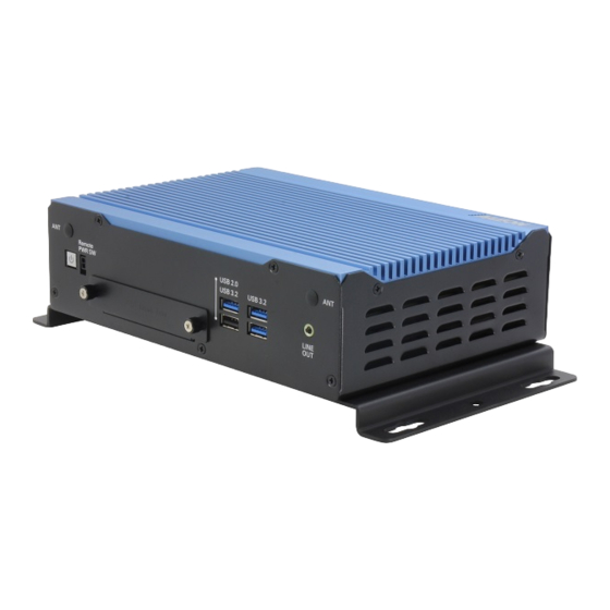
List of Connectors Please refer to the table below for all of the system’s connectors that you can configure for your application Label Function HDMI Dual Port DP Dual Port LAN 1G + USB 2.0 x 2 Connector LAN 2.5G x 2 Connector Reset Switch Wafer Box Remote Button SPI Flash Header... - Page 25 Label Function CN34 COM 6 Wafer Box RS232/RS422/RS485 BAT1 RTC Battery Power Button DIMM1 DDR5 SO-DIMM Slot DIMM2 DDR5 SO-DIMM Slot Chapter 2 – Hardware Information...
-
Page 26: Hdmi Dual Port (Cn1)
2.4.1 HDMI Dual Port (CN1) Pin Name Signal Type Signal level HDMI1_DATA2_P DIFF HDMI1_DATA2_N DIFF HDMI1_DATA1_P DIFF HDMI1_DATA1_N DIFF HDMI1_DATA0_P HDMI1_DATA0_n HDMI1_CLK_P DIFF HDMI1_CLK_N DIFF 3.3V HDMI1_SCL HDMI1_SDA Chapter 2 – Hardware Information... - Page 27 Pin Name Signal Type Signal level +V5S_HDMI_CON HDMI1_HPD HDMI2_DATA2_P HDMI2_DATA2_N HDMI2_DATA1_P HDMI2_DATA1_N HDMI2_DATA0_P HDMI2_DATA0_N HDMI2_CLK_P HDMI2_CLK_N 3.3V HDMI2_SCL HDMI2_SDA +V5S_HDMI_CON HDMI2_HPD Chapter 2 – Hardware Information...
-
Page 28: Dp Dual Port (Cn2)
2.4.2 DP Dual Port (CN2) Signal Signal Type Signal Level DP1_DATA0 _P DIFF DP1_DATA0_N DIFF DP1_DATA1 _P DIFF DP1_DATA1 _N DIFF DP1_DATA2 _P DIFF DP1_DATA1 _N DIFF DP1_DATA3 _P DIFF DP1_DATA3 _N DIFF CONFIG1 3.3V CONFIG2 DP1_AUX _P DIFF DP1_AUX _N DIFF DP1_HPD Chapter 2 –... - Page 29 Signal Signal Type Signal Level RETURN DP1_PWR +3.3V DP2_DATA0 _P DIFF DP2_DATA0_N DIFF DP2_DATA1 _P DIFF DP2_DATA1 _N DIFF DP2_DATA2 _P DIFF DP2_DATA1 _N DIFF DP2_DATA3 _P DIFF DP2_DATA3 _N DIFF CONFIG1 3.3V CONFIG2 DP2_AUX _P DIFF DP2_AUX _N DIFF DP2_HPD RETURN DP2_PWR...
-
Page 30: 2.5Gbe Lan) & Usb 2.0 Connector (Cn3)
2.4.3 RJ-45 (2.5GbE LAN) & USB 2.0 Connector (CN3) Signal Signal Type LAN1_MDI0P DIFF LAN1_MDI0N DIFF LAN1_MDI1P DIFF LAN1_MDI1N DIFF LAN1_MDI2P DIFF LAN1_MDI2N DIFF LAN1_MDI3P DIFF LAN1_MDI3N DIFF Signal Signal Type Signal Level VCC_USB5 USB5- DIFF USB5+ DIFF VCC_USB5 USB6- DIFF Chapter 2 –... -
Page 31: 2.5Gbe Lan) Connector (Cn4)
Signal Signal Type Signal Level USB6+ DIFF 2.4.4 RJ-45 (2.5GbE LAN) Connector (CN4) Signal Signal Type LAN2_MDI0P DIFF LAN2_MDI0N DIFF LAN2_MDI1P DIFF LAN2_MDI1N DIFF LAN2_MDI2P DIFF LAN2_MDI2N DIFF LAN2_MDI3P DIFF LAN2_MDI3N DIFF Chapter 2 – Hardware Information... -
Page 32: Reset Switch Wafer Box (Cn6)
Signal Signal Type LAN3_MDI0P DIFF LAN3_MDI0N DIFF LAN3_MDI1P DIFF LAN3_MDI1N DIFF LAN3_MDI2P DIFF LAN3_MDI2N DIFF LAN3_MDI3P DIFF LAN3_MDI3N DIFF 2.4.5 Reset Switch Wafer Box (CN6) Signal Signal Type HWRST# Chapter 2 – Hardware Information... -
Page 33: Remote Button (Cn7)
2.4.6 Remote Button (CN7) Signal Signal Type PWR_BUTTON# 2.4.7 SPI Flash Header (CN8) Signal Level Signal Signal Type +V3P3M_SPI +3.3V SPI_CE0#_F SPI_CLK_F SPI_SO_F SPI_SI_F Chapter 2 – Hardware Information... -
Page 34: Espi Wafer Box (Debug Port) (Cn9)
2.4.8 eSPI Wafer Box (Debug Port) (CN9) Signal Signal Type Signal Level ESPI_IO_0 +1.8V ESPI_IO_1 +1.8V ESPI_IO_2 +1.8V ESPI_IO_3 +1.8V +3.3V +3.3V ESPI_IO_CS# ESPI_IO_RST# EPSI_IO_LCLK SMCLK SMDAT Chapter 2 – Hardware Information... -
Page 35: Sata Hdd Connector (Cn11)
2.4.9 2.5” SATA HDD Connector (CN11) Signal Level Signal Signal Type SATA0_TXP DIFF SATA0_TXN DIFF SATA0_RXN DIFF SATA0_RXP DIFF +V3P3S +3.3V +V3P3S +3.3V +V3P3S +3.3V +V5S +V5S +V5S Chapter 2 – Hardware Information... -
Page 36: Dio Wafer Box (Cn12)
Signal Signal Type Signal Level +V12S +12V +V12S +12V +V12S +12V 2.4.10 DIO Wafer Box (CN12) DIO0 DIO1 DIO2 DIO3 DIO4 DIO5 DIO6 DIO7 Signal Level Signal Signal Type DIO0 DIO1 DIO2 DIO3 DIO4 DIO5 DIO6 DIO7 Chapter 2 – Hardware Information... -
Page 37: Dual Com Connector Rs232/Rs422/Rs485 (Cn13, Cn27)
2.4.11 Dual COM Connector RS232/RS422/RS485 (CN13, CN27) Pin Name Signal Type RS-422 RS-485 RS422_TX- RS485_D- RS422_TX+ RS485_D+ RS422_RX+ RS422_RX- Chapter 2 – Hardware Information... -
Page 38: 2280 M-Key Slot (Cn14)
2.4.12 M.2 2280 M-Key Slot (CN14) Signal Signal Signal Pin Name Pin Name Type Type Level +V3P3_NGFF +3.3V +V3P3_NGFF +3.3V PCIE4_3_RXN CARD_PWR_OFF_N +3.3V PCIE4_3_RXP PCIE4_3_TXN +V3P3_NGFF +3.3V PCIE4_3_TXP +V3P3_NGFF +3.3V +V3P3_NGFF +3.3V PCIE4_2_RXN +V3P3_NGFF +3.3V PCIE4_2_RXP PCIE4_2_TXN PCIE4_2_TXP PCIE4_1_RXN PCIE4_1_RXP Chapter 2 –... - Page 39 Signal Signal Signal Pin Name Pin Name Type Type Level PCIE4_1_TXN PCIE4_1_TXP DEV_SLP +3.3V SMB_CLK_M2 +1.8V PCIE4_0_RXP SMB_DATA_M2 +1.8V PCIE4_0_RXN PCIE4_0_TXN PCIE4_0_TXP BUF_PLT_RST_R +3.3V PCIE_CLKREQ#0 +3.3V CLKOUT_PCIE_N0 M2_WAKE# +3.3V CLKOUT_PCIE_P0 +V3P3_NGFF +3.3V +V3P3_NGFF +3.3V +V3P3_NGFF +3.3V Chapter 2 – Hardware Information...
-
Page 40: 2230 E-Key Slot (Cn15)
2.4.13 M.2 2230 E-Key Slot (CN15) Signal Signal Signal Pin Pin Name Pin Pin Name Type Type level +V3P3_NGFF_E +3.3V USB_PP9 DIFF +V3P3_NGFF_E +3.3V USB_PN9 DIFF M.2_BT_PCMCLK_C +3.3V M.2_BT_PCMFRM_C +3.3V M.2_BT_PCMIN_C +3.3V M.2_BT_PCMOUT_C +3.3V KEYE_UART_WAKE_N +3.3V PCIE5_TXP DIFF Chapter 2 – Hardware Information... - Page 41 Signal Signal Signal Pin Pin Name Pin Pin Name Type Type level PCIE5_TXN DIFF CL_RST# +3.3V CL_DATA +3.3V PCIE5_RXP DIFF CL_CLK +3.3V PCIE5_RXN DIFF GPPC_F6_CNV_PA_BLANKING +3.3V CNV_MFUART2_TXD +3.3V CLKOUT_PCIE_P4 DIFF CNV_MFUART2_RXD +3.3V CLKOUT_PCIE_N4 DIFF SUSCLK +3.3V BUF_PLT_RST# +3.3V PCIE_CLKREQ#4 GPP_A13_PMC_I2C_SCL +3.3V KEYE_WAKE_N GPPC_E3_CPU_GP_0...
-
Page 42: 3052 B-Key Slot (Cn16)
2.4.14 M.2 3052 B-Key Slot (CN16) Signal Signal Signal Pin Pin Name Pin Pin Name Type Type level +3P3V_NGFF_3052 +3.3V +3P3V_NGFF_3052 +3.3V FULL_CARD_POWER +3.3V USB_PP10 3GPW_EN +3.3V USB_PN10 USB3_RX4_N UIM_RESET USB3_RX4_P UIM_CLK UIM_DATA Chapter 2 – Hardware Information... - Page 43 Signal Signal Signal Pin Pin Name Pin Pin Name Type Type level USB3_TX4_N UIM_PWR1 USB3_TX4_P PCIE12_R-_SATA_R- PCIE12_R+_SATA_R+ PCIE12_T-_SATA_T- PCIE12_T+_SATA_T+ BUF_PLT_3052_RST# +3.3V PCIE_CLKREQ#3 +3.3V CLK_PCIE_N3 M2_3052_WAKE# +3.3V CLK_PCIE_P3 BUF_PLT_3052_RST# SUSCLK_3052 +3P3V_NGFF_3052 +3.3V +3P3V_NGFF_3052 +3.3V +3P3V_NGFF_3052 +3.3V Chapter 2 – Hardware Information...
-
Page 44: Sim Slot (Cn17)
2.4.15 SIM Slot (CN17) Signal Signal Type UIM_PWR UIM_RESET UIM_CLK UIM_VPP UIM_DATA Chapter 2 – Hardware Information... -
Page 45: Usb 3.2 + Usb 2.0 Connector (Cn18)
2.4.16 USB 3.2 + USB 2.0 Connector (CN18) Signal Signal Type Signal Level VCC_USB USB3- DIFF USB3+ DIFF USB3_RX3_N_C DIFF USB3_RX3_P_C DIFF USB3_TX3_N_C DIFF USB3_TX3_P_C DIFF VCC_USB USB4- DIFF USB4+ DIFF Chapter 2 – Hardware Information... -
Page 46: Usb 3.2 X 2 Connector (Cn22)
2.4.17 USB 3.2 x 2 Connector (CN22) Signal Signal Type Signal Level VCC_USB USB1- DIFF USB1+ DIFF USB3_RX1_N_C DIFF USB3_RX1_P_C DIFF USB3_TX1_N_C DIFF USB3_TX1_P_C DIFF VCC_USB USB2- DIFF USB2+ DIFF USB3_RX2_N_C DIFF USB3_RX2_P_C DIFF USB3_TX2_N_C DIFF USB3_TX2_P_C DIFF Chapter 2 – Hardware Information... -
Page 47: Usb 2.0 Wafer Box (Cn20, Cn21)
2.4.18 USB 2.0 Wafer Box (CN20, CN21) Signal Signal Type Signal Level USBD- DIFF USBD+ DIFF Chapter 2 – Hardware Information... -
Page 48: Audio Connector (Cn23)
2.4.19 Audio Connector (CN23) Signal Level Signal Signal Type AUD_GND LOUT_R +VDD_AUD HP_DET_3 LOUT_L 2.4.20 Phoenix Connector Power Input (CN25) Signal Signal Type Signal Level +9V ~ +36V Chapter 2 – Hardware Information... -
Page 49: Com5/Com6 Wafer Box (Optional) (Cn33, Cn34)
2.4.21 COM5/COM6 Wafer Box (Optional) (CN33, CN34) Pin Name Signal Type RS-422 RS-485 RS422_TX- RS485_D- RS422_TX+ RS485_D+ RS422_RX+ RS422_RX- Chapter 2 – Hardware Information... -
Page 50: Rtc Battery (Bat1)
2.4.22 RTC Battery (BAT1) Signal Signal Type Signal Level +V3P3A_RTC +3.3V 2.4.23 Power Button (SW1) Signal Level Signal Signal Type PWR_BUTTON# Chapter 2 – Hardware Information... - Page 51 Signal Signal Type Signal Level PWR_BUTTON# +V5S Chapter 2 – Hardware Information...
-
Page 52: Hardware Installation
Hardware Installation 2.5.1 2.5” HDD Installation For this process you will need a Phillips head screwdriver. Step 1: Locate the removable 2.5” SATA Drive Bay on the front I/O side of the chassis. Step 2: Unscrew the outer pins and remove the 2.5” SATA Drive Bay from the chassis. Step 3: Unscrew the four (4) screws at each corner of the 2.5”... -
Page 53: Ddr5 Sodimm Installation
2.5.2 DDR5 SODIMM Installation For this process you will need a Phillips head screwdriver. Step 1: Access the DDR5 SODIMM slots by removing the two (2) screws on the panel marked ‘SODIMM/M.2 2280’ on the bottom-side of the chassis as shown below. Step 2: Insert thermal pad followed by DDR5 SODIMM(s). -
Page 54: Nvme Storage Module (M.2 2280 M-Key) Installation
2.5.3 NVMe Storage Module (M.2 2280 M-Key) Installation For this process you will need a Phillips head screwdriver. Step 1: Access the M.2 2280 M-Key slot by removing the two (2) screws on the panel marked ‘SODIMM/M.2 2280’ on the bottom-side of the chassis as shown below. Step 2: Insert NVMe Storage Module. -
Page 55: Wi Fi Module (M.2 2230 E-Key Slot) Installation
2.5.4 Wi Fi Module (M.2 2230 E-Key Slot) Installation For this process you will need a Phillips head screwdriver. Step 1: Access the M.2 2230 E-Key slot by removing the screw on the panel marked ‘M.2 2230’ on the bottom-side of the chassis as shown below. Step 2: Insert Wi-Fi Module. -
Page 56: Module (M.2 3052 B-Key Slot) Installation
2.5.5 5G Module (M.2 3052 B-Key Slot) Installation For this process you will need a Phillips head screwdriver. Step 1: Access the M.2 3052 B-Key slot by removing the 2.5” drive bay, then remove the screw on the panel marked ‘M.2 3052’ on the bottom-side of the chassis as shown below. -
Page 57: Chapter 3 - Ami Bios Setup
Chapter 3 Chapter 3 - AMI BIOS Setup... -
Page 58: System Test And Initialization
System Test and Initialization The system uses certain routines to perform testing and initialization. If an error, fatal or non-fatal, is encountered, a few short beeps or an error message will be outputted. The board can usually continue the boot up sequence with non-fatal errors. The system configuration verification routines check the current system configuration against the values stored in the CMOS memory. -
Page 59: Ami Bios Setup
AMI BIOS Setup The AMI BIOS ROM has a pre-installed Setup program that allows users to modify basic system configurations, which is stored in the battery-backed CMOS RAM and BIOS NVRAM so that the information is retained when the power is turned off. To enter BIOS Setup, press... -
Page 60: Setup Submenu: Main
Setup Submenu: Main Chapter 3 – AMI BIOS Setup... -
Page 61: Setup Submenu: Advanced
Setup Submenu: Advanced Chapter 3 – AMI BIOS Setup... -
Page 62: Cpu Configuration
3.4.1 CPU Configuration Options Summary Intel (VMX) Disabled Virtualization Enabled Optimal Default, Failsafe Default Technology When enabled, a VMM can utilize the additional hardware capabilities provided by Vanderpool Technology. Hyper-Threading Disabled Enabled Optimal Default, Failsafe Default Enable or Disable Hyper-Threading Technology Intel®... -
Page 63: Memory Configuration
Options Summary C states Disabled Enabled Optimal Default, Failsafe Default Enable/Disable CPU Power Management. Allows CPU to go to C states when it’s not 100% utilized. 3.4.2 Memory Configuration Chapter 3 – AMI BIOS Setup... -
Page 64: Pch-Fw Configuration
3.4.3 PCH-FW Configuration Options Summary AMT BIOS Features Enabled Optimal Default, Failsafe Default Disabled When disabled AMT BIOS Features are no longer supported and user is no longer able to access MEBx Setup. Note: This option does not disable Manageability Features in FW. Chapter 3 –... -
Page 65: Firmware Update Configuration
3.4.3.1 Firmware Update Configuration Options Summary Me FW Image Enabled Re-Flash Disabled Optimal Default, Failsafe Default Enable/ Disable Me FW Image Re-Flash function. FW Update Enabled Disabled Optimal Default, Failsafe Default Enable/ Disable Me FW Update function. Chapter 3 – AMI BIOS Setup... -
Page 66: Hardware Monitor
3.4.4 Hardware Monitor Options Summary Smart Fan Enabled Optimal Default, Failsafe Default Disabled Enable or Disable Smart Fan Chapter 3 – AMI BIOS Setup... -
Page 67: Smart Fan Mode Configuration
3.4.5 Smart Fan Mode Configuration Options Summary FAN1 Output Output PWM mode (open drain) Optimal Default, Failsafe Default Mode Linear Fan Application Output PWM mode (push pull) Output PWM mode (push pull) to control 4-wire fans. Linear fan application circuit to control 3-wire fan speed by fan’s power terminal. - Page 68 Options Summary Temperature 1 Optimal Default, Failsafe Default Temperature 2 Optimal Default, Failsafe Default Temperature 3 Optimal Default, Failsafe Default Temperature 4 Optimal Default, Failsafe Default Temperature 5 Optimal Default, Failsafe Default Duty Cycle 1 Optimal Default, Failsafe Default Duty Cycle 2 Optimal Default, Failsafe Default Duty Cycle 3 Optimal Default, Failsafe Default...
-
Page 69: Fan 1 Smart Fan Control (Auto Rpm Mode)
3.4.5.1 Fan 1 Smart Fan Control (Auto RPM Mode) Options Summary Fan 1 Smart Fan Auto RPM Mode Control Smart Fan Mode Select. Temperature CPU Temperature Optimal Default, Failsafe Default Source System Temperature System Temperature 2 Select the monitored temperature source for this fan. Temperature 1 Optimal Default, Failsafe Default Temperature 2... -
Page 70: Fan 1 Smart Fan Control (Manual Duty Mode)
Options Summary RPM Percentage 5 40 Optimal Default, Failsafe Default Auto fan speed control. Fan speed will follow different temperature by different RPM 1-100 3.4.5.2 Fan 1 Smart Fan Control (Manual Duty Mode) Options Summary Fan 1 Smart Fan Manual Duty Mode Control Smart Fan Mode Select. -
Page 71: Fan 1 Smart Fan Control (Manual Rpm Mode)
3.4.5.3 Fan 1 Smart Fan Control (Manual RPM Mode) Options Summary Fan 1 Smart Fan Manual RPM Mode Control Smart Fan Mode Select. Temperature CPU Temperature Optimal Default, Failsafe Default Source System Temperature System Temperature 2 Select the monitored temperature source for this fan. Manual RPM 3000 Optimal Default, Failsafe Default... -
Page 72: Power Management
3.4.6 Power Management Options Summary Power Mode ATX Type Optimal Default, Failsafe Default AT Type Select system power mode Restore AC Power Last State Optimal Default, Failsafe Default Loss Always On Always Off Set GPI [3:0] Output as Hi or Low System Wake On Disabled Optimal Default, Failsafe Default... -
Page 73: Aaeon Bios Robot
3.4.7 AAEON BIOS Robot Options Summary Sends watch dog Disabled Optimal Default, Failsafe Default before BIOS POST Enabled Enabled – Robot set Watch Dog Timer (WDT) right after power on, before BIOS start POST process. And then Robot will clear WDT on completion of POST. WDT on completion of POST. -
Page 74: Device Detecting Configuration
Options Summary Enabled -Robot holds BIOS from starting POST, right after power on. This allows BIOS POST to start with stable power or start after system is physically warmed-up. Note: Robot does this before 'Sends watch dog'. Delayed POST Disabled Optimal Default, Failsafe Default (DXE phase) Enabled... - Page 75 Options Summary Retry-Count Optimal Default, Failsafe Default Fill retry counter here. Robot will reset system at most counter times, and then let system continue its POST. At time After shoe logo Optimal Default, Failsafe Default Before show logo Select robot action time: After show logo -Robot will do action after logo is displayed. System devices are almost ready.
- Page 76 Options Summary MMIO Select interface robot should use to communicate with device 3.4.7.1.2 Device #2 Detecting Configuration Options Summary Interface Disabled Optimal Default, Failsafe Default SMBUS Legacy I/O Super I/O MMIO Select interface robot should use to communicate with device Chapter 3 –...
- Page 77 3.4.7.1.3 Device #3 Detecting Configuration Options Summary Interface Disabled Optimal Default, Failsafe Default SMBUS Legacy I/O Super I/O MMIO Select interface robot should use to communicate with device Chapter 3 – AMI BIOS Setup...
- Page 78 3.4.7.1.4 Device #4 Detecting Configuration Options Summary Interface Disabled Optimal Default, Failsafe Default SMBUS Legacy I/O Super I/O MMIO Select interface robot should use to communicate with device Chapter 3 – AMI BIOS Setup...
- Page 79 3.4.7.1.5 Device #5 Detecting Configuration Options Summary Interface Disabled Optimal Default, Failsafe Default SMBUS Legacy I/O Super I/O MMIO Select interface robot should use to communicate with device Chapter 3 – AMI BIOS Setup...
-
Page 80: Setup Submenu: System I/O
Setup Submenu: System I/O Chapter 3 – AMI BIOS Setup... -
Page 81: Storage Configuration
3.5.1 Storage Configuration Options Summary SATA Controller(s) Enabled Optimal Default, Failsafe Default Disabled Enable/Disable to SATA Device Chapter 3 – AMI BIOS Setup... -
Page 82: Hd Audio Configuration
3.5.2 HD Audio Configuration Options Summary HD Audio Disabled Enabled Optimal Default, Failsafe Default Control Detection of the HD-Audio device. Disabled = HDA will be unconditionally disabled Enabled = HDA will be unconditionally enabled. Chapter 3 – AMI BIOS Setup... -
Page 83: Digital Io Port Configuration
3.5.3 Digital IO Port Configuration Options Summary DIO1 Input Output Optimal Default, Failsafe Default Set DIO as Input or Output Output Level High Optimal Default, Failsafe Default Set output level when DIO pin is output DIO2 Input Output Optimal Default, Failsafe Default Set DIO as Input or Output Output Level High... - Page 84 Options Summary Output Level High Optimal Default, Failsafe Default Set output level when DIO pin is output DIO4 Input Output Optimal Default, Failsafe Default Set DIO as Input or Output Output Level High Optimal Default, Failsafe Default Set output level when DIO pin is output DIO5 Input Optimal Default, Failsafe Default...
-
Page 85: Legacy Logical Devices Configuration
3.5.4 Legacy Logical Devices Configuration Options Summary DIO1 Input Output Optimal Default, Failsafe Default Set DIO as Input or Output Output Level High Optimal Default, Failsafe Default Set output level when DIO pin is output DIO2 Input Output Optimal Default, Failsafe Default Chapter 3 –... -
Page 86: Serial Port 1
3.5.4.1 Serial Port 1 Options Summary Use This Device Disabled Enabled Optimal Default, Failsafe Default Enable or Disable this Logical Device Possible: Use Automatic Settings Optimal Default, Failsafe Default IO=3F8; IRQ=4; IO=2F8; IRQ=3; Allows the user to change the device resource settings. New settings will be reflected on this setup page after system restarts. -
Page 87: Serial Port 2
3.5.4.2 Serial Port 2 Options Summary Use This Device Disabled Enabled Optimal Default, Failsafe Default Enable or Disable this Logical Device Possible: Use Automatic Settings Optimal Default, Failsafe Default IO=2F8; IRQ=3; IO=3F8; IRQ=4; Allows the user to change the device resource settings. New settings will be reflected on this setup page after system restarts. -
Page 88: Serial Port 3
3.5.4.3 Serial Port 3 Options Summary Use This Device Disabled Enabled Optimal Default, Failsafe Default Enable or Disable this Logical Device Possible: Use Automatic Settings Optimal Default, Failsafe Default IO=3E8; IRQ=11; IO=2E8; IRQ=11; Allows the user to change the device resource settings. New settings will be reflected on this setup page after system restarts. -
Page 89: Serial Port 4
3.5.4.4 Serial Port 4 Options Summary Use This Device Disabled Enabled Optimal Default, Failsafe Default Enable or Disable this Logical Device Possible: Use Automatic Settings Optimal Default, Failsafe Default IO=2E8; IRQ=11; IO=3E8; IRQ=11; Allows the user to change the device resource settings. New settings will be reflected on this setup page after system restarts. -
Page 90: Serial Port 5
3.5.4.5 Serial Port 5 Options Summary Use This Device Disabled Enabled Optimal Default, Failsafe Default Enable or Disable this Logical Device Possible: Use Automatic Settings Optimal Default, Failsafe Default IO=2D0; IRQ=11; IO=2C0; IRQ=11; Allows the user to change the device resource settings. New settings will be reflected on this setup page after system restarts. -
Page 91: Serial Port 6
3.5.4.6 Serial Port 6 Options Summary Use This Device Disabled Enabled Optimal Default, Failsafe Default Enable or Disable this Logical Device Possible: Use Automatic Settings Optimal Default, Failsafe Default IO=2C0; IRQ=11; IO=2D0; IRQ=11; Allows the user to change the device resource settings. New settings will be reflected on this setup page after system restarts. -
Page 92: Serial Port Console Redirection
3.5.5 Serial Port Console Redirection Options Summary Console Disabled Optimal Default, Failsafe Default Redirection Enabled Console Redirection Enable or Disable Console Disabled Optimal Default, Failsafe Default Redirection EMS Enabled Console Redirection Enable or Disable Chapter 3 – AMI BIOS Setup... -
Page 93: Console Redirection Settings (Com0)
3.5.5.1 Console Redirection Settings (COM0) Options Summary Terminal Type VT100 VT100Plus VT-UTF8 ANSI Optimal Default, Failsafe Default Emulation: ANSI: Extended ASCII char set. VT100: ASCII char set. VT100Plus: Extends VT100 to support color, function keys, etc. VT-UTF8: Uses UTF8 encoding to map Unicode chars onto 1 or more bytes. - Page 94 Options Summary Data Bits Parity None Optimal Default, Failsafe Default Even Mark Space A parity bit can be sent with the data bits to detect some transmission errors. Even: parity bit is 0 if the num of 1's in the data bits is even. Odd: parity bit is 0 if num of 1's in the data bits is odd.
-
Page 95: Console Redirection Settings (Out-Of-Band Mgmt Port)
3.5.5.2 Console Redirection Settings (Out-of-Band Mgmt Port) Options Summary Out-of-Band Mgmt COM0 Optimal Default, Failsafe Default Port COM1(Pci Bus0, Dev0, Func0) (Disabled) Microsoft Windows Emergency Management Services (EMS) allows for remote management of a Windows Server OS through a serial port. Terminal Type EMS VT100 VT100Plus VT-UTF8... - Page 96 Options Summary Selects serial port transmission speed. The speed must be matched on the other side. Long or noisy lines may require lower speeds. Flow Control EMS None Optimal Default, Failsafe Default Hardware RTS/CTS Software Xon/Xoff Flow control can prevent data loss from buffer overflow. When sending data, if the receiving buffers are full, a 'stop' signal can be sent to stop the data flow.
-
Page 97: Setup Submenu: Security
Setup Submenu: Security Change User/Administrator Password You can set a User Password once an Administrator Password. The password will be required during boot up, or when the user enters the Setup utility. Please Note that a User Password does not provide access to many of the features in the Setup utility. Select the password you wish to set, press Enter to open a dialog box to enter your password (you can enter no more than six letters or numbers). -
Page 98: Trusted Computing
3.6.1 Trusted Computing Options Summary Security Device Enable Optimal Default, Failsafe Default Support Disable Enables or Disables BIOS support for security device. O.S. will not show Security Device. TCG EFI protocol and INT1A interface will not be available. SHA256 PCR Bank Disabled Enabled Optimal Default, Failsafe Default Enable or Disable SHA256 PCR Bank... - Page 99 Options Summary Enable or Disable Platform Hierarchy Storage Hierarchy Disabled Enabled Optimal Default, Failsafe Default Enable or Disable Storage Hierarchy Endorsement Disabled Hierarchy Enabled Optimal Default, Failsafe Default Enable or Disable Endorsement Hierarchy Physical Presence Spec Version Optimal Default, Failsafe Default Select to Tell O.S.
-
Page 100: Secure Boot
3.6.2 Secure Boot Options Summary Secure Boot Disabled Optimal Default, Failsafe Default Enabled Secure Boot feature is Active if Secure Boot is Enabled, Platform Key (PK) is enrolled and the System is in User mode. The mode change requires platform reset Secure Boot Mode Standard Custom Optimal Default, Failsafe Default... -
Page 101: Key Management
3.6.2.1 Key Management Options Summary Factory Key Disabled Optimal Default, Failsafe Default Provision Enabled Install factory default Secure Boot keys after the platform reset and while the System is in Setup mode Restore Factory Keys Force System to User Mode. Install factory default Secure Boot key databases. Enroll Efi Image Allow Efi image to run in Secure Boot mode. - Page 102 Options Summary Forbidden Update Signatures (dbx) Append Authorized Update TimeStamps (dbt) Append OsRecovery Update Signatures (dbr) Append Enroll Factory Defaults or load certificates from a file: 1. Public Key Certificate: EFI_SIGNATURE_LIST EFI_CERT_X509 (DER) EFI_CERT_RSA2048 (bin) EFI_CERT_SHAXXX 2.Authenticated UEFI Variable 3.EFI PE/COFF Image (SHA256) Key Source: Factory, External, Mixed Chapter 3 –...
-
Page 103: Setup Submenu: Boot
Setup Submenu: Boot Options Summary Quiet Boot Disabled Enabled Default Enables/disables Quiet Boot option. Network Stack Disabled Default Enabled Enable/Disable UEFI Network Stack. Boot Option #1 Hard Disk Boot Option #2 NVME Boot Option #3 USB Device Boot Option #4 Network Sets the system boot order Chapter 3 –... -
Page 104: Uefi Bbs Priorities
3.7.1 UEFI BBS Priorities Options Summary Quiet Boot Disabled Enabled Default Enables/disables Quiet Boot option. Network Stack Disabled Default Enabled Enable/Disable UEFI Network Stack. Boot Option #1 Hard Disk Boot Option #2 NVME Boot Option #3 USB Device Boot Option #4 Network Sets the system boot order Chapter 3 –... -
Page 105: Setup Submenu: Save & Exit
Setup Submenu: Save & Exit Chapter 3 – AMI BIOS Setup... -
Page 106: Setup Submenu: Mebx
Setup Submenu: MEBx Chapter 3 – AMI BIOS Setup... -
Page 107: Chapter 4 - Drivers Installation
Chapter 4 Chapter 4 – Drivers Installation... -
Page 108: Drivers Download And Installation
Drivers Download and Installation Drivers for the BOXER-6646-ADP can be downloaded from the product page on the AAEON website by following this link: https://www.aaeon.com/en/p/compact-fanless-box-pc-solutions-boxer-6646-adp Chapter 4 – Drivers Installation... -
Page 109: Appendix A - I/O Information
Appendix A Appendix A – I/O Information... -
Page 110: I/O Address Map
I/O Address Map Appendix A – I/O Information... - Page 111 Appendix A – I/O Information...
-
Page 112: A.2 Memory Address Map
A.2 Memory Address Map Appendix A – I/O Information... -
Page 113: A.3 Irq Mapping Chart
A.3 IRQ Mapping Chart Appendix A – I/O Information...