
Related Manuals for Asus Aaeon BOXER-6641


Summary of Contents for Asus Aaeon BOXER-6641
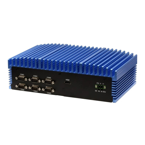
- Page 1 BOXER-6641 Fanless Embedded Box PC User’s Manual 5 Last Updated: March 24, 2021...
- Page 2 Copyright Notice This document is copyrighted, 2021. All rights are reserved. The original manufacturer reserves the right to make improvements to the products described in this manual at any time without notice. No part of this manual may be reproduced, copied, translated, or transmitted in any form or by any means without the prior written permission of the original manufacturer.
- Page 3 Acknowledgement All other product name or trademarks are properties of their respective owners. Microsoft Windows® is a registered trademark of Microsoft Corp. ⚫ Intel®, Pentium®, Celeron®, and Xeon® are registered trademarks of Intel ⚫ Corporation Intel Core™ is a trademark of Intel Corporation ⚫...
- Page 4 Packing List Before setting up your product, please make sure the following items have been shipped: Item Quantity BOXER-6641 ⚫ Wallmount bracket ⚫ Screw Package ⚫ 3 Pin DC-In Power Connector ⚫ If any of these items are missing or damaged, please contact your distributor or sales representative immediately.
- Page 5 About this Document This User’s Manual contains all the essential information, such as detailed descriptions and explanations on the product’s hardware and software features (if any), its specifications, dimensions, jumper/connector settings/definitions, and driver installation instructions (if any), to facilitate users in setting up their product. Users may refer to the product page at AAEON.com for the latest version of this document.
- Page 6 Safety Precautions Please read the following safety instructions carefully. It is advised that you keep this manual for future references All cautions and warnings on the device should be noted. Make sure the power source matches the power rating of the device. Position the power cord so that people cannot step on it.
- Page 7 If any of the following situations arises, please the contact our service personnel: Damaged power cord or plug Liquid intrusion to the device iii. Exposure to moisture Device is not working as expected or in a manner as described in this manual The device is dropped or damaged Any obvious signs of damage displayed on the device...
- Page 8 FCC Statement This device complies with Part 15 FCC Rules. Operation is subject to the following two conditions: (1) this device may not cause harmful interference, and (2) this device must accept any interference received including interference that may cause undesired operation. Caution: There is a danger of explosion if the battery is incorrectly replaced.
- Page 9 China RoHS Requirements (CN) 产品中有毒有害物质或元素名称及含量 AAEON System QO4-381 Rev.A0 有毒有害物质或元素 部件名称 铅 汞 镉 六价铬 多溴联苯 多溴二苯 醚(PBDE) (Pb) (Hg) (Cd) (Cr(VI)) (PBB) 印刷电路板 × ○ ○ ○ ○ ○ 及其电子组件 外部信号 × ○ ○ ○ ○ ○ 连接器及线材 ○ ○...
- Page 10 China RoHS Requirement (EN) Hazardous and Toxic Materials List AAEON System QO4-381 Rev.A0 Hazardous or Toxic Materials or Elements Component Name PCB and Components Wires & Connectors for Ext.Connections Chassis CPU & RAM HDD Drive LCD Module Optical Drive Touch Control Module Battery This form is prepared in compliance with the provisions of SJ/T 11364.
-
Page 11: Table Of Contents
Table of Contents Chapter 1 - Product Specifications ..................1 Specifications ......................2 Chapter 2 – Hardware Information ..................4 BOXER-6641 Dimensions ..................5 Jumpers and Connectors ..................9 List of Jumpers ......................11 2.3.1 Setting Jumpers ..................11 2.3.2 ATX/ AT Mode Selection (JP19) ............ - Page 12 2.4.17 Audio Connector (CN18) ..............34 2.4.18 SPI Flash Port (CN7) ................35 2.4.19 SATA Port (SATA 1,2,3,4) ............... 35 2.4.20 USB2.0 Wafer BOX (5P Pitch: 1.25mm) (CN 45,71,72) ....36 2.4.21 SATA PWR (PWR 1,2,3,4) ..............36 2.4.22 DC-IN Connector (CN23) ..............37 2.4.23 LAN (RJ-45) + Dual USB3.2 Gen 1 (CN74) ........
- Page 13 3.4.6 Advanced: Hardware Monitor ............70 3.4.7 Advanced: SIO Configuration ............. 71 3.4.7.1 Serial Port 1 Configuration ............ 72 3.4.7.2 Serial Port 2 Configuration ........... 73 3.4.7.3 Serial Port 3 Configuration ........... 74 3.4.7.4 Serial Port 4 Configuration ........... 75 3.4.7.5 Serial Port 5 Configuration ...........
- Page 14 DIO Programming ....................112 Digital I/O Register....................113 Digital I/O Sample Program................115 Preface...
-
Page 15: Chapter 1 - Product Specifications
Chapter 1 Chapter 1 - Product Specifications... -
Page 16: Specifications
Specifications System Intel® Xeon® E-2124G (A2 & A6 models only) Intel® i9-9900T Intel® i7-9700TE Intel® i7-8700T Intel® i5-8500T Intel®i3-8100T Pentium® G5400T Celeron® G4900T Intel® C246/H310 Chipset DDR4-2666 SO-DIMM slot x 2, System Memory Up to 64GB, ECC or Non-ECC Supported HDMI x 2 Display Interface 2.5”... - Page 17 System HDD LED x 1 Indicator SYS LED x 1 Windows® 10 64-bit OS Support Linux Ubuntu 18.04 Power Supply Power Requirement 3-pin DC Input 10~35V Mechanical Mounting Wall mount Dimensions (W x H x D) 10.4” x 3.19” x 6.15” (264.2mm x 80.92mm x 156.2mm) Gross Weight 10.4 lbs.
-
Page 18: Chapter 2 - Hardware Information
Chapter 2 Chapter 2 – Hardware Information... -
Page 19: Boxer-6641 Dimensions
BOXER-6641 Dimensions BOXER-6641-A1/A5 (H310 Chipset) Chapter 2 – Hardware Information... - Page 20 Chapter 2 – Hardware Information...
- Page 21 BOXER-6641-A2/A6 (C246 Chipset) Chapter 2 – Hardware Information...
- Page 22 Chapter 2 – Hardware Information...
-
Page 23: Jumpers And Connectors
Jumpers and Connectors Note: Board dimensions are 225mm x 151.5mm x 1.8mm Chapter 2 – Hardware Information... - Page 24 Chapter 2 – Hardware Information...
-
Page 25: List Of Jumpers
List of Jumpers Please refer to the table below for all of the system’s jumpers that you can configure for your application. Label Function JP19 ATX/AT Mode Selection JP24 CMOS Control Selection (Clear CMOS) 2.3.1 Setting Jumpers The BOXER-6641 comes with several jumpers which allow you to configure the system by either setting the jumper to “open”... -
Page 26: Atx/ At Mode Selection (Jp19)
2.3.2 ATX/ AT Mode Selection (JP19) ATX (default) Note: Disable Auto Power Button JP19 (1-2) requires user to use power button JP19 (1-2) to power on the system. 2.3.3 CMOS Control Selection (JP24) 1 2 3 Normal (Default) Clear CMOS Chapter 2 –... -
Page 27: List Of Connectors
List of Connectors Please refer to the table below for all of the system’s connectors that you can configure for your application Label Function BAT1 RTC Battery SPI flash port PCIE [x4] Slot CN14 LAN+USB3.2 Gen 1 x2 Connector CN15 LAN+USB3.2 Gen 1 x2 Connector CN17 Audio Wafer... - Page 28 Label Function CN74 LAN+USB3.2 Gen 1 x2 Connector (USB2.0x2 for H310 Chipset) CN75 HDMI Port CN76 HDMI Port LPC1 LPC Port PCIE1 Mini-PCIE slot PCIE2 Mini-PCIE slot PWR1 SATA PWR Connector PWR2 SATA PWR Connector PWR3 SATA PWR Connector PWR4 SATA PWR Connector SATA1 SATA1...
-
Page 29: Hdmi Port (Cn75)
2.4.1 HDMI Port (CN75) Signal Level Signal Signal Type HDMI2_DATA2_P DIFF HDMI2_DATA2_N DIFF HDMI2_DATA1_P DIFF HDMI2_DATA1_N DIFF HDMI2_DATA0_P DIFF HDMI2_DATA0_N DIFF HDMI2_CLK_P DIFF HDMI2_CLK_N Chapter 2 – Hardware Information... -
Page 30: Hdmi Port (Cn76)
2.4.2 HDMI Port (CN76) Signal Signal Type Signal Level HDMI2_DATA2_P DIFF HDMI2_DATA2_N DIFF HDMI2_DATA1_P DIFF HDMI2_DATA1_N DIFF HDMI2_DATA0_P DIFF HDMI2_DATA0_N DIFF HDMI2_CLK_P DIFF HDMI2_CLK_N Chapter 2 – Hardware Information... -
Page 31: Com Port 1 (Wafer Box, Optional) (Cn59)
2.4.3 COM Port 1 (Wafer Box, Optional) (CN59) Signal Signal Type Signal Level DCD1 DSR1 RTS1 ±9V ±9V CTS1 DTR1 ±9V Chapter 2 – Hardware Information... -
Page 32: Com Port 2 (Wafer Box, Optional) (Cn57)
2.4.4 COM Port 2 (Wafer Box, Optional) (CN57) Signal Signal Type Signal Level DCD2 DSR2 RTS2 ±9V ±9V CTS2 DTR2 ±9V Chapter 2 – Hardware Information... -
Page 33: Com Port 3 (Wafer Box, Optional) (Cn61)
2.4.5 COM Port 3 (Wafer Box, Optional) (CN61) Signal Signal Type Signal Level DCD3 DSR3 RTS3 ±9V ±9V CTS3 DTR3 ±9V Chapter 2 – Hardware Information... -
Page 34: Com Port 4 (Wafer Box, Optional) (Cn55)
2.4.6 COM Port 4 (Wafer Box, Optional) (CN55) Signal Signal Type Signal Level DCD4 DSR4 RTS4 ±9V ±9V CTS4 DTR4 ±9V Chapter 2 – Hardware Information... -
Page 35: Com Port 5 (Wafer Box, Optional) (Cn48)
2.4.7 COM Port 5 (Wafer Box, Optional) (CN48) Signal Signal Type Signal Level DCD5 DSR5 RTS5 ±9V ±9V CTS5 DTR5 ±9V Chapter 2 – Hardware Information... -
Page 36: Com Port 6 (Wafer Box, Optional) (Cn50)
2.4.8 COM Port 6 (Wafer Box, Optional) (CN50) Signal Signal Type Signal Level DCD6 DSR6 RTS6 ±9V ±9V CTS6 DTR6 ±9V Chapter 2 – Hardware Information... -
Page 37: Com1 + Com2 Connector Rs232/Rs422/Rs485 (Cn60)
2.4.9 COM1 + COM2 Connector RS232/RS422/RS485 (CN60) RS232 RS422 RS485 Top Port Bottom Port Chapter 2 – Hardware Information... -
Page 38: Com3 + Com4 Connector Rs232/Rs422/Rs485 (Cn62)
2.4.10 COM3 + COM4 Connector RS232/RS422/RS485 (CN62) RS232 RS422 RS485 Top Port Bottom Port Chapter 2 – Hardware Information... -
Page 39: Com5 + Com6 Connector Rs232/Rs422/Rs485 (Cn49)
2.4.11 COM5 + COM6 Connector RS232/RS422/RS485 (CN49) RS232 RS422 RS485 Top Port Bottom Port Chapter 2 – Hardware Information... -
Page 40: Mini-Card Slot (Full Mini-Card) (Pcie1)
2.4.12 Mini-Card Slot (Full Mini-Card) (PCIE1) Signal Signal Type Signal Level PCIE_WAKE# +3.3V +3.3V +1.5V +1.5V PCIE_CLK_REQ# PCIE_REF_CLK- DIFF PCIE_REF_CLK+ DIFF Chapter 2 – Hardware Information... - Page 41 Signal Signal Type Signal Level W_DISABLE# +3.3V PCIE_RST# +3.3V PCIE_RX- DIFF +3.3VSB +3.3V PCIE_RX+ DIFF +1.5V +1.5V SMB_CLK +3.3V PCIE_TX- DIFF SMB_DATA +3.3V PCIE_TX+ DIFF USB_D- DIFF USB_D+ DIFF +3.3VSB +3.3V +3.3VSB +3.3V Chapter 2 – Hardware Information...
-
Page 42: Mini-Card Slot (Full Mini-Card) (Pcie2)
Signal Signal Type Signal Level +1.5V +1.5V +3.3VSB +3.3V 2.4.13 Mini-Card Slot (Full Mini-Card) (PCIE2) Signal Signal Type Signal Level PCIE_WAKE# +3.3V +3.3V +1.5V +1.5V PCIE_CLK_REQ# Chapter 2 – Hardware Information... - Page 43 Signal Signal Type Signal Level PCIE_REF_CLK- DIFF PCIE_REF_CLK+ DIFF W_DISABLE# +3.3V PCIE_RST# +3.3V PCIE_RX- DIFF +3.3VSB +3.3V PCIE_RX+ DIFF +1.5V +1.5V SMB_CLK +3.3V PCIE_TX- DIFF SMB_DATA +3.3V PCIE_TX+ DIFF Chapter 2 – Hardware Information...
- Page 44 Signal Signal Type Signal Level USB_D- DIFF USB_D+ DIFF +3.3VSB +3.3V +3.3VSB +3.3V +1.5V +1.5V +3.3VSB +3.3V Chapter 2 – Hardware Information...
-
Page 45: Digital Io Port (Cn43)
2.4.14 Digital IO Port (CN43) Signal Level Signal Signal Type DIO0 DIO1 DIO2 DIO3 DIO4 DIO5 DIO6 DIO7 Chapter 2 – Hardware Information... -
Page 46: Lpc Port (Lpc1)
2.4.15 LPC Port (LPC1) Signal Level Signal Signal Type LAD0 +3.3V LAD1 +3.3V LAD2 +3.3V LAD3 +3.3V +3.3V +3.3V LFRAME# LRESET# +3.3V LCLK LDRQ0 LDRQ1 SERIRQ +3.3V Chapter 2 – Hardware Information... -
Page 47: Audio I/O Port (10P Pitch: 1.25Mm) (Cn17)
2.4.16 Audio I/O Port (10P Pitch: 1.25mm) (CN17) Signal Level Signal Signal Type MIC_L MIC_R GND_AUDIO LINE_L_IN LINE_R_IN GND_AUDIO LEFT_OUT GND_AUDIO RIGHT_OUT +5V_AUDIO Chapter 2 – Hardware Information... -
Page 48: Audio Connector (Cn18)
2.4.17 Audio Connector (CN18) Signal Level Signal Signal Type AUD_GND LOUT_L LOUT_R HP_DET_3 HP_DET_4 MIC_L MIC_R HP_DET_1 HP_DET2 Chapter 2 – Hardware Information... -
Page 49: Spi Flash Port (Cn7)
2.4.18 SPI Flash Port (CN7) Signal Signal Type Signal Level SPI_MISO SPI_CLK +3.3VSB +3.3V SPI_MOSI SPI_CS 2.4.19 SATA Port (SATA 1,2,3,4) Signal Level Signal Signal Type SATA_TX+ DIFF SATA_TX- DIFF SATA_RX- DIFF SATA_RX+ DIFF Chapter 2 – Hardware Information... -
Page 50: Usb2.0 Wafer Box (5P Pitch: 1.25Mm) (Cn 45,71,72)
2.4.20 USB2.0 Wafer BOX (5P Pitch: 1.25mm) (CN 45,71,72) Signal Level Signal Signal Type USBD- DIFF USBD+ DIFF 2.4.21 SATA PWR (PWR 1,2,3,4) Signal Level Signal Signal Type +12V +12V Chapter 2 – Hardware Information... -
Page 51: Dc-In Connector (Cn23)
2.4.22 DC-IN Connector (CN23) Signal Level Signal Signal Type +10V~+35V GND_EARTH 2.4.23 LAN (RJ-45) + Dual USB3.2 Gen 1 (CN74) Signal Signal Type Signal Level MDI0+ DIFF MDI0- DIFF MDI1+ DIFF MDI2+ DIFF MDI2- DIFF MDI1- DIFF Chapter 2 – Hardware Information... - Page 52 Signal Signal Type Signal Level MDI3+ DIFF MDI3- DIFF Note: USB2.0x2 for H310 Chipset Signal Level Signal Signal Type +5VSB USB1_D- DIFF USB1_D+ DIFF USB1_SSRX− DIFF USB1_SSRX+ DIFF USB1_SSTX− DIFF USB1_SSTX+ DIFF +5VSB USB2_D- DIFF USB2_D+ DIFF USB2_SSRX− DIFF Chapter 2 – Hardware Information...
-
Page 53: Lan (Rj-45) + Dual Usb3.2 Gen 1 (Cn73)
Signal Signal Type Signal Level USB2_SSRX+ DIFF USB2_SSTX− DIFF USB2_SSTX+ DIFF 2.4.24 LAN (RJ-45) + Dual USB3.2 Gen 1 (CN73) Signal Level Signal Signal Type MDI0+ DIFF MDI0- DIFF MDI1+ DIFF MDI2+ DIFF MDI2- DIFF MDI1- DIFF MDI3+ DIFF MDI3- DIFF Chapter 2 –... - Page 54 Note: USB2.0x2 for H310 Chipset Signal Level Signal Signal Type +5VSB USB3_D- DIFF USB3_D+ DIFF USB3_SSRX− DIFF USB3_SSRX+ DIFF USB3_SSTX− DIFF USB3_SSTX+ DIFF +5VSB USB4_D- DIFF USB4_D+ DIFF USB4_SSRX− DIFF USB4_SSRX+ DIFF USB4_SSTX− DIFF USB4_SSTX+ DIFF Chapter 2 – Hardware Information...
-
Page 55: Lan (Rj-45) + Dual Usb3.2 Gen 1 (Cn15)
2.4.25 LAN (RJ-45) + Dual USB3.2 Gen 1 (CN15) Signal Level Signal Signal Type MDI0+ DIFF MDI0- DIFF MDI1+ DIFF MDI2+ DIFF MDI2- DIFF MDI1- DIFF MDI3+ DIFF MDI3- DIFF Signal Signal Type Signal Level +5VSB USB5_D- DIFF Chapter 2 – Hardware Information... -
Page 56: Lan (Rj-45) + Dual Usb3.2 Gen 1 (Cn14)
Signal Signal Type Signal Level USB5_D+ DIFF USB5_SSRX− DIFF USB5_SSRX+ DIFF USB5_SSTX− DIFF USB5_SSTX+ DIFF +5VSB USB6_D- DIFF USB6_D+ DIFF USB6_SSRX− DIFF USB6_SSRX+ DIFF USB6_SSTX− DIFF USB6_SSTX+ DIFF 2.4.26 LAN (RJ-45) + Dual USB3.2 Gen 1 (CN14) Signal Level Signal Signal Type MDI0+ DIFF... - Page 57 Signal Signal Type Signal Level MDI0- DIFF MDI1+ DIFF MDI2+ DIFF MDI2- DIFF MDI1- DIFF MDI3+ DIFF MDI3- DIFF Signal Level Signal Signal Type +5VSB USB7_D- DIFF USB7_D+ DIFF USB7_SSRX− DIFF USB7_SSRX+ DIFF USB7_SSTX− DIFF USB7_SSTX+ DIFF +5VSB Chapter 2 – Hardware Information...
-
Page 58: Pcie [X4] Slot (Cn8)
Signal Signal Type Signal Level USB8_D- DIFF USB8_D+ DIFF USB8_SSRX− DIFF USB8_SSRX+ DIFF USB8_SSTX− DIFF USB8_SSTX+ DIFF 2.4.27 PCIe [x4] Slot (CN8) Signal Level Signal Signal Type PRSNT1# +12V +V12S +12V +V12S PCIE_TXN5 DIFF PCIE_TXP5 DIFF PCIE_RXN5 DIFF PCIE_RXP5 DIFF Chapter 2 –... - Page 59 Signal Signal Type Signal Level +3.3V +V3.3S +3.3V +V3.3S PERST# PCIE_x4SLOT_CLK DIFF PCIE_x4SLOT_CLK# DIFF PCIE_RXP24 DIFF PCIE_RXN24 DIFF PCIE_RXP23 DIFF PCIE_RXN23 DIFF PCIE_RXP22 DIFF PCIE_RXP22 DIFF PCIE_RXP21 DIFF PCIE_RXN21 DIFF +12V +V12S +12V +V12S Chapter 2 – Hardware Information...
- Page 60 Signal Signal Type Signal Level +12V +V12S SMB_CLK SMB_DATA +V3.3S +V3.3S 3.3Vaux +V3.3A WAKE# PCIE_TXP24 DIFF PCIE_TXN24 DIFF PRSNT PCIE_TXP23 DIFF PCIE_TXN23 DIFF PCIE_TXP22 DIFF PCIE_TXN22 DIFF PCIE_TXP21 DIFF PCIE_TXN21 DIFF Chapter 2 – Hardware Information...
-
Page 61: Sim Slot (Sim1)
Signal Signal Type Signal Level PRSNT 2.4.28 SIM Slot (SIM1) Signal Signal Type Signal Level UIM_PWR UIM_RST UIM_CLK UIM_VPP UIM_DATA Chapter 2 – Hardware Information... -
Page 62: Cpu Installation
CPU Installation Before installing the CPU, ensure the system is powered down and disconnect the power cord from the system. Make sure you have the processor ready to install. See Chapter 1 Specifications for list of compatible CPU/processors. Step 1: Remove the screws on the front and back of the BOXER-6641 as shown in the figure below (six in total), and remove the top heatsink. - Page 63 Step 2: Install the CPU into the socket and place the thermal pad on top of the processor. Step 3: Place the heatsink back on and secure with the screws you removed in Step 1. Chapter 2 – Hardware Information...
-
Page 64: Memory Ram Module Installation
Memory RAM Module Installation Before installing the RAM, ensure the system is powered down and disconnect the power cord from the system. Make sure you have the RAM module ready to install. See Chapter 1 for RAM requirements and specifications. Step 1: Remove the eight (8) screws from the bottom of the BOXER-6641 as shown in the figure below. - Page 65 Step 2: Place thermal pads on the RAM modules and insert them into the RAM slots. Note the figure below for placement of thermal pads. When inserting the modules into the RAM slots, first insert at an angle (~30°), then gently push down until secure. Step 3: Install the RAM bracket.
-
Page 66: 2.5" Sata Drive Installation
RAM installation is complete. If you also need to install the 2.5” SATA Drive, continue to the next section. If you are done, replace the bottom panel and secure with the eight (8) screws you removed in Step 1 of this section. 2.5”... - Page 67 Step 2: Attach the SATA drive to the HDD Bracket using the screws provided. Step 3: Attach the HDD Bracket to the bottom panel using four screws as shown in the figure below. Attach the SATA and SATA Power cables to the board and the SATA drive. Step 1: Use the HDD screws provided to assemble 2.5”...
- Page 68 Step 4: Replace the bottom panel and secure with the eight (8) screws you removed in Step 1. Chapter 2 – Hardware Information...
-
Page 69: Power Connector Installation
Power Connector Installation Step 1: Take out the 3-pin green phoenix power connector from the accessory kit. Step 2: Connect to the power input port shown in the diagram: Chapter 2 – Hardware Information... -
Page 70: Chapter 3 - Ami Bios Setup
Chapter 3 Chapter 3 - AMI BIOS Setup... -
Page 71: System Test And Initialization
System Test and Initialization The system uses certain routines to perform testing and initialization during the boot up sequence. If an error, fatal or non-fatal, is encountered, the system will output a few short beeps or an error message. The board can usually continue the boot up sequence with non-fatal errors. -
Page 72: Ami Bios Setup
AMI BIOS Setup The AMI BIOS ROM has a pre-installed Setup program that allows users to modify basic system configurations, which is stored in the battery-backed CMOS RAM and BIOS NVRAM so that the information is retained when the power is turned off. To enter BIOS Setup, press... -
Page 73: Setup Submenu: Main
Setup Submenu: Main Chapter 3 – AMI BIOS Setup... -
Page 74: Setup Submenu: Advanced
Setup Submenu: Advanced Chapter 3 – AMI BIOS Setup... -
Page 75: Advanced: Trusted Computing
3.4.1 Advanced: Trusted Computing Options Summary Security Device Enable Optimal Default, Failsafe Default Support Disable Enable or Disable BIOS support for security device. TCG EFI protocol and INT1A interface will not be available. SHA-1 PCR Bank Enabled Optimal Default, Failsafe Default Disabled Enable or Disable SHA-1 PCR Bank SHA256 PCR Bank... - Page 76 Options Summary Platform Hierarchy Enabled Optimal Default, Failsafe Default Disabled Enable or Disable Platform Hierarchy Storage Hierarchy Enabled Optimal Default, Failsafe Default Disabled Enable or Disable Storage Hierarchy Endorsement Hierarchy Enabled Optimal Default, Failsafe Default Disabled Enable or Disable Endorsement Hierarchy TPM2.0 UEFI Spec TCG_2 Optimal Default, Failsafe Default...
-
Page 77: Advanced: Cpu Configuration
3.4.2 Advanced: CPU Configuration Options Summary Intel (VMX) Virtualization Disabled Technology Enabled Optimal Default, Failsafe Default When enabled, a VMM can utilize the additional hardware capabilities provided by Vanderpool Technology. Active Processor Cores Optimal Default, Failsafe Default Number of cores to enable in each processor package. Intel(R) SpeedStep(tm) Disabled Enabled... - Page 78 Options Summary Intel(R) Speed Shift Disabled Optimal Default, Failsafe Default Technology Enabled Enable/Disable Intel(R) Speed Shift Technology support. Enabling will expose the CPPC v2 interface to allow for hardware controlled P-states. Turbo Mode Disabled Enabled Optimal Default, Failsafe Default Enable/Disable Processor Turbo Mode (requires Intel Speed Step or Intel Speed Shift to be available or enabled).
-
Page 79: Advanced: Pch-Fw Configuration
3.4.3 Advanced: PCH-FW Configuration Options Summary ME State Enabled Optimal Default, Failsafe Default Disabled When Disabled ME will be put into ME Temporarily Disabled Mode. AMT BIOS Feature Enabled Optimal Default, Failsafe Default Disabled When disabled AMT BIOS Features are no longer supported and user is no longer able to access MEBx Setup. -
Page 80: Firmware Update Configuration
3.4.3.1 Firmware Update Configuration Options Summary ME FW Image Re-Flash Enabled Disabled Optimal Default, Failsafe Default Enable/Disable ME FW Image Re-Flash function. Local FW Update Enabled Optimal Default, Failsafe Default Disabled Options for Local FW Update function. Chapter 3 – AMI BIOS Setup... -
Page 81: Ptt Configuration
3.4.3.2 PTT Configuration Options Summary ME FW Image Re-Flash dTPM Optimal Default, Failsafe Default Selects TPM device: PTT or dTPM. PTT – Enables PTT in SkuMgr dTPM 1.2 – Disables PTT in SkuMgr Warning! PTT/dTPM will be disabled and all saved data will be lost. -
Page 82: Advanced: Sata Configuration
3.4.4 Advanced: SATA Configuration Options Summary SATA Mode AHCI Mode Optimal Default, Failsafe Default Selection Intel RST Premium With Intel Optane System Acceleration Determines how SATA controller(s) operate. Aggressive LPM Enabled Support Disabled Optimal Default, Failsafe Default Enable PCH to aggressively enter link power state. mSATA Enabled Optimal Default, Failsafe Default... -
Page 83: Advanced: Usb Configuration
3.4.5 Advanced: USB Configuration Options Summary XHCI Hand-off Enabled Optimal Default, Failsafe Default Disabled This is a workaround for OSes without XHCI Hand-off support. The XHCI ownership change should be claimed by XHCI driver. USB Mass Storage Driver Enabled Optimal Default, Failsafe Default Support Disabled Enable/Disable USB Mass Storage Driver Support. -
Page 84: Advanced: Hardware Monitor
3.4.6 Advanced: Hardware Monitor Chapter 3 – AMI BIOS Setup... -
Page 85: Advanced: Sio Configuration
3.4.7 Advanced: SIO Configuration Chapter 3 – AMI BIOS Setup... -
Page 86: Serial Port 1 Configuration
3.4.7.1 Serial Port 1 Configuration Options Summary Use This Device Enabled Optimal Default, Failsafe Default Disabled Enabled or Disabled this Logical Device. Device resource USB Automatic Setting Optimal Default, Failsafe Default settings IO=3F8h; IRQ = 4; IO=2F8h; IRQ = 3; Allows the user to change the device resource settings. -
Page 87: Serial Port 2 Configuration
3.4.7.2 Serial Port 2 Configuration Options Summary Use This Device Enabled Optimal Default, Failsafe Default Disabled Enabled or Disabled this Logical Device. Device resource USB Automatic Setting Optimal Default, Failsafe Default settings IO=2F8h; IRQ = 3; IO=3F8h; IRQ = 4; Allows the user to change the device resource settings. -
Page 88: Serial Port 3 Configuration
3.4.7.3 Serial Port 3 Configuration Options Summary Use This Device Enabled Optimal Default, Failsafe Default Disabled Enabled or Disabled this Logical Device. Device resource USB Automatic Setting Optimal Default, Failsafe Default settings IO=3E8h; IRQ = 11; IO=2E8h; IRQ = 11; Allows the user to change the device resource settings. -
Page 89: Serial Port 4 Configuration
3.4.7.4 Serial Port 4 Configuration Options Summary Use This Device Enabled Optimal Default, Failsafe Default Disabled Enabled or Disabled this Logical Device. Device resource USB Automatic Setting Optimal Default, Failsafe Default settings IO=2E8h; IRQ = 11; IO=3E8h; IRQ = 11; Allows the user to change the device resource settings. -
Page 90: Serial Port 5 Configuration
3.4.7.5 Serial Port 5 Configuration Options Summary Use This Device Enabled Optimal Default, Failsafe Default Disabled Enabled or Disabled this Logical Device. Device resource USB Automatic Setting Optimal Default, Failsafe Default settings IO=2D0h; IRQ = 11; IO=2C0h; IRQ = 11; Allows the user to change the device resource settings. -
Page 91: Serial Port 6 Configuration
3.4.7.6 Serial Port 6 Configuration Options Summary Use This Device Enabled Optimal Default, Failsafe Default Disabled Enabled or Disabled this Logical Device. Device resource USB Automatic Setting Optimal Default, Failsafe Default settings IO=2C0h; IRQ = 11; IO=2D0h; IRQ = 11; Allows the user to change the device resource settings. -
Page 92: Advanced: Network Stack Configuration
3.4.8 Advanced: Network Stack Configuration Network Stack Disabled: Options Summary Network Stack Disabled Enabled Optimal Default, Failsafe Default Enable/Disable UEFI Network Stack Chapter 3 – AMI BIOS Setup... - Page 93 Network Stack Enabled: Options Summary Network Stack Disabled Enabled Optimal Default, Failsafe Default Enable/Disable UEFI Network Stack Ipv4 PXE Support Disabled Enabled Optimal Default, Failsafe Default Enable/Disable IPv4 PXE boot support. If disabled, IPv4 PXE boot support will not be available. Ipv4 HTTP Support Disabled Optimal Default, Failsafe Default...
- Page 94 Options Summary Media detect count Optimal Default, Failsafe Default Number of times the presence of media will be checked. Use either +/- or numeric keys to set the value. Chapter 3 – AMI BIOS Setup...
-
Page 95: Advanced: Digital Io Port Configuration
3.4.9 Advanced: Digital IO Port Configuration Options Summary DIO Type Output Optimal Default, Failsafe Default Input Set DIO as Input or Output DIO Data High Optimal Default, Failsafe Default Set is output level when DIO pin is output Chapter 3 – AMI BIOS Setup... -
Page 96: Advanced: Power Management
3.4.10 Advanced: Power Management Options Summary Power Mode ATX Type Optimal Default, Failsafe Default AT Type Select power supply mode. AC Power Loss Last State Optimal Default, Failsafe Default Power On Power Off Select power state when power is re-applied after a power failure. RTC wake system Disabled Optimal Default, Failsafe Default... - Page 97 Options Summary RTC wake system Enabled from S5 Wake up day Select 0 for daily system wake up, 1-31 for which day of the month that you would like system to wake up Wake up hour Select 0-23; For example enter 3 for 3am and 15 for 3pm Wake up minute 0 –...
-
Page 98: Setup Submenu: Chipset
Setup submenu: Chipset Chapter 3 – AMI BIOS Setup... -
Page 99: Chipset: System Agent (Sa) Configuration
3.5.1 Chipset: System Agent (SA) Configuration Options Summary SA GV Enabled Optimal Default, Failsafe Default Disabled Fixed Low Fixed High System Agent Geyserville. Fixed Low/Mid/High: SA GV disabled, MRC only runs tasks from Low, Mid, or High point. SA GV will be disabled on DT/Halo CPUs, regardless of this setting. - Page 100 Options Summary DVMT Total Gfx Mem 128M 256M Optimal Default, Failsafe Default Select DVMT5.0 Total Graphic Memory sized used by the Internal Graphics Device. VT-d Enabled Disabled Optimal Default, Failsafe Default VT-d capability. Skip Scaning of Enabled External Gfx Card Disabled Optimal Default, Failsafe Default If Enabled, it will not scan for External Gfx Card on PEG and PCH PCIE Ports...
-
Page 101: Chipset: Pch-Io Configuration
3.5.2 Chipset: PCH-IO Configuration Options Summary HD Audio Enabled Optimal Default, Failsafe Default Disabled Control the Detection of the Audio device. Disabled = HDA will be unconditionally disabled. Enabled = HDA will be unconditionally enabled. PCI Express x4 Slot(x1) Auto Optimal Default, Failsafe Default Speed (C246 Only) Gen 1... - Page 102 Options Summary Mini-Card 1 Slot PCIe Auto Optimal Default, Failsafe Default Speed Gen 1 Gen 2 Configure PCIe Speed. Mini-Card 2(PCIE2) mSATA Optimal Default, Failsafe Default mSATA/PCIe Selection PCIe Select mSATA or PCIe function for Mini-Card 2(PCIE2). Chapter 3 – AMI BIOS Setup...
-
Page 103: Setup Submenu: Security
Setup submenu: Security Change User/Administrator Password You can set an Administrator Password or User Password. An Administrator Password must be set before you can set a User Password. The password will be required during boot up, or when the user enters the Setup utility. A User Password does not provide access to many of the features in the Setup utility. -
Page 104: Security: Secure Boot
3.6.1 Security: Secure Boot Options Summary Secure Boot Disable Optimal Default, Failsafe Default Enable Secure Boot feature is Active if Secure Boot is Enabled, Platform Key (PK) is enrolled and the System mode is in User mode. The mode change requires platform reset. Secure Boot Mode Standard Custom... -
Page 105: Key Management
3.6.1.1 Key Management Options Summary Factory key Provision Disabled Optimal Default, Failsafe Default Enabled Install factory default Secure Boot keys after the platform reset and while the System is in Setup mode. Restore Factory Keys Press ‘Yes’ to install factory default keys Force System to User Mode. - Page 106 Options Summary Enroll Efi Image Allow the image to run in Secure Boot mode. Enroll SHA256 Hash Certificate of a PE Image into Authorized Signature Database (db). Device Guard Ready Remove ‘UEFI CA’ from Press ‘Yes’ to remove ‘UEFI CA’ from SB Device Guard ready system must not list ’Microsoft UEFI CA’...
- Page 107 Secure Boot variable |Size | Keys#| key Source Authorized Details Enroll Factory Defaults or load certificates from a Signatures| 4296 | 3 file: | No Key 1.Public key Certificate: Export a)EFI_SIGNATURE_LIST b)EFI_CERT_X509 (DER) Update c)EFI_CERT_RSA2048 (bin) d)EFI_CERT_SHAXXX Append 2.Authenticated UEFI Variable 3.EFI PE/COFF Image(SHA256) Delete Key Source:...
- Page 108 Secure Boot variable |Size | Keys#| key Source OsRecovery Update Enroll Factory Defaults or load certificates from a Signatures| 0 | 0 | No file: 1.Public key Certificate: a)EFI_SIGNATURE_LIST b)EFI_CERT_X509 (DER) c)EFI_CERT_RSA2048 (bin) Append d)EFI_CERT_SHAXXX 2.Authenticated UEFI Variable 3.EFI PE/COFF Image(SHA256) Key Source: Factory, External, Mixed Chapter 3 –...
-
Page 109: Setup Submenu: Boot
Setup submenu: Boot Options Summary Quiet Boot Disabled Enabled Optimal Default, Failsafe Default Enables or disables Quiet Boot option. Chapter 3 – AMI BIOS Setup... -
Page 110: Setup Submenu: Save & Exit
Setup submenu: Save & Exit Chapter 3 – AMI BIOS Setup... -
Page 111: Chapter 4 - Drivers Installation
Chapter 4 Chapter 4 – Drivers Installation... -
Page 112: Drivers Download And Installation
Drivers Download and Installation Drivers for the BOXER-6641 can be downloaded from the product page on the AAEON website by following this link: https://www.aaeon.com/en/p/fanless-embedded-box-pc-socket-type-boxer-6641 Download the driver(s) you need and follow the steps below to install them. Step 1 – Install Chipset Driver Open the Step1 - Chipset folder and select your OS Run the SetupChipset.exe file in the folder Follow the instructions... - Page 113 Step 4 – LAN Open the Step4 - LAN folder and select your OS Run the PROWinx64_23.5.2.exe file in the folder Follow the instructions Drivers will be installed automatically Step 5 – Install Audio Driver Open the Step5 – Audio folder and select your OS Run the 0008-64bit_Win7_Win8_Win81_Win10_R281.exe file in the folder Follow the instructions Drivers will be installed automatically...
-
Page 114: Appendix A - Watchdog Timer Programming
Appendix A Appendix A - Watchdog Timer Programming... -
Page 115: Watchdog Timer Initial Program
Watchdog Timer Initial Program Table 1 : SuperIO relative register table Default Value Note SIO MB PnP Mode Index Register Index 0x2E(Note1) 0x2E or 0x4E SIO MB PnP Mode Data Register Data 0x2F(Note2) 0x2F or 0x4F Table 2 : Watchdog relative register table Register BitNum Value... - Page 116 ************************************************************************************ // SuperIO relative definition (Please reference to Table 1) #define byte SIOIndex //This parameter is represented from Note1 #define byte SIOData //This parameter is represented from Note2 #define void IOWriteByte(byte IOPort, byte Value); #define byte IOReadByte(byte IOPort); // Watch Dog relative definition (Please reference to Table 2) #define byte TimerLDN //This parameter is represented from Note3 #define byte TimerReg //This parameter is represented from Note4 #define byte TimerVal // This parameter is represented from Note24...
- Page 117 ************************************************************************************ Main VOID // Procedure : AaeonWDTConfig // (byte)Timer : Time of WDT timer.(0x00~0xFF) // (boolean)Unit : Select time unit(0: second, 1: minute). AaeonWDTConfig(); // Procedure : AaeonWDTEnable // This procudure will enable the WDT counting. AaeonWDTEnable(); ************************************************************************************ Appendix A – Watchdog Timer Programming...
- Page 118 ************************************************************************************ // Procedure : AaeonWDTEnable AaeonWDTEnable () VOID WDTEnableDisable( EnableLDN, EnableReg, EnableBit, 1 // Procedure : AaeonWDTConfig AaeonWDTConfig () VOID // Disable WDT counting WDTEnableDisable( EnableLDN, EnableReg, EnableBit, 0 // Clear Watchdog Timeout Status WDTClearTimeoutStatus(); // WDT relative parameter setting WDTParameterSetting();...
- Page 119 ************************************************************************************ SIOEnterMBPnPMode() VOID IOWriteByte(SIOIndex, 0x87); IOWriteByte(SIOIndex, 0x87); SIOExitMBPnPMode() VOID IOWriteByte(SIOIndex, 0xAA); SIOSelectLDN(byte LDN) VOID IOWriteByte(SIOIndex, 0x07); // SIO LDN Register Offset = 0x07 IOWriteByte(SIOData, SIOBitSet(byte LDN, byte Register, byte BitNum, byte Value) VOID Byte TmpValue; SIOEnterMBPnPMode(); SIOSelectLDN(byte IOWriteByte(SIOIndex, Register); TmpValue = IOReadByte(SIOData); TmpValue &= ~(1 <<...
-
Page 120: Appendix B - I/O Information
Appendix B Appendix B - I/O Information... -
Page 121: I/O Address Map
I/O Address Map Appendix B – I/O Information... - Page 122 Appendix B – I/O Information...
-
Page 123: Irq Mapping Chart
IRQ Mapping Chart Appendix B – I/O Information... -
Page 124: Appendix C - Digital I/O Ports
Appendix C Appendix C - Digital I/O Ports... -
Page 125: Electrical Specifications For Digital I/O Ports
Electrical Specifications for Digital I/O Ports GPIO70 DIO_0 GPIO71 DIO_1 GPIO72 DIO_2 GPIO73 DIO_3 GPIO74 DIO_4 GPIO75 DIO_5 GPIO76 DIO_6 GPIO77 DIO_7 Appendix C – Digital I/O Information... - Page 126 DIO Programming BOXER-6641 utilizes FINTEK F81966 chipset as its Digital I/O controller. The following sections detail the procedures to complete its configuration. The AAEON initial DIO program is also attached to help with developing a customized program for your application. There are three steps to complete the configuration setup: Step 1 Enter MB PnP Mode.
- Page 127 Digital I/O Register Table 1: SuperIO relative register table Default Value Note SIO MB PnP Mode Index Register Index 0x2E(Note1) 0x2E or 0x4E SIO MB PnP Mode Data Register Data 0x2F(Note2) 0x2F or 0x4F Table 2: Digital Input relative register table Register BitNum Value...
- Page 128 Appendix C – Digital I/O Information...
- Page 129 Digital I/O Sample Program ************************************************************************************ // SuperIO relative definition (Please reference to Table 1) #define byte SIOIndex //This parameter is represented from Note1 #define byte SIOData //This parameter is represented from Note2 #define void IOWriteByte(byte IOPort, byte Value); #define byte IOReadByte(byte IOPort); // Digital Input Status relative definition (Please reference to Table 2) #define byte DInput1LDN // This parameter is represented from Note3 #define byte DInput1Reg // This parameter is represented from Note4...
- Page 130 ************************************************************************************ // Digital Output control relative definition (Please reference to Table 3) #define byte DOutput1LDN // This parameter is represented from Note27 #define byte DOutput1Reg // This parameter is represented from Note28 #define byte DOutput1Bit // This parameter is represented from Note29 #define byte DOutput1Val // This parameter is represented from Note30 #define byte DOutput2LDN // This parameter is represented from Note31 #define byte DOutput2Reg // This parameter is represented from Note32...
- Page 131 ************************************************************************************ VOID Main(){ Boolean PinStatus ; // Procedure : AaeonReadPinStatus // Input : Example, Read Digital I/O Pin 3 status // Output : InputStatus : 0: Digital I/O Pin level is low 1: Digital I/O Pin level is High PinStatus = AaeonReadPinStatus(DInput3LDN, DInput3Reg, DInput3Bit); // Procedure : AaeonSetOutputLevel // Input : Example, Set Digital I/O Pin 6 level...
- Page 132 ************************************************************************************ Boolean AaeonReadPinStatus(byte LDN, byte Register, byte BitNum){ Boolean PinStatus ; PinStatus = SIOBitRead(LDN, Register, BitNum); Return PinStatus ; VOID AaeonSetOutputLevel(byte LDN, byte Register, byte BitNum, byte Value){ ConfigToOutputMode(LDN, Register, BitNum); SIOBitSet(LDN, Register, BitNum, Value); ************************************************************************************ Appendix C – Digital I/O Information...
- Page 133 ************************************************************************************ VOID SIOEnterMBPnPMode(){ IOWriteByte(SIOIndex, 0x87); IOWriteByte(SIOIndex, 0x87); VOID SIOExitMBPnPMode(){ IOWriteByte(SIOIndex, 0xAA); VOID SIOSelectLDN(byte LDN){ IOWriteByte(SIOIndex, 0x07); // SIO LDN Register Offset = 0x07 IOWriteByte(SIOData, LDN); VOID SIOBitSet(byte LDN, byte Register, byte BitNum, byte Value){ Byte TmpValue; SIOEnterMBPnPMode(); SIOSelectLDN(byte LDN); IOWriteByte(SIOIndex, Register); TmpValue = IOReadByte(SIOData);...
- Page 134 ************************************************************************************ Boolean SIOBitRead(byte LDN, byte Register, byte BitNum){ Byte TmpValue; SIOEnterMBPnPMode(); SIOSelectLDN(LDN); IOWriteByte(SIOIndex, Register); TmpValue = IOReadByte(SIOData); TmpValue &= (1 << BitNum); SIOExitMBPnPMode(); If(TmpValue == 0) Return 0; Return 1; VOID ConfigToOutputMode(byte LDN, byte Register, byte BitNum){ Byte TmpValue, OutputEnableReg; OutputEnableReg = Register-1;...