Table of Contents
Quick Links
QQ
3 7 63 1515 0
SERVICE MANUAL
Ver 1.0 2001.06
• HCD-VP700 is the tuner, deck, CD
and amplifier section in MHC-
VP700.
TE
L 13942296513
Amplifier section
The following measured at AC 120, 220, 240 V,
50/60 Hz
DIN power output (rated) 130 + 130 watts
Continuous RMS power output (reference)
Inputs
GAME IN:
(phono jacks)
MD/VIDEO IN:
(phono jacks)
OPTICAL IN:
(Square optical connector jacks, front and rear panels)
wavelength
MIC 1/2:
(phone jack)
www
.
Sony Corporation
9-873-175-01
Home Audio Company
2001F0200-1
Shinagawa Tec Service Manual Production Group
© 2001. 6
http://www.xiaoyu163.com
CD
Section
Tape deck
Section
(6 ohms at 1 kHz, DIN)
180 + 180 watts
(6 ohms at 1 kHz, 10%
THD)
voltage 250 mV,
impedance 47 kilohms
voltage 450 mV/250 mV,
impedance 47 kilohms
——
sensitivity 1 mV,
impedance 10 kilohms
x
ao
u163
y
i
http://www.xiaoyu163.com
HCD-VP700
2 9
8
Model Name Using Similar Mechanism
CD Mechanism Type
Base Unit Name
Optical Pick-up Name
Model Name Using Similar Mechanism
Q Q
Tape Transport Mechanism Type
3
6 7
1 3
1 5
SPECIFICATIONS
Outputs
MD (VIDEO) OUT:
(phono jacks)
VIDEO OUT:
(phono jack)
S-VIDEO OUT:
(4-pin/mini-DIN jack)
PHONES:
(stereo mini jack)
SPEAKER:
SUB WOOFER:
MINI HI-FI COMPONENT SYSTEM
co
.
9 4
2 8
E Model
HCD-VX555/VX555J
CDM58E-30BD61A
BU-30BD61A
A-MAX.3
HCD-DP800AV
0 5
8
2 9
TCM-230MWR41/AWR41
9 4
2 8
voltage 250 mV
impedance 1 kilohms
max. output level
1 Vp-p, unbalanced, Sync
negative, load impedance
75 ohms
Y: 1 Vp-p, unbalanced,
Sync negative,
C: 0.286Vp-p,
load impedance 75 ohms
accepts headphones of
8 ohms or more
accepts impedance of 8 to
16 ohms
Voltage 1 V,
impedance 1 kilohms
— Continued on next page —
m
9 9
9 9
Table of Contents

Related Manuals for Sony HCD-VP700


Summary of Contents for Sony HCD-VP700
- Page 1 HCD-VP700 3 7 63 1515 0 SERVICE MANUAL E Model Ver 1.0 2001.06 • HCD-VP700 is the tuner, deck, CD and amplifier section in MHC- VP700. Model Name Using Similar Mechanism HCD-VX555/VX555J CD Mechanism Type CDM58E-30BD61A Section Base Unit Name...
- Page 2 Laser Semiconductor laser LIST ARE CRITICAL TO SAFE OPERATION. REPLACE THESE (λ=660 nm) COMPONENTS WITH SONY PARTS WHOSE PART NUMBERS Frequency response 2 Hz – 20 kHz (±0.5 dB) APPEAR AS SHOWN IN THIS MANUAL OR IN SUPPLEMENTS Signal-to-noise ratio More than 90 dB PUBLISHED BY SONY.
-
Page 3: Table Of Contents
HCD-VP700 3 7 63 1515 0 TABLE OF CONTENTS 1. GENERAL ·········································································· 4 2. DISASSEMBY ··································································· 6 3. TEST MODE ···································································· 13 4. MECHANICAL ADJUSTMENTS ····························· 17 5. ELECTRICAL ADJUSTMENTS ······························· 17 6. DIAGRAMS 6-1. Circuit Board Location ················································· 24 6-2. -
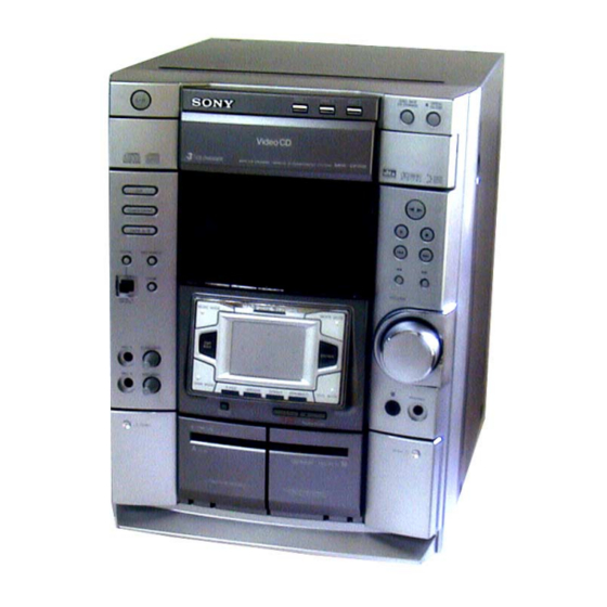
Page 4: General
HCD-VP700 SECTION 1 This section is extracted from instruction manual. GENERAL 3 7 63 1515 0 Parts Identification The items are arranged in alphabetical order. Main unit eaesedefegeh rgrfrdrs L 13942296513 2CH/MULTI rs (27) FM MODE eh (20) BUTTON DESCRIPTIONS CD e;... - Page 5 HCD-VP700 3 7 63 1515 0 Setting the time Turn on the system. Press CLOCK/TIMER SET. When you set the time for the first time, proceed to step 5. Press . or > repeatedly to select “CLOCK SET”. Press ENTER.
-
Page 6: Disassemby
HCD-VP700 SECTION 2 3 7 63 1515 0 DISASSEMBLY • Abbreviation • The equipment can be removed using the following procedure. : Singapre model : Malaysia model Case (Top) Loading Panel Front Panel Section : Thai model Tape Mechanism Deck... - Page 7 HCD-VP700 3 7 63 1515 0 2-2. LOADING PANEL 4 pull-out the disc tray. CD mechanism deck (CDM58) 1 turn the pulley to the direction of arrow. loading panel front panel side pulley 2 pull-out the disc tray. L 13942296513 2-3.
- Page 8 HCD-VP700 3 7 63 1515 0 2-4. TAPE MECHANISM DECK (TCM-230AWR41/MWR41) 1 four screws (+BVTP 2.6 × 8) 2 tape mechanism deck (TCM-230AWR41/MWR41) L 13942296513 2-5. CD PANEL BOARD, PANEL BOARD, OPT IN BOARD 1 five screws (+BVTP 2.6 × 8)
- Page 9 HCD-VP700 3 7 63 1515 0 2-6. ESCUTCHEON PAD (WITH TOUCH PAD) 1 button (edit) 6 two screws (TPG +P 2 × 8) 8 three screws 3 two screws (+BVTP 2.6 × 8) (+BVTP 2.6 × 8) 9 button (DSP) 2 two screws (+BVTP 2.6 ×...
- Page 10 HCD-VP700 3 7 63 1515 0 2-8. TRANS BOARD, MAIN BOARD 8 two screws 4 two screws 6 TRANS board (+BVTP 3 × 8) (+BVTT 4 × 8) 5 two screws 7 two screws (+BVTT 4 × 8) (+BVTT 3 × 8)
- Page 11 HCD-VP700 3 7 63 1515 0 2-10. LEAF SW BOARD, HEAD (A) BOARD, HEAD (B) BOARD (TCM-230AWR41/MWR41) Note: This illustration is for TCM-230MWR, but in case of TCM-230AWR, you can remove them in the same way. 1 five claws 2 LEAF SW board 3 remove the four solderings.
- Page 12 HCD-VP700 3 7 63 1515 0 2-12. BASE UNIT, BD BOARD 1 Pulley(B)(BU-30), chucking 2 Two Screws (+PTPWH M2.6) 3 Lever (lifter) 5 Screw (+PTPWH M2.6) 6 Holder assy 4 Turn the pulley to the direction of arrow. Spring (insulator), coil...
-
Page 13: Test Mode
HCD-VP700 SECTION 3 TEST MODE 3 7 63 1515 0 [Cold Reset] 3. Cursor segment flash on the FL display tube. The input • The cold reset clears all data including preset data stored in the FUNCTION is changed to GAME. - Page 14 HCD-VP700 3 7 63 1515 0 [CD Ship Mode (No Memory Clear)] • This mode moves the position to the position durable to vibra- tion Use this mode when returning the set to the customer after repair. Procedure: 1. Press `/1 button to turn the set ON.
- Page 15 HCD-VP700 3 7 63 1515 0 [VCD COLOR SYSTEM MODE] [VIDEO BOARD] (SIDE A) • This mode is used for changing the COLOR SYSTEM of the VCD. Procedure: 1 2 3 J302 1. Set the standby mode. J301 2-1.Press the two buttons `/1 and > simultaneously to set the COLOR SYSTEM of the VCD to AUTO.
- Page 16 HCD-VP700 3 7 63 1515 0 MEMO L 13942296513 u163 http://www.xiaoyu163.com...
-
Page 17: Mechanical Adjustments
HCD-VP700 SECTION 4 SECTION 5 3 7 63 1515 0 MECHANICAL ADJUSTMENTS ELECTRICAL ADJUSTMENTS Precaution DECK SECTION 0 dB=0.775 V 1. Clean the following parts with a denatured alcohol-moistened swab: 1. Demagnetize the record/playback head with a head record/playback heads pinch rollers demagnetizer. - Page 18 HCD-VP700 3 7 63 1515 0 2. Turn the adjustment screw and check output peaks. If the peaks DECK B Tape Speed Adjustment do not match for L-CH and R-CH, turn the adjustment screw Note: Start the Tape Speed adjustment as below after setting to the test so that outputs match within 1dB of peak.
- Page 19 HCD-VP700 3 7 63 1515 0 DECK B REC Bias Adjustment 4. Mode: Record Procedure: INTRODUCTION MD/VIDEO (AUDIO) IN When set to the test mode performed in Tape Speed Adjustment, 315 Hz, 50 mV (–23.8 dB) AF OSC when the tape is rewound after recording, the “REC memory mode”...
- Page 20 HCD-VP700 3 7 63 1515 0 FM Tuned Level Adjustment CD SECTION Note : FM RF SSG 1. CD Block is basically designed to operate without adjustment. 75 Ω coaxial Therefore, check each item in order given. 2. Use YEDS-18 disc (3-702-101-01) unless otherwise indicated.
- Page 21 HCD-VP700 3 7 63 1515 0 Note: Clear RF signal waveform means that the shape “◊” can be Adjustment Location : clearly distinguished at the center of the waveform. [ BD (CD) BOARD ] — SIDE B — RF signal waveform...
- Page 22 HCD-VP700 3 7 63 1515 0 VIDEO SECTION Frequency Adjustment Connection: frequency counter VIDEO board (27 MHz) Procedure: 1. Connect the frequency counter to check point of the VIDEO board. 2. Turned power switch on. 3. Press the CD button to select the CD.
-
Page 23: Diagrams
HCD-VP700 SECTION 6 DIAGRAMS 3 7 63 1515 0 THIS NOTE IS COMMON FOR PRINTED WIRING BOARDS AND SCHEMATIC DIA- GRAMS. (In addition to this, the necessary note is printed in each block.) Note on Schematic Diagram: Note on Printed Wiring Boards: •... -
Page 24: 6-1. Circuit Board Location
HCD-VP700 3 7 63 1515 0 6-1. CIRCUIT BOARD LOCATION MOTOR board DRIVER board CD SENSOR board BD board VIDEO board HEAD (A) board LEAF SW board HEAD (B) board L 13942296513 SUB TRANS board DSP board TRANS board... -
Page 25: 6-2. Block Diagrams
HCD-VP700 6-2. BLOCK DIAGRAMS 3 7 6 3 1 5 1 5 0 – TUNER/CD SECTION – AM/FM IF MPX IC11 LPF11 • RCH is omitted • Signal Path RF IF L-CH BUFFER ANT IN IF OUT FM IF... - Page 26 HCD-VP700 3 7 6 3 1 5 1 5 0 – MAIN SECTION – IC1220 J601 RV1202 L REC OUT ECHO ECHO IC607(1/2) LEVEV IC1201(1/2) SOUND PROCESSOR R-CH J1201 J1202 MD VIDEO MIC1 MIC2 L IN1 MAC IN TUNER/CD...
- Page 27 HCD-VP700 3 7 6 3 1 5 1 5 0 – VIDEO SECTION – IC501 IC505 (1/2) MPEG VIDEO/AUDIO DEC BUFFER VIDEO SIGNAL PROC IC303 IC304 Y AMP ADATA CD-DATA VIDEO MIX BUFFER TUNER/CD Y OUT L.P.F BCLK CD-BCK...
-
Page 28: Bd Section
HCD-VP700 3 7 6 3 1 5 1 5 0 6-3. SCHEMATIC DIAGRAM – BD SECTION – • See page 53 for Waveforms. • See page 54 for IC Pin Function. • See page 63 for IC Block Diagrams. -
Page 29: Bd Section
HCD-VP700 3 7 6 3 1 5 1 5 0 6-4. PRINTED WIRING BOARD – BD SECTION – • See page 24 for Circuit Boards Location. IC102 CE(DVC) IC104 IC101 XPCK IC103 1 3 9 4 2 2 9 6 5 1 3... -
Page 30: Main Section
HCD-VP700 3 7 6 3 1 5 1 5 0 6-5. PRINTED WIRING BOARD – MAIN SECTION – • See page 24 for Circuit Boards Location. • Semiconductor Location DRIVER VIDEO Ref. No. Location BOARD BOARD BOARD BOARD (Page 47) -
Page 31: Main Section (1/3)
HCD-VP700 3 7 6 3 1 5 1 5 0 6-6. SCHEMATIC DIAGRAM – MAIN (1/3) SECTION – • See page 53 for Waveforms. • See page 63 for IC Block Diagrams. 1 3 9 4 2 2 9 6 5 1 3... -
Page 32: Main Section (2/3)
HCD-VP700 6-7. SCHEMATIC DIAGRAM – MAIN (2/3) SECTION – • See page 53 for Waveforms. • See page 56 for IC Pin Function. 3 7 6 3 1 5 1 5 0 1 3 9 4 2 2 9 6 5 1 3... -
Page 33: Main Section (3/3)
HCD-VP700 3 7 6 3 1 5 1 5 0 6-8. SCHEMATIC DIAGRAM – MAIN (3/3) SECTION – • See page 63, 64 for IC Block Diagrams. 1 3 9 4 2 2 9 6 5 1 3 IC B/D... -
Page 34: Dsp Section
HCD-VP700 6-9. PRINTED WIRING BOARD – DSP SECTION – • See page 24 for Circuit Boards Location. 3 7 6 3 1 5 1 5 0 DSP BOARD (SIDE A) • Semiconductor Location Ref. No. Location D607 D608 D609... -
Page 35: Dsp Section (1/2)
HCD-VP700 3 7 6 3 1 5 1 5 0 6-10. SCHEMATIC DIAGRAM – DSP (1/2) SECTION – • See page 65 for IC Block Diagrams. • See page 59 for IC Pin Function. 1 3 9 4 2 2 9 6 5 1 3... -
Page 36: Dsp Section (2/2)
HCD-VP700 3 7 6 3 1 5 1 5 0 6-11. SCHEMATIC DIAGRAM – DSP (2/2) SECTION – • See page 65 for IC Block Diagrams. – 1 3 9 4 2 2 9 6 5 1 3 IC B/D... -
Page 37: Schematic Diagram
HCD-VP700 3 7 6 3 1 5 1 5 0 6-12. PRINTED WIRING BOARD – OPT SECTION – • See page 24 for Circuit Boards Location. 6-13. SCHEMATIC DIAGRAM – OPT SECTION – OPT IN BOARD 1 3 9 4 2 2 9 6 5 1 3... -
Page 38: Front Amp Section
HCD-VP700 3 7 6 3 1 5 1 5 0 6-14. PRINTED WIRING BOARD – FRONT AMP SECTION – • See page 24 for Circuit Boards Location. MAIN BOARD MAIN BOARD (Page 30) (Page 30) 1 3 9 4 2 2 9 6 5 1 3 •... -
Page 39: Front Amp Section
HCD-VP700 3 7 6 3 1 5 1 5 0 6-15. SCHEMATIC DIAGRAM – FRONT AMP SECTION – 1 3 9 4 2 2 9 6 5 1 3 w w w u 1 6 3 http://www.xiaoyu163.com... -
Page 40: Surround Amp Section
HCD-VP700 3 7 6 3 1 5 1 5 0 6-16. PRINTED WIRING BOARD – SURROUND AMP SECTION – • See page 24 for Circuit Boards Location. (Page 38) (Page 30) D933 R932 R933 (Page 51) 1 3 9 4 2 2 9 6 5 1 3 •... -
Page 41: Surround Amp Section
HCD-VP700 3 7 6 3 1 5 1 5 0 6-17. SCHEMATIC DIAGRAM – SURROUND AMP SECTION – 1 3 9 4 2 2 9 6 5 1 3 w w w u 1 6 3 http://www.xiaoyu163.com... -
Page 42: Panel Section
HCD-VP700 6-18. PRINTED WIRING BOARD – PANEL SECTION – • See page 24 for Circuit Boards Location. 3 7 6 3 1 5 1 5 0 • Semiconductor Location PANEL BOARD Ref. No. Location D1114 D1115 D1116 D1117 Q1114... -
Page 43: Panel Section (1/2)
HCD-VP700 3 7 6 3 1 5 1 5 0 6-19. SCHEMATIC DIAGRAM – PANEL (1/2) SECTION – • See page 53 for Waveforms. • See page 58 for IC Pin Function. 1 3 9 4 2 2 9 6 5 1 3... -
Page 44: Panel Section (2/2)
HCD-VP700 3 7 6 3 1 5 1 5 0 6-20. SCHEMATIC DIAGRAM – PANEL (2/2) SECTION – 1 3 9 4 2 2 9 6 5 1 3 w w w u 1 6 3 http://www.xiaoyu163.com... -
Page 45: Leaf Sw Section
HCD-VP700 3 7 6 3 1 5 1 5 0 6-21. PRINTED WIRING BOARD – LEAF SW SECTION – • See page 24 for Circuit Boards Location. 6-22. SCHEMATIC DIAGRAM – LEAF SW SECTION – 1SS119-25 (Page 30) (Page 31) -
Page 46: Driver Section
HCD-VP700 3 7 6 3 1 5 1 5 0 6-23. PRINTED WIRING BOARD – DRIVER SECTION – • See page 24 for Circuit Boards Location. • Semiconductor Location Ref. No. Location (Page 30) D701 IC701 1 3 9 4 2 2 9 6 5 1 3 IC711 6-24. -
Page 47: Video Section
HCD-VP700 3 7 6 3 1 5 1 5 0 6-25. PRINTED WIRING BOARD – VIDEO SECTION – • See page 24 for Circuit Boards Location. J301 S VIDEO J302 VIDEO C315 C314 R314 R316 C312 L302 L509 Q301... -
Page 48: Video Section (1/3)
HCD-VP700 3 7 6 3 1 5 1 5 0 6-26. SCHEMATIC DIAGRAM – VIDEO (1/3) SECTION – • See page 53 for Waveforms. • See page 61 for IC Pin Function. 1 3 9 4 2 2 9 6 5 1 3... -
Page 49: Video Section (2/3)
HCD-VP700 3 7 6 3 1 5 1 5 0 6-27. SCHEMATIC DIAGRAM – VIDEO (2/3) SECTION – • See page 53 for Waveforms. 1 3 9 4 2 2 9 6 5 1 3 w w w u 1 6 3... -
Page 50: Video Section (3/3)
HCD-VP700 3 7 6 3 1 5 1 5 0 6-28. SCHEMATIC DIAGRAM – VIDEO (3/3) SECTION – • See page 53 for Waveforms. • See page 66 for IC Block Daiagrams. IC B/D 1 3 9 4 2 2 9 6 5 1 3... -
Page 51: Trans Section
HCD-VP700 3 7 6 3 1 5 1 5 0 6-29. PRINTED WIRING BOARD – TRANS SECTION – • See page 24 for Circuit Boards Location. E C B T911 • Semiconductor POWER TRANSFORMER Location Ref. No. Location D911... -
Page 52: Trans Section
HCD-VP700 3 7 6 3 1 5 1 5 0 6-30. SCHEMATIC DIAGRAM – TRANS SECTION – 1 3 9 4 2 2 9 6 5 1 3 w w w u 1 6 3 http://www.xiaoyu163.com... -
Page 53: Tel 13942296513
HCD-VP700 3 7 63 1515 0 • WAVEFORMS – BD BOARD – – MAIN BOARD – IC101 t; (RFAC) IC101 el (FE) IC401 qa (XC-OUT) T301 4 CD PLAY MODE CD PLAY MODE STOP MODE TAPE B REC MODE approx 170mVp-p 80.1kHz... -
Page 54: Ic Pin Function Description
HCD-VP700 3 7 63 1515 0 6-31. IC PIN FUNCTION DESCRINTION • IC101 CXD3068Q (DIGITAL SIGNAL PROCESSOR) (BD Board ) Pin No. Pin Name Discription DVDD0 Digital power supply XRST System reset MUTE Muting selection pin DATA Serial data input, supplied from CPU... - Page 55 HCD-VP700 3 7 63 1515 0 Pin No. Pin Name Discription Tracking error signal input Center servo analog input RFDC RF signal input ADI0 Test pin (Not used) AVSS0 — Analog ground IGEN Power supply pin operational amplifiers AVDD...
- Page 56 HCD-VP700 3 7 63 1515 0 • IC401 MASTER CONTROL (M30622MGA-A36FP) (MAIN Board (2/3)) Pin No. Pin Name Discription AMP - DATA Amp data signal output AMP - CLK Amp clock signal output AMP - LAT Amp latch signal output...
- Page 57 HCD-VP700 3 7 63 1515 0 Discription Pin No. Pin Name NO - USE Not used B TRG B deck trigger control signal output AMS - IN AMS signal input CAPM - H/L Capstan moter highi/low speed control signal output...
- Page 58 HCD-VP700 3 7 63 1515 0 • IC1101 DISPLAY CONTROL (MB90M407APF-G-105-BND) (PANEL Board (1/2)) Discription Pin No. Pin Name FIPLED16 Grid drive signal output to the fluorescent indicator 2 - 5 FIP17 - 20 Grid drive signal output to the fluorescent indicator...
- Page 59 HCD-VP700 3 7 63 1515 0 • IC601 DECODER (CXD9617R) (DSP Board (1/2)) Pin No. Pin Name Discription — Ground XRST Reset signal input EXTIN Not used (connected to ground) Not used (connected to ground) VDDI Power supply Not used (connected to ground)
- Page 60 HCD-VP700 3 7 63 1515 0 Pin No. Pin Name Discription MOD0 Operation mode signal input (L : single chip mode, H : use prohibited) EXLOCK Lock signal input VDDI Power supply — Ground 62, 63 A17, A16 Not used (open)
- Page 61 HCD-VP700 3 7 63 1515 0 • IC502 M30622MGA-A59FP (CD MECHANISM CONTROLLER) (VIDEO BOARD) Discription Pin No. Pin Name SENSE Internal state (SENSE) monitor input SENSE CLK Serial data reading clock output RESOLUTION Y resolution output CROMA LEVEL Chroma level controll signal output...
- Page 62 HCD-VP700 3 7 63 1515 0 Pin No. Pin Name Discription INSW Not used (connected to +5V) OUTSW Not used (open) MODEL 1 Not used (open) MODEL 2 Not used (open) TBLL Not used (open) TBLR Not used (open)
-
Page 63: Ic Block Diagrams
HCD-VP700 3 7 63 1515 0 6-32. IC BLOCK DIAGRAMS IC103 CXA2581N-T4 (BD BOARD) OFST RW/ROM RFDCI DVCC 11 RFDCO EQ IN 26 RFC 25 VFC 24 BST AC SUM ON/OFF 23 RFG VOFST 22 VCC RW/ROM VOFST RW/ROM... - Page 64 HCD-VP700 3 7 63 1515 0 IC51 LC72131D (MAIN BOARD (3/3)) PHASE DETECTOR CHARGE PUMP POWER REFERENCE UNLOCK DIVIDER DETECTOR RESET SWALLOW COUNTER 1/16, 1/17 4BITS 12BITS PROGRAMMABLE DRIVER UNIVERSAL DATA SHIFT REGISTER LATCH INTERFACE COUNTER 2 3 4 5...
- Page 65 HCD-VP700 3 7 63 1515 0 IC605 AK4527 (DSP BOARD (1/2)) 44 43 42 41 40 39 38 37 36 35 34 AUDIO MCLK DZF2 RIN+ SDOS SDOUT RIN– LIN– FORMAT LIN+ CONVERTER SMUTE DATT ROUT1 BICK BICK LRCK...
- Page 66 HCD-VP700 3 7 63 1515 0 IC302 NJM2255M (VIDEO BOARD) IC303 NJM2209M (VIDEO BOARD) SATURATION +Ø ADJUST (COLOR BURST) HUE ADJUST SATURATION SECONDARY LOWER CLAMP ADJUST DIFFERENTIATION LIMITER SYNC –X (COLOR BURST) GAIN ADJ CHIP SWITCH CONTROL LOWER LIMITER...
-
Page 67: Exploded Views
HCD-VP700 SECTION 7 EXPLODED VIEWS 3 7 63 1515 0 NOTE: • -XX, -X mean standardized parts, so they may • Hardware (# mark) list and accessories and The components identified by have some differences from the original one. -
Page 68: 7-2. Front Panel Section
HCD-VP700 3 7 63 1515 0 7-2. FRONT PANEL SECTION Tape mechanism deck FL1101 not supplied not supplied L 13942296513 Supplied with S1101 Ref. No. Part No. Description Remarks Ref. No. Part No. Description Remarks 4-231-804-01 KNOB (VOL) 4-231-836-01 SPRING (HEART CAM-A) -
Page 69: 7-3. Chassis Section
HCD-VP700 3 7 63 1515 0 7-3. CHASSIS SECTION not supplied not supplied not supplied (MY, SP) T911 not supplied (TH) L 13942296513 not supplied The components identified by mark 0 or dotted line with mark 0 are critical for safety. -
Page 70: Tape Mechanism Deck Section-1 (Tcm-230Mwr41)
HCD-VP700 3 7 63 1515 0 7-4. TAPE MECHANISM DECK SECTION-1 (TCM-230MWR41) • The thing that a part A curves is TCM-230MWR41. Note: Two different types of tape mechanism are used depending on models. They maintain compatibility as an entire mechanism even though there are some different parts are used. -
Page 71: Tape Mechanism Deck Section-2 (Tcm-230Awr41)
HCD-VP700 3 7 63 1515 0 7-5. TAPE MECHANISM DECK SECTION-2 (TCM-230AWR41) • The thing that a part A doesn’t curve is TCM-230AWR41. Note: Two different types of tape mechanism are used depending on models. They maintain compatibility as an entire mechanism even though there are some different parts are used. -
Page 72: Cd Mechanism Deck Section (Cdm58E-30Bd61A)
HCD-VP700 3 7 63 1515 0 7-6. CD MECHANISM DECK SECTION (CDM58E-30BD61A) M721 not supplied L 13942296513 BU-30BD61 Ref. No. Part No. Description Remarks Ref. No. Part No. Description Remarks X-4953-306-1 HOLDER (BU) (BU-30) ASSY 4-933-134-11 SCREW (+PTPWH M2.6X8) -
Page 73: Base Unit Section (Bu-30Bd61A)
HCD-VP700 3 7 63 1515 0 7-7. BASE UNIT SECTION (BU-30BD61A) L 13942296513 Ref. No. Part No. Description Remark Ref. No. Part No. Description Remark 1-782-817-11 WIRE (FLAT TYPE) (16 CORE) A-4725-561-A BD BOARD, COMPLETE A-4735-189-A BU-30 (61) ASSY u163 http://www.xiaoyu163.com... -
Page 74: Electrical Parts List
HCD-VP700 SECTION 8 ELECTRICAL PARTS LIST 3 7 63 1515 0 Ref. No. NOTE: Part No. Description Remarks Ref. No. Part No. Description Remarks • Due to standardization, replacements in the • COILS uH: µH parts list may be different from the parts... - Page 75 HCD-VP700 CD PANEL CD SENSOR DRIVER 3 7 63 1515 0 Ref. No. Part No. Description Remarks Ref. No. Part No. Description Remarks R167 1-216-864-11 METAL CHIP 1/16W R1151 1-249-422-11 CARBON 2.7K 1/4W F R168 1-216-864-11 METAL CHIP 1/16W...
-
Page 76: Q Q
HCD-VP700 3 7 63 1515 0 Ref. No. Part No. Description Remarks Ref. No. Part No. Description Remarks C603 1-164-156-11 CERAMIC CHIP 0.1uF C678 1-126-964-11 ELECT 10uF C604 1-164-156-11 CERAMIC CHIP 0.1uF C679 1-164-156-11 CERAMIC CHIP 0.1uF C605 1-164-156-11 CERAMIC CHIP 0.1uF... - Page 77 HCD-VP700 3 7 63 1515 0 Ref. No. Part No. Description Remarks Ref. No. Part No. Description Remarks < DIODE > R602 1-216-813-11 METAL CHIP 1/16W R603 1-216-809-11 METAL CHIP 1/16W D601 8-719-158-02 DIODE RD3.9SB2 R604 1-216-809-11 METAL CHIP...
- Page 78 HCD-VP700 FRONT AMP 3 7 63 1515 0 Ref. No. Part No. Description Remarks Ref. No. Part No. Description Remarks R685 1-216-809-11 METAL CHIP 1/16W R768 1-216-833-11 METAL CHIP 1/16W R686 1-216-809-11 METAL CHIP 1/16W R769 1-216-821-11 METAL CHIP...
- Page 79 HCD-VP700 FRONT AMP 3 7 63 1515 0 Ref. No. Part No. Description Remarks Ref. No. Part No. Description Remarks C886 1-162-306-11 CERAMIC 0.01uF R810 1-260-076-11 CARBON 1/2W 0 R811 C923 1-126-964-11 ELECT 10uF 1-212-881-11 FUSIBLE 1/4W C924 1-126-926-11 ELECT...
-
Page 80: Ao Y U163
HCD-VP700 MAIN FRONT AMP HEAD (A) HEAD (B) LEAF SW 3 7 63 1515 0 Ref. No. Part No. Description Remarks Ref. No. Part No. Description Remarks ****************************************************** < TERMINAL > TM801 1-694-677-12 TERMINAL BOARD (4P) (FRONT SPEAKER) A-4475-698-A MAIN BOARD, COMPLETE (SP,MY) - Page 81 HCD-VP700 MAIN 3 7 63 1515 0 Ref. No. Part No. Description Remarks Ref. No. Part No. Description Remarks C141 1-126-964-11 ELECT 10uF C357 1-126-960-11 ELECT C143 1-126-964-11 ELECT 10uF C358 1-126-964-11 ELECT 10uF C155 1-126-964-11 ELECT 10uF C359 1-137-194-11 FILM 0.47uF...
- Page 82 HCD-VP700 MAIN 3 7 63 1515 0 Ref. No. Part No. Description Remarks Ref. No. Part No. Description Remarks < CONNECTOR > IC301 8-759-652-02 IC HA12226F IC302 8-759-143-54 IC uPC1330HA CN101 1-774-876-21 CONNECTOR, BOARD TO BOARD 8P IC303 8-759-656-83 IC NJM4580MD-(TE2)
- Page 83 HCD-VP700 MAIN 3 7 63 1515 0 Ref. No. Part No. Description Remarks Ref. No. Part No. Description Remarks < TRANSISTOR > 1-216-864-11 METAL CHIP 1/16W 1-216-833-11 METAL CHIP 1/16W 8-729-055-80 TRANSISTOR 2SC1674LK-TP 1-216-845-11 METAL CHIP 100K 1/16W 8-729-422-57 TRANSISTOR UN4111...
- Page 84 HCD-VP700 MAIN 3 7 63 1515 0 Ref. No. Part No. Description Remarks Ref. No. Part No. Description Remarks R336 1-216-846-11 METAL CHIP 120K 1/16W R402 1-216-809-11 METAL CHIP 1/16W R337 1-216-813-11 METAL CHIP 1/16W R403 1-216-809-11 METAL CHIP...
- Page 85 HCD-VP700 MAIN MOTOR OPT IN OPT IN REAR PANEL 3 7 63 1515 0 Ref. No. Part No. Description Remarks Ref. No. Part No. Description Remarks *********** R504 1-216-841-11 METAL CHIP 1/16W R505 1-216-833-11 METAL CHIP 1/16W R506 1-216-827-11 METAL CHIP 3.3K...
- Page 86 HCD-VP700 PANEL 3 7 63 1515 0 Ref. No. Part No. Description Remarks Ref. No. Part No. Description Remarks C1130 1-162-282-31 CERAMIC 100PF D1110 8-719-050-84 DIODE RB441Q-40T-77 C1131 1-162-282-31 CERAMIC 100PF D1111 8-719-057-97 DIODE SEL5923A-TP15 (EFFECT) C1132 1-162-282-31 CERAMIC...
- Page 87 HCD-VP700 PANEL 3 7 63 1515 0 Ref. No. Part No. Description Remarks Ref. No. Part No. Description Remarks R1117 1-247-807-31 CARBON 1/4W R1190 1-249-441-11 CARBON 100K 1/4W R1118 1-247-807-31 CARBON 1/4W R1191 1-260-083-11 CARBON 1/2W R1119 1-249-417-11 CARBON...
- Page 88 HCD-VP700 SUB TRANS SURROUND AMP PANEL 3 7 63 1515 0 Ref. No. Part No. Description Remarks Ref. No. Part No. Description Remarks S1121 1-762-875-21 SWITCH, KEYBOARD (M ) S1122 1-762-875-21 SWITCH, KEYBOARD (m ) < IC > S1123...
- Page 89 HCD-VP700 SURROUND AMP TRANS VIDEO 3 7 63 1515 0 Ref. No. Part No. Description Remarks Ref. No. Part No. Description Remarks R933 1-249-422-11 CARBON 2.7K 1/4W F C308 1-162-959-11 CERAMIC CHIP 330PF R934 1-249-429-11 CARBON 1/4W C309 1-162-959-11 CERAMIC CHIP...
- Page 90 HCD-VP700 VIDEO 3 7 63 1515 0 Ref. No. Part No. Description Remarks Ref. No. Part No. Description Remarks C569 1-126-206-11 ELECT CHIP 100uF 6.3V < TRANSISTOR > C570 1-126-206-11 ELECT CHIP 100uF 6.3V Q301 8-729-900-53 TRANSISTOR DTC114EKA-T146 C571...
- Page 91 HCD-VP700 VIDEO 3 7 63 1515 0 Ref. No. Part No. Description Remarks Ref. No. Part No. Description Remarks R537 1-216-809-11 METAL CHIP 1/16W 7-685-872-09 SCREW +BVTT 3X8 (S) R538 1-216-833-11 METAL CHIP 1/16W 7-623-921-01 RING, RETAINING, CAPSTAN 7-628-254-05 SCREW +PS 2.6X5...
- Page 92 HCD-VP700 3 7 63 1515 0 REVISION HISTORY Clicking the version allows you to jump to the revised page. Also, clicking the version at the upper right on the revised page allows you to jump to the next revised page.