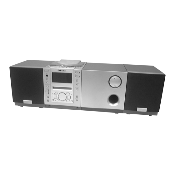
Sony PMC-MD55 Service Manual
Personal minidisc system
Hide thumbs
Also See for PMC-MD55:
- Operating instructions manual (164 pages) ,
- Operating instructions manual (76 pages) ,
- Service manual (220 pages)
Table of Contents
Quick Links
See also:
Service Manual
SERVICE MANUAL
Ver 1.1 1999. 08
U.S. and foreign patents licensed form Dolby Laboratories
Licensing Corporation.
MW: 531 - 1,602 kHz (AEP, UK)
LW: 153 - 279 kHz (AEP, UK)
MICROFILM
SPECIFICATIONS
(US only)
(US, Canadian)
87.5 - 108 MHz (AEP, UK)
(US, Canadian)
PMC-MD55
Model Name Using Similar Mechanism
CD
CD Mechanism Type
Section
Optical Pick-up Name
Model Name Using Similar Mechanism
MD
MD Mechanism Type
Section
Base Unit Name
Optical Pick-up Name
AM (MW/LW): Loop antenna
PERSONAL MINIDISC SYSTEM
US Model
Canadian Model
AEP Model
UK Model
NEW
KSM-213CGP
KSS-213C
MDS-JB920
MDM-5A
MBU-5A
KMS-260A
– Continued on next page –
Table of Contents

Related Manuals for Sony PMC-MD55


Summary of Contents for Sony PMC-MD55
- Page 1 PMC-MD55 SERVICE MANUAL US Model Canadian Model Ver 1.1 1999. 08 AEP Model UK Model Model Name Using Similar Mechanism U.S. and foreign patents licensed form Dolby Laboratories Licensing Corporation. CD Mechanism Type KSM-213CGP Section Optical Pick-up Name KSS-213C Model Name Using Similar Mechanism...
-
Page 2: Table Of Contents
DES PIÈCES SONT CRITIQUES POUR LA SÉCURITÉ DE FONCTIONNEMENT. NE REMPLACER CES COM- ELECTRICAL PARTS LIST ......128 POSANTS QUE PAR DES PIÈCES SONY DONT LES NUMÉROS SONT DONNÉS DANS CE MANUEL OU DANS LES SUPPLÉMENTS PUBLIÉS PAR SONY. – 2 –... -
Page 3: Servicing Notes
SECTION 1 SERVICING NOTES SAFETY CHECK-OUT CAUTION After correcting the original service problem, perform the follow- Use of controls or adjustments or performance of procedures ing safety check before releasing the set to the customer: other than those specified herein may result in hazardous ra- Check the antenna terminals, metal trim, “metallized”... - Page 4 JIG FOR CHECKING BD BOARD WAVEFORM The special jig (J-2501-149-A) is useful for checking the waveform of the BD board. The names of terminals and the checking items to be performed are shown as follows. GND : Ground I+3V : For measuring IOP (Check the deterioration of the optical pick-up laser) IOP : For measuring IOP (Check the deterioration of the optical pick-up laser) TEO : TRK error signal (Traverse adjustment) VC : Reference level for checking the signal...
- Page 5 CHECKS PRIOR TO PARTS REPLACEMENT AND ADJUSTMENTS (for MD Section) Before performing repairs, perform the following checks to determine the faulty locations up to a certain extent. Details of the procedures are described in “5 Electrical Adjustments”. Criteria for Determination Measure if unsatisfactory: (Unsatisfactory if specified value is not satisfied) Laser power check...
-
Page 6: General
SECTION 2 This section is extracted from instruction manual. GENERAL – 6 –... - Page 7 – 7 –...
- Page 8 – 8 –...
-
Page 9: Disassembly
SECTION 3 DISASSEMBLY • This set can be disassembled in the order shown below. Rear cabinet Front cabinet block Upper cabinet block CD PICK-UP assy Main board section Main board TU block, MD block MD mechanism deck Slider (CAM) Base unit (MBU-5A), BD board SW board, loading motor (M103) Note: Follow the disassembly procedure in the numerical order given. - Page 10 FRONT CABINET BLOCK 1 three screws (BVTP3 × 12) 2 harness 1 three screws (BVTP3 × 12) 3 wire, parallel (ffc) 12P (CN407) 4 cabinet (front) block UPPER CABINET BLOCK 4 cabinet (upper) block 2 connector (CN711) 1 wire, parallel (ffc) 16P (from OPTICAL PICK-UP connector) 1 wire, parallel (ffc) 11P (CN1001)
- Page 11 CD PICK-UP ASSY 2 PICK-UP assy 1 two screws (PWH2.6 × 10) 1 two screws (PWH2.6 × 10) MAIN BOARD SECTION 1 connector 2 wire parallel (ffc) 16P 1 connector 3 two screws (CN302) (CN701) (CN704) (BVTP3 × 10) 1 connector (CN303) 3 two screws (BVTP3 ×...
- Page 12 MAIN BOARD shield plate (main) 1 two screws (BVTT2.6 × 6) 1 two screws (BVTT2.6 × 6) 2 main board TU BLOCK, MD BLOCK 6 two screws (BVTP3 × 10) 7 TU block assy 8 two screws (BVTP3 × 10) 8 screw 0 MD block assy (BVTP3 ×...
- Page 13 MD MECHANISM DECK 2 shield plate (upper) 1 four claws 5 two screws 5 two screws (BVTTWH M3) (BVTTWH M3) 3 connector (CN601) 7 MD mechanism deck (MDM-5A) 4 wire, parallel (ffc) 21P (CN102) 4 wire, parallel (ffc) 23P (CN103) 6 harness SLIDER (CAM) 6 slider (Cam)
- Page 14 BASE UNIT (MBU-5A), BD BOARD 2 base unit (MBU-5A) 5 flexible board (CN104) 6 flexible board (CN101) 1 three screws (P2.6 × 6) 3 Remove the solder (Five portion). 7 BD board 4 screw (M1.7 × 4) SW BOARD, LOADING MOTOR (M103) 1 screw (PTPWH M2.6 ×...
-
Page 15: Test Mode
SECTION 4 TEST MODE Refer to “5. ELECTRICAL ADJUSTMENT” for the test mode of CD section. MD SECTION 1. PRECAUTIONS FOR USE OF TEST MODE • As loading related operations will be performed regardless of the test mode operations being performed, be sure to check that the disc is stopped before setting and removing it. - Page 16 5. SELECTING THE TEST MODE There are 9 types of test modes as shown below. The mode can be switched by turning the JOG dial. After selecting the mode to be used, [YES, ENTER] press the button. Display Contents TEMP ADJUST Temperature compensation offset adjustment LDPWR ADJUST Laser power adjustment...
- Page 17 5-1. Operating the Continuous Playback Mode 1. Entering the continuous playback mode (1) Set the disc in the unit. (Whichever recordable discs or discs for playback only are available) (2) Turn the JOG dial and display “CPLAY MODE”. [YES, ENTER] (3) Press the button to change the display to “CPLAY MID”.
- Page 18 6. FUNCTIONS OF OTHER BUTTONS Function Contents Sets continuous playback when pressed in the STOP state. When pressed during continuous playback, 7, MD and EDIT the tracking servo turns ON/OFF. s (MD) and EDIT Stops continuous playback and continuous recording. The sled moves to the outer circumference only when this is pressed.
-
Page 19: Electrical Adjustments
SECTION 5 ELECTRICAL ADJUSTMENTS AM IF ADJUSTMENT TUNER SECTION 0 dB=1 µV Adjust for a maximum reading on level meter [AM (MW/LW)] 450 kHz Setting: Function : RADIO AM VT VOLTAGE CONFIRMATION (US, Canadian) BAND switch: AM (MW/LW) Frequency Display Reading on Digital Voltmeter Put the lead-wire + 0.8... - Page 20 Adjustment Location: – TU BOARD (Component Side) – FM tracking Adjustment (US, Canadian) MW Tracking Adjustment (AEP, UK) FM VT Voltage Adjustment (US, Canadian) LW Tracking Adjustment (AEP, UK) AM IF Adjustment CT5 LW VT Voltage Adjustment (AEP, UK) MW VT Voltage Adjustment AM Tracking Adjustment (AEP, UK) (US, Canadian)
-
Page 21: Md Section
MD SECTION 1. PARTS REPLACEMENT AND ADJUSTMENT • Check and adjust the mechanism deck as follows. The procedure changes according to the part replaced. • Abbreviation : Optical pick-up OWH : Overwrite head • Laser power check • Focus bias check •... - Page 22 2. PRECAUTIONS FOR CHECKING LASER DIODE 4. Use the following tools and measuring devices. • Check Disc (MD) TDYS-1 EMISSION (Part No. 4-963-646-01) To check the emission of the laser diode during adjustments, never • Test Disc (MDW-74/AU-1) (Part No. 8-892-341-41) view directly from the top as this may lose your eye-sight.
- Page 23 6. CHECK PRIOR TO REPAIRS 6-2. Focus Bias Check Change the focus bias and check the focus tolerance amount. These checks are performed before replacing parts according to Checking Procedure : “approximate specifications” to determine the faulty locations. For 1. Load the test disk (MDW-74/AU-1). details, refer to “Checks Prior to Parts Replacement and Adjust- 2.
-
Page 24: Laser Power Adjustment
7. TEMPERATURE COMPENSATION OFFSET 7. Then, turn the JOG dial to display “LDPWR CHECK”. [YES, ENTER] 8. Press the button once to display “LD 0.9 mW ADJUSTMENT ”. Check that the reading of the laser power meter become Save the temperature data at that time in the non-volatile memory 0.85 to 0.91 mW. - Page 25 9. EF BALANCE ADJUSTMENT 8. Turn the JOG dial so that the waveform of the oscilloscope becomes the specified value. (When the JOG dial is turned, the of “EFB- ” changes Note 1:Data will be erased during MO reading if a recorded disc is used in this adjustment.
- Page 26 [YES, ENTER] 11. ERROR RATE CHECK 17. Press the button, display “EFB = SAVE” for a moment and save the adjustment results in the non-vola- tile memory. 11-1. CD Error Rate Check Next “EFBAL ADJUST” will be displayed. Checking Procedure : [MD EJECT 18.
- Page 27 Adjustment Location: – BD BOARD (Component Side) – CN101 D101 CN110 I+3V NOTE IC171 – BD BOARD (Conductor Side) – IC101 IC121 IC192 Note: It is useful to use the jig for checking the waveform. (Refer to Ser- vicing Notes on page 4) –...
-
Page 28: Cd Section
Display CD SECTION Set the CD test mode when performing confirmations. After completing the confirmation, release the CD test mode. XX XXX In the CD test mode, the set works as following sequence. CD test mode sequence: 1. Enter the CD test mode 2. - Page 29 4. ALL SERVO ON Mode 1 6. Releasing the CD Test Mode (RF Level and Jitter Confirmation 1) 1. Press the (CD) button to stop rotate the disc. [POWER] [RESET] 2. Press the button or switch (bottom of the 1. Press the button four times to enter the ALL SERVO player unit) to release the CD test mode and turn to standby ON mode 1 (start playback the disc) and display as below.
-
Page 30: Display Section
DISPLAY SECITON Dimmer Adjustment Connection: digital voltmeter LCD board TP (DIMMER) TP (GND) – 1. Connect a digital voltmeter to TP (DIMMER) and TP (GND) on the LCD board. 2. Adjust RV550 so that the value of digital voltmeter becomes 2.83 V. -
Page 31: Diagrams
PMC-MD55 SECTION 6 DIAGRAMS 6-1. BLOCK DIAGRAM – TUNER Section – TU BOARD (AEP, UK) FM TUNER UNIT FM EXT IF OUT ANTENNA 10.7MHz IF, DET, FM MPX (AEP, UK) OSC OUT IC1 (2/2) FM/AM FRONT-END (US, CND) IC1 (1/2) -
Page 32: Block Diagram - Md Section
PMC-MD55 6-2. BLOCK DIAGRAM – MD Section – CN102 CN601 BD BOARD (1/2) DG BOARD CN603 LEVEL FROM CD D-IN DIGITAL SIGNAL PROCESSOR, SHIFT SECTION EFM/ACIRC ENCODER/DECODER, IC604 (Page 39) D/A, A/D +3.3V SHOCK PROOF MEMORY CONTROLLER, MD B+ CONVERTER ATRAC ENCODER/DECODER (+3.3V) -
Page 33: Block Diagram - Cd Section
PMC-MD55 6-3. BLOCK DIAGRAM – CD Section – MAIN BOARD (3/6) CN704 TO MD DOUT D-OUT OPTICAL PICK-UP SECTION RF AMP, FOCUS/TRACKING SERVO BLOCK DIGITAL SIGNAL PROCESSOR, (Page 36) IC701 CLV SERVO, D/A CONVERTER (KSS-213C) CN701 IC702 TO FUNCTION RF AMP... -
Page 34: Block Diagram - Function Select/Panel Section
PMC-MD55 6-4. BLOCK DIAGRAM – FUNCTION SELECT/PANEL Section – MAIN BOARD (4/6) CN405 TUNER/LINE IN (1/2) SELECT TO MD AD-LCH IC301 SECTION CN408 (Page 36) (2/2) RADIO FROM TUNER RA-LCH AU/JACK BOARD (1/4) SECTION (Page 33) CN302 CN307 (1/3) 0dB/6dB... -
Page 35: Block Diagram - Power Amp/Power Supply Section
PMC-MD55 6-5. BLOCK DIAGRAM – POWER AMP/POWER SUPPLY Section – J301 POWER AMP (A) POWER AMP (C) BOARD AU/JACK BOARD (3/4) SIGNAL OUTPUT LINE BOARD (TO SPEAKER(L) UNIT) CN392 IC352 +OUT2 CN393 CN394 FROM FUNCTION POWER SP391 SELECT SECTION L-CH (Page 42) –OUT2... -
Page 36: Block Diagram - Super Woofer Section
PMC-MD55 6-6. BLOCK DIAGRAM – SUPER WOOFER Section – WOOFER AMP (B) BOARD W-VOLUME WOOFER AMP (A) BOARD J811 WOOFER BOARD SIGNAL INPUT FILTER AMP (WOOFER) IC811 CN803 CN803 CN821 CN821 IC812 (2/2) (1/2) (TO PLAYER UNIT) (1/2) (2/2) CN812... - Page 37 • Circuit Bords Location – Player Unit – SW board CD O/C board SW (TOP) board CD MOTOR board LAMP board AU/JACK board TU board SW (FRONT) board LCD board MAIN board BD board DG board LINE IN board – Speaker (L) Section – POWER board POWER AMP (C) board POWER AMP (A) board...
- Page 38 – Super Woofer Section – W-POWER board WOOFER AMP (A) board WOOFER AMP (B) board W-LED board W-VOLUME board – 48 –...
-
Page 40: Schematic Diagram - Tuner Section
6-8. SCHEMATIC DIAGRAM – TUNER Section – • See page 99 for Waveforms. • See page 101 for IC Block Diagrams. PMC-MD55 (Page 70) (Page 70) – 51 – – 52 –... -
Page 41: Schematic Diagram - Bd Section
PMC-MD55 6-9. SCHEMATIC DIAGRAM – BD Section – • See page 99 for Waveforms. • See page 102 for IC Block Diagrams. (Page 54) (Page 61) (Page 61) Note on Schematic Diagram: • All capacitors are in µF unless otherwise noted. pF: µµF •... -
Page 44: Schematic Diagram - Dg Section
PMC-MD55 6-12. SCHEMATIC DIAGRAM – DG Section – • See page 99 for Waveforms. • See page 104 for IC Block Diagrams. (Page 55) (Page 55) (Page 70) (Page 55) (Page 67) Note on Schematic Diagram: • All capacitors are in µF unless otherwise noted. pF: µµF •... -
Page 46: Schematic Diagram - Main (Cd) Section
PMC-MD55 6-14. SCHEMATIC DIAGRAM – MAIN (CD) Section – • See page 100 for Waveforms. • See page 105 for IC Block Diagrams. (Page 70) (Page 73) (Page 79) Note on Schematic Diagram: • All capacitors are in µF unless otherwise noted. pF: µµF 50 WV or less are not indicated except for electrolytics and tantalums. -
Page 47: Main (System Control) Section
PMC-MD55 6-15. SCHEMATIC DIAGRAM – MAIN (SYSTEM CONTROL) Section – • • See page 100 for Waveforms. See page 104 for IC Block Diagram. (Page 73) (Page 73) (Page 69) (Page (Page (Page 78) (Page 73) (Page 89) (Page (Page 78) -
Page 48: Schematic Diagram - Main (Function Select) Section
PMC-MD55 6-16. SCHEMATIC DIAGRAM – MAIN (FUNCTION SELECT) Section – (Page 69) (Page 70) (Page 77) (Page 77) (Page 72) (Page 70) Note on Schematic Diagram: • All capacitors are in µF unless otherwise noted. pF: µµF • Voltages are taken with a VOM 50 WV or less are not indicated except for electrolytics (Input impedance 10 MΩ). -
Page 50: Schematic Diagram - Audio/Jack Section
PMC-MD55 6-18. SCHEMATIC DIAGRAM – AUDIO/JACK Section – • See page 107 for IC Block Diagram. (Page 93) (Page 97) (Page 72) (Page 93) (Page 72) (Page 74) (Page 74) Note on Schematic Diagram: • All capacitors are in µF unless otherwise noted. pF: µµF... -
Page 51: Schematic Diagram - Cd Motor Section
PMC-MD55 6-19. SCHEMATIC DIAGRAM – CD MOTOR Section – • See page 107 for IC Block Diagram. (Page 67) Note on Schematic Diagram: • All capacitors are in µF unless otherwise noted. pF: µµF 50 WV or less are not indicated except for electrolytics and tantalums. -
Page 54: Schematic Diagram - Cd Open/Close Section
PMC-MD55 6-22. SCHEMATIC DIAGRAM – CD OPEN/CLOSE Section – • See page 107 for IC Block Diagram. (Page 72) Note on Schematic Diagram: • All capacitors are in µF unless otherwise noted. pF: µµF 50 WV or less are not indicated except for electrolytics and tantalums. -
Page 56: Schematic Diagram - Panel Section
PMC-MD55 6-24. SCHEMATIC DIAGRAM – PANEL Section – (Page 72) (Page 72) (Page 72) Note on Schematic Diagram: • All capacitors are in µF unless otherwise noted. pF: µµF 50 WV or less are not indicated except for electrolytics and tantalums. -
Page 58: Schematic Diagram - Power Amp/Power Section
PMC-MD55 6-26. SCHEMATIC DIAGRAM – POWER AMP/POWER Section – (Page 78) Note on Schematic Diagram: • All capacitors are in µF unless otherwise noted. pF: µµF 50 WV or less are not indicated except for electrolytics and tantalums. • All resistors are in Ω and W or less unless otherwise specified. - Page 60 PMC-MD55 6-28. SCHEMATIC DIAGRAM – SUPER WOOFER Section – • See page 107 for IC Block Diagram. (Page 78) Note on Schematic Diagram: • All capacitors are in µF unless otherwise noted. pF: µµF 50 WV or less are not indicated except for electrolytics and tantalums.
- Page 61 • Waveforms – TU BOARD – – DG BOARD – – MAIN BOARD 4 IC121 !§ (OSCI) 6 IC605 6 5 IC702 $£ (BCK) (CD Play Mode) 1 IC1 0 (QUAD) 1 IC601 @• (XIN) (SYSTEM CONTROL Section) – 1 V/DIV, 10 ns/DIV 200 mV/DIV, 10 ns/DIV 1 V/DIV, 200 ns/DIV 50 mV/DIV, 50 ns/DIV...
-
Page 62: Ic Block Diagrams
• IC Block Diagrams – TU Board – IC1 TA2104AN GND1 FM RF OUT FM RF VCC1 FM RF IN AM RF IN AM LOW OUT MIX OUT FM OSC AM OSC BUFF VCC2 BUFF OSC OUT LEVEL AM IF AM IF IN ST IND IF BUFF... - Page 63 – BD Board – IC101 CXA2523AR 43 42 USROP – RF AGC – USRC RFA1 BPF3T RFA2 PEAK3T – HLPT –1 – – –2 – CFST PTGR TEMP PEAK – –2 – BOTTOM 36 BOTM – –1 GRVA 35 ABCD 34 FE 33 AUX –...
- Page 64 IC121 CXD2654R 100 99 98 97 96 95 94 93 92 91 90 89 88 87 86 85 84 83 82 81 80 79 78 77 76 SPINDLE GENERATOR SERVO 75 TE MNT0 74 SE MNT1 EACH MONITOR 73 AVSS BLOCK CONTROL MNT2...
-
Page 65: Main Board
– DG Board – IC603 PCM3003E/T2 A/D CONVERTER D/A CONVERTER VCC2 BLOCK BLOCK VCC1 AGND1 AGND2 VCC1 ANALOG ANALOG ANALOG ANALOG VCOM VINR FRONT-END FRONT-END LOW-PASS LOW-PASS VOUTR CIRCUIT CIRCUIT FILTER FILTER VOUTL VREF1 REFERENCE VREF2 MULTI-LEVEL MULTI-LEVEL VINL ∆Σ ∆Σ... - Page 66 IC701 CXA2542AQ PD1 IV SUMMING PD2 37 SENS2 PD2 IV LASER POWER CONTROL ↓ SENS1 F IV AMP FE AMP C. OUT E IV AMP LEVEL S FO. BIAS XRST WINDOW COMP. ↓ MIRR TRK. GAIN DATA WINDOW COMP. ↓ E-F BALANCE WINDOW COMP.
- Page 67 IC702 CXD3009Q 59 58 57 56 55 54 46 45 44 DIGITAL DEMODULATOR SERIAL-IN INTERFACE 40 LRCKI VDD3 SYSM D / A ERROR D / A INTERFACE INTERFACE CORRECTOR 39 LRCK AVSS 38 ASYO AVDD 37 ASYI ASYMMETRY CORRECTOR AOUT1 36 BIAS 16K RAM 35 RF...
- Page 68 – AU/JACK Board – IC351 BH3863F-E2 19 18 17 16 15 14 DIGITAL DINAMIC DINAMIC FILTER FILTER CONTROL BASS BASS TREBLE TREBLE 0dB/6dB 0dB/6dB BASS BASS 10 11 12 – CD MOTOR Board – IC1001 BA6892FP-E2 28 27 23 22 21 20 19 18 17 16 15 PVCC MUTING...
- Page 69 6-29. IC PIN FUNCTION DESCRIPTION • BD BOARD IC101 CXA2523AR (RF AMP, FOCUS/TRACKING ERROR AMP) Pin No. Pin Name Description I-V converted RF signal I input from the optical pick-up block detector I-V converted RF signal J input from the optical pick-up block detector Middle point voltage (+1.65V) generation output terminal 4 to 9 A to F...
- Page 70 • BD BOARD IC121 CXD2654R (DIGITAL SIGNAL PROCESSOR, DIGITAL SERVO SIGNAL PROCESSOR, EFM/ACIRC ENCODER/DECODER, SHOCK PROOF MEMORY CONTROLLER, ATRAC ENCODER/DECODER) Pin No. Pin Name Description Focus OK signal output to the MD mechanism controller (IC601) MNT0 (FOK) “H” is output when focus is on (“L”: NG) MNT1 (SHOCK) Track jump detection signal output to the MD mechanism controller (IC601) MNT2 (XBUSY)
- Page 71 Pin No. Pin Name Description XRAS Row address strobe signal output to the D-RAM (IC124) “L” active Write enable signal output to the D-RAM (IC124) “L” active Two-way data bus with the D-RAM (IC124) I (S) MVCI Digital in PLL oscillation input from the external VCO Not used (fixed at “L”) ASYO Playback EFM full-swing output terminal ASYI...
- Page 72 Pin No. Pin Name Description SRDR Sled servo drive PWM signal (–) output to the BH6511FS (IC152) SFDR Sled servo drive PWM signal (+) output to the BH6511FS (IC152) SPRD Spindle servo drive PWM signal (–) output to the BH6511FS (IC152) SPFD Spindle servo drive PWM signal (+) output to the BH6511FS (IC152) I (S)
- Page 73 • MAIN BOARD IC405 CXP740096-032Q (SYSTEM CONTROLLER) Pin No. Pin Name Description Function select signal output for the MD playback signal “L”: MD, “H”: other function Function select signal output for the tuner/line input signal RADIO/LINE “L”: tuner/line in, “H”: other function AC-CHK AC power supply detection signal input “L”: AC in...
- Page 74 Pin No. Pin Name Description SELECT Destination setting terminal AVSS — Ground terminal (for A/D converter) AVREF Reference voltage (+3.3V) input terminal (for A/D converter) AVDD — Power supply terminal (+3.3V) (for A/D converter) LED drive signal output of the PRESET/AMS indicator (D553) “H”: LED on LED-PRESET/AMS LED-SELECT LED drive signal output of the SELECT indicator (D554) “H”: LED on...
- Page 75 Pin No. Pin Name Description AU-CLK Serial data transfer clock signal output to the electrical volume (IC351) Back light lamp (PL553 to PL555) drive signal output for the liquid crystal display (LCD500) B/L CONT “L”: lights down (standby), “H”: lights up (power on) PA-STANDBY Power amp on/off control signal output “L”: standby, “H”: power on AMUTE...
- Page 76 • DG BOARD IC601 RU8X12MF-0031 (MD MECHANISM CONTROLLER) Pin No. Pin Name Description 1, 2 DAOUT0, DAOUT1 Not used (open) 3 to5 KEY0 to KEY2 Key input terminal (A/D input) Not used (fixed at “H”) Detection input from the disc chucking-in detect switch “L”: chucking CHACK-IN Not used (fixed at “H”)
- Page 77 Pin No. Pin Name Description +3.3V — Power supply terminal (+3.3V) SNG/CHG — Not used (fixed at “L”) 50, 51 JOG1, JOG0 JOG dial pulse input Not used (fixed at “L”) Two-way data bus with the EEPROM (IC171) Clock signal output to the EEPROM (IC171) Select whether D-RAM capacitance 2M bit or 4M bit “L”: 4M bit (external D-RAM), 2M/4M “H”: 2M bit (internal D-RAM of IC121 CXD2654R) (fixed at “H”...
- Page 78 Pin No. Pin Name Description REC/PB Not used (open) — Not used (open) Recording data output enable signal output to the CXD2654R (IC121) and overwrite head SCTX driver (IC181) Writing data transmission timing output (Also serves as the magnetic head on/off output) XLATCH Serial data latch pulse signal output to the CXD2654R (IC121)
-
Page 79: Exploded Views
SECTION 7 EXPLODED VIEWS NOTE: • -XX and -X mean standardized parts, so they • Items marked “*” are not stocked since they The components identified by mark 0 or dotted line with mark 0 are may have some difference from the original are seldom required for routine service. - Page 80 (2) FRONT CABINET SECTION supplied 54 59 not supplied Ref. No. Part No. Description Remark Ref. No. Part No. Description Remark 3-027-660-03 DIAL, JOG X-3378-139-1 CABINET (FRONT) SUB ASSY (WOOD) 3-036-268-01 SHEET (JOG) (AEP, UK) X-3377-446-1 PANEL ASSY, FRONT 4-951-620-01 SCREW (2.6X8), +BVTP 3-036-303-02 WINDOW (LCD) * 57 A-3323-216-A SW (FRONT) BOARD, COMPLETE...
- Page 81 (3) CENTER BLOCK supplied supplied supplied MDM-5A supplied supplied supplied supplied supplied supplied supplied Ref. No. Part No. Description Remark Ref. No. Part No. Description Remark * 101 A-3321-986-A MAIN BOARD, COMPLETE (US, CND) * 109 1-791-532-11 WIRE, PARALLEL (FFC) 23P A-3322-139-A MAIN BOARD, COMPLETE (AEP, UK) * 110 1-790-788-11 WIRE, PARALLEL (FFC) 26P...
- Page 82 (4) MD MECHANISM SECTION (MDM-5A) M103 MBU-5A Ref. No. Part No. Description Remark Ref. No. Part No. Description Remark 1-671-115-21 SW BOARD 4-996-227-01 LEVER (HEAD) * 152 4-996-217-01 CHASSIS 4-996-229-01 SPRING (HEAD LEVER), TORSION 4-996-223-11 INSULATOR (F) (BLACK) 4-996-212-01 LEVER (LIMITTER) * 154 4-996-218-01 BRACKET (GUIDE R) 4-996-213-01 SPRING (LIMITTER), TORSION...
- Page 83 (5) BASE UNIT SECTION (MBU-5A) HR901 not supplied not supplied M101 S102 M102 The components identified by Les composants identifiés par une mark 0 or dotted line with marque 0 sont critiques pour la mark 0 are critical for safety. sécurité.
- Page 84 (6) CD CABINET SECTION M703 not supplied OPTICAL PICK UP SECTION supplied Ref. No. Part No. Description Remark Ref. No. Part No. Description Remark * 251 A-3321-990-A SW (TOP) BOARD, COMPLETE 3-036-288-01 PLATE (GEAR), RETAINER 4-951-620-01 SCREW (2.6X8), +BVTP * 270 A-3321-992-A CD O/C BOARD, COMPLETE (US, CND) * 253 1-790-786-11 WIRE, PARALLEL (FFC) 8P...
- Page 85 (7) OPTICAL PICK-UP SECTION (KSM-213CGP) not supplied not supplied M1002 M1001 The components identified by Les composants identifiés par une mark 0 or dotted line with marque 0 sont critiques pour la mark 0 are critical for safety. sécurité. Replace only with part num- Ne les remplacer que par une pièce ber specified.
- Page 86 (8) SPEAKER (L) SECTION SP391 not supplied not supplied POWER AMP (D) board US, CND supplied supplied POWER AMP AEP, UK (A) board POWER AMP (C) board The components identified by Les composants identifiés par une mark 0 or dotted line with marque 0 sont critiques pour la POWER AMP mark 0 are critical for safety.
- Page 87 (9) SPEAKER (R) SECTION SP392 Ref. No. Part No. Description Remark Ref. No. Part No. Description Remark X-3377-661-1 NET ASSY, CHASSIS 3-036-274-01 FOOT, RUBBER * 402 4-963-075-01 CATCHER 3-029-171-01 SCREW, +B TAPPING * 403 3-036-286-01 CABINET (FRONT) (SP) (GREY) * 407 3-036-285-01 CABINET (REAR) (SP-R) (GREY) * 403 3-036-286-11 CABINET (FRONT) (SP) (WOOD)
-
Page 88: Super Woofer Section
(10) SUPER WOOFER SECTION supplied SP800 not supplied US, CND not supplied supplied AEP, UK WOOFER AMP (A) board WOOFER AMP (B) board The components identified by Les composants identifiés par une mark 0 or dotted line with marque 0 sont critiques pour la mark 0 are critical for safety. -
Page 89: Electrical Parts List
SECTION 8 AU/JACK ELECTRICAL PARTS LIST NOTE: • Due to standardization, replacements in the • Items marked “*” are not stocked since they The components identified by 0 or dotted line with mark mark are seldom required for routine service. parts list may be different from the parts speci- 0 are critical for safety. - Page 90 AU/JACK Ref. No. Part No. Description Remark Ref. No. Part No. Description Remark Q358 8-729-027-46 TRANSISTOR DTC114YKA-T146 D356 8-719-056-83 DIODE UDZ-TE-17-6.8B Q359 8-729-920-85 TRANSISTOR 2SD1664-QR D357 8-719-056-76 DIODE UDZ-TE-17-3.6B D358 8-719-988-61 DIODE 1SS355TE-17 Q360 8-729-920-41 TRANSISTOR FMC3 D360 8-719-988-61 DIODE 1SS355TE-17 Q361 8-729-920-31 TRANSISTOR DTC343TK...
- Page 91 AU/JACK Ref. No. Part No. Description Remark Ref. No. Part No. Description Remark R368 1-216-121-00 RES, CHIP 1/10W R369 1-216-057-00 METAL CHIP 2.2K 1/10W C160 1-104-601-11 ELECT CHIP 10uF R370 1-216-105-00 RES, CHIP 220K 1/10W C161 1-104-601-11 ELECT CHIP 10uF R371 1-216-037-00 METAL CHIP 1/10W...
- Page 92 CD MOTOR Ref. No. Part No. Description Remark Ref. No. Part No. Description Remark < TRANSISTOR > R165 1-216-097-00 RES, CHIP 100K 1/10W R166 1-216-298-00 METAL CHIP 1/10W Q101 8-729-028-91 TRANSISTOR RT1P441M-TP-1 R167 1-216-065-00 RES, CHIP 4.7K 1/10W Q102 8-729-026-53 TRANSISTOR 2SA1576A-T106-QR R169 1-219-724-11 METAL CHIP...
- Page 93 CD MOTOR CD O/C Ref. No. Part No. Description Remark Ref. No. Part No. Description Remark R1003 1-216-073-00 METAL CHIP 1/10W R759 1-216-089-00 RES, CHIP 1/10W R1004 1-216-081-00 METAL CHIP 1/10W R1005 1-216-099-00 METAL CHIP 120K 1/10W 0 R761 1-212-954-11 FUSIBLE 1/2W F R779 1-216-041-00 METAL CHIP...
- Page 94 Ref. No. Part No. Description Remark Ref. No. Part No. Description Remark C657 1-162-970-11 CERAMIC CHIP 0.01uF FB611 1-500-445-21 FERRITE C659 1-163-021-11 CERAMIC CHIP 0.01uF FB612 1-469-185-11 FERRITE C660 1-126-205-11 ELECT CHIP 47uF 6.3V FB613 1-500-445-21 FERRITE C662 1-163-038-00 CERAMIC CHIP 0.1uF FB614 1-500-445-21 FERRITE...
- Page 95 Ref. No. Part No. Description Remark Ref. No. Part No. Description Remark FL602 1-239-901-21 FERRITE L603 1-414-398-11 INDUCTOR 10uH FL603 1-239-899-21 FILTER, CHIP EMI L604 1-414-398-11 INDUCTOR 10uH FL604 1-239-899-21 FILTER, CHIP EMI L605 1-414-398-11 INDUCTOR 10uH FL605 1-239-899-21 FILTER, CHIP EMI L606 1-414-398-11 INDUCTOR 10uH...
- Page 96 LAMP LINE IN Ref. No. Part No. Description Remark Ref. No. Part No. Description Remark R626 1-216-073-00 METAL CHIP 1/10W LAMP BOARD R627 1-216-089-00 RES, CHIP 1/10W *********** R628 1-216-841-11 METAL CHIP 1/16W (Included in LCD board complete) R629 1-216-833-11 RES, CHIP 1/16W R630 1-216-833-11 RES, CHIP...
- Page 97 LINE IN MAIN Ref. No. Part No. Description Remark Ref. No. Part No. Description Remark < DIODE > C304 1-164-004-11 CERAMIC CHIP 0.1uF D308 8-719-988-61 DIODE 1SS355TE-17 C305 1-104-665-11 ELECT 100uF D309 8-719-988-61 DIODE 1SS355TE-17 C306 1-104-665-11 ELECT 100uF C307 1-104-665-11 ELECT 100uF <...
- Page 98 MAIN Ref. No. Part No. Description Remark Ref. No. Part No. Description Remark C443 1-162-964-11 CERAMIC CHIP 0.001uF C498 1-163-021-11 CERAMIC CHIP 0.01uF C444 1-162-964-11 CERAMIC CHIP 0.001uF (AEP, UK) C445 1-162-964-11 CERAMIC CHIP 0.001uF C499 1-126-925-11 ELECT 470uF (AEP, UK) C446 1-162-964-11 CERAMIC CHIP 0.001uF...
- Page 99 MAIN Ref. No. Part No. Description Remark Ref. No. Part No. Description Remark C718 1-107-826-11 CERAMIC CHIP 0.1uF C783 1-109-982-11 CERAMIC CHIP C784 1-163-021-11 CERAMIC CHIP 0.01uF C719 1-162-909-11 CERAMIC CHIP 0.25PF 50V C785 1-163-021-11 CERAMIC CHIP 0.01uF C720 1-119-660-11 TANTALUM CHIP 4.7uF 6.3V C787 1-163-021-11 CERAMIC CHIP...
- Page 100 MAIN Ref. No. Part No. Description Remark Ref. No. Part No. Description Remark FB415 1-469-152-11 FERRITE JC403 1-216-296-00 SHORT FB417 1-469-125-21 FERRITE JC404 1-216-296-00 SHORT FB418 1-469-125-21 FERRITE FB419 1-469-125-21 FERRITE JC405 1-216-296-00 SHORT FB420 1-469-125-21 FERRITE JC406 1-216-296-00 SHORT JC407 1-216-295-00 SHORT FB421...
- Page 101 MAIN Ref. No. Part No. Description Remark Ref. No. Part No. Description Remark Q410 8-729-903-46 TRANSISTOR 2SB1132-P R214 1-216-821-11 METAL CHIP 1/16W R215 1-216-821-11 METAL CHIP 1/16W Q411 8-729-027-46 TRANSISTOR DTC114YKA-T146 R216 1-216-845-11 METAL CHIP 100K 1/16W Q412 8-729-027-46 TRANSISTOR DTC114YKA-T146 R217 1-216-821-11 METAL CHIP...
- Page 102 MAIN Ref. No. Part No. Description Remark Ref. No. Part No. Description Remark R424 1-216-821-11 METAL CHIP 1/16W R476 1-216-821-11 METAL CHIP 1/16W R477 1-216-833-11 RES, CHIP 1/16W R425 1-216-821-11 METAL CHIP 1/16W R478 1-216-821-11 METAL CHIP 1/16W R426 1-216-821-11 METAL CHIP 1/16W R479 1-216-821-11 METAL CHIP...
- Page 103 MAIN POWER Ref. No. Part No. Description Remark Ref. No. Part No. Description Remark R726 1-216-845-11 METAL CHIP 100K 1/16W 1-533-233-31 HOLDER, FUSE R731 1-216-839-11 METAL CHIP 1/16W R732 1-216-839-11 METAL CHIP 1/16W < CAPACITOR > R733 1-216-841-11 METAL CHIP 1/16W R734 1-216-001-00 METAL CHIP...
- Page 104 POWER POWER AMP SW (FRONT) Ref. No. Part No. Description Remark Ref. No. Part No. Description Remark < RESISTOR > < JACK > R901 1-249-429-11 CARBON 1/4W J391 1-770-612-12 JACK, PIN 2P (SIGNAL INPUT) R902 1-249-421-11 CARBON 2.2K 1/4W * J392 1-537-405-11 TERMINAL BOARD (2P SP) (SPEAKER R903 1-202-725-00 SOLID...
- Page 105 SW (FRONT) SW (TOP) Ref. No. Part No. Description Remark Ref. No. Part No. Description Remark D554 8-719-946-49 LED SLC22MG3F (SELECT) S572 1-762-798-11 SWITCH, KEYBOARD (POWER) D555 8-719-059-97 LED L-34HD (HIGH SPEED) S573 1-762-798-11 SWITCH, KEYBOARD (SLEEP) S574 1-762-798-11 SWITCH, KEYBOARD (STANDBY) <...
- Page 106 Ref. No. Part No. Description Remark Ref. No. Part No. Description Remark A-3323-212-A TU BOARD, COMPLETE (US, CND) 1-162-964-11 CERAMIC CHIP 0.001uF A-3323-274-A TU BOARD, COMPLETE (AEP, UK) 1-162-964-11 CERAMIC CHIP 0.001uF 1-162-970-11 CERAMIC CHIP 0.01uF ******************* (AEP, UK) < CAPACITOR > 1-163-009-11 CERAMIC CHIP 0.001uF 1-163-021-11 CERAMIC CHIP...
- Page 107 Ref. No. Part No. Description Remark Ref. No. Part No. Description Remark 1-163-009-11 CERAMIC CHIP 0.001uF (AEP, UK) 1-216-864-11 METAL CHIP 1/16W (US, CND) < FILTER > 1-216-295-00 SHORT 1-216-295-00 SHORT 1-781-407-11 FILTER, CERAMIC (AEP, UK) JC10 1-216-295-00 SHORT 1-567-390-11 FILTER, CERAMIC 10.7M (US, CND) JC11 1-216-295-00 SHORT 1-781-407-11 FILTER, CERAMIC (AEP, UK)
- Page 108 W-LED Ref. No. Part No. Description Remark Ref. No. Part No. Description Remark 1-216-073-00 METAL CHIP 1/10W 1-216-049-11 RES, CHIP 1/10W (AEP, UK) (AEP, UK) 1-216-849-11 METAL CHIP 220K 1/16W 1-216-089-00 RES, CHIP 1/10W (AEP, UK) (US, CND) 1-216-825-11 METAL CHIP 2.2K 1/16W 1-216-097-00 RES, CHIP...
- Page 109 W-POWER W-VOLUME WOOFER-AMP Ref. No. Part No. Description Remark Ref. No. Part No. Description Remark 1-674-440-11 W-POWER BOARD (US, CND) < LINE FILTER > 1-674-440-21 W-POWER BOARD (AEP, UK) LF801 1-402-663-11 TRANSFORMER, LINE FILTER (LFT) **************** 1-533-233-31 HOLDER, FUSE < TRANSFORMER > 0 T801 <...
- Page 110 WOOFER-AMP Ref. No. Part No. Description Remark Ref. No. Part No. Description Remark < DIODE > R828 1-249-427-11 CARBON 6.8K 1/4W R829 1-249-429-11 CARBON 1/4W D811 8-719-991-33 DIODE 1SS133T-77 ************************************************************** D812 8-719-991-33 DIODE 1SS133T-77 D813 8-719-110-17 DIODE RD10ESB2 MISCELLANEOUS D814 8-719-991-33 DIODE 1SS133T-77 *************** D815...
- Page 111 PMC-MD55 Ref. No. Part No. Description Remark Ref. No. Part No. Description Remark 7-685-872-09 SCREW +BVTT 3X8 7-623-108-15 W3, MIDDLE 7-623-208-22 SW3, TYPE2 ************************************************************ ACCESSORIES & PACKING MATERIALS ******************************** 1-754-094-11 ANTENNA, LOOP 1-501-695-11 ANTENNA, FM (US, CND) 1-501-594-11 ANTENNA (FM) (AEP, UK)