Table of Contents
Quick Links
SERVICE MANUAL
Ver. 1.0 2005.12
CD player
System
Compact disc digital audio system
Laser diode properties
Emission duration: Continuous
Laser output: Less than 44.6 µW
(This output is the value measured at a distance
of 200 mm from the objective lens surface on the
optical pick-up block with 7 mm aperture.)
D-A conversion
1-bit quartz time-axis control
Frequency response
+1
20 - 20 000 Hz
dB (measured by JEITA)
−2
Output
Headphones (stereo minijack)
Approx. 15 mW + Approx. 15 mW at 16 Ω
Radio
Frequency range
• NF430: UK*
FM: 87.5 - 108.0 MHz
AM: 531 - 1 602 kHz
• NF431*
9 kHz step:
FM: 87.5 - 108.0 MHz
AM: 531 - 1 602 kHz
10 kHz step:
FM: 87.5 - 108.0 MHz
AM: 530 - 1 710 kHz
Sony Corporation
9-879-983-01
Personal Audio Division
2005L05-1
Published by Sony Engineering Corporation
© 2005.12
D-NF430/NF431
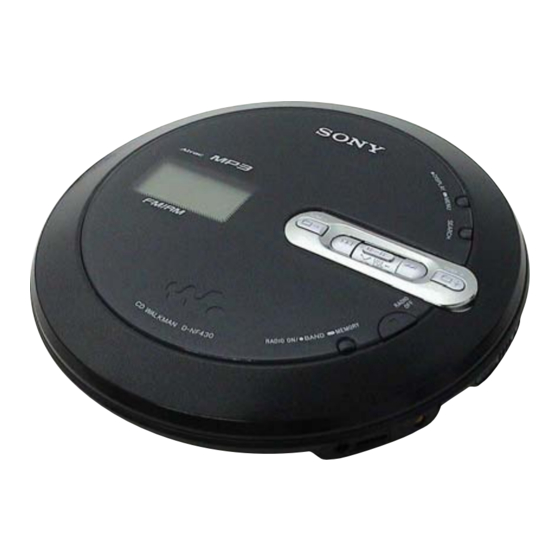
Photo: D-NF430
SPECIFICATIONS
• NF430: US*
9 kHz step:
TV: 2 - 13 ch
WB (weather band): 1 - 7 ch
FM: 87.5 - 108.0 MHz
AM: 531 - 1 710 kHz
10 kHz step:
TV: 2 - 13 ch
WB (weather band): 1 - 7 ch
FM: 87.5 - 108.0 MHz
AM: 530 - 1 710 kHz
* For the area code of the model you purchased,
check the upper left side of the bar code on the
package.
Antenna
FM: Earphones cord antenna
AM: Built-in ferrite bar antenna
General
Power requirements
• LR6 (size AA) battery: 1.5 V DC × 1
• AC power adaptor (DC IN 3 V jack):
230 V, 50 Hz (NF430: UK)
230 V, 50/60 Hz (NF431)
Operating temperature
5°C - 35°C (41°F - 95°F)
Dimensions (w/h/d) (excluding projecting parts
and controls)
Approx. 137.8 × 31.1 × 137.8 mm
1
× 1
1
× 5
1
(5
⁄
⁄
⁄
in.)
2
4
2
Model Name Using Similar Mechanism
CD Mechanism Type
Optical Pick-up Name
Mass (excluding accessories)
Approx. 205 g (7.3 oz.)
Supplied Accessories
AC power adaptor (NF430: UK/NF431)
Earphones
Remote (NF430: US/NF431)
Operating instractions
US and foreign patents licensed from Dolby
Laboratories.
MPEG Layer-3 audio coding technology and patents
licensed from Fraunhofer IIS and Thomson.
Design and specifications are subject to change
without notice.
PORTABLE CD PLAYER
US Model
UK Model
D-NF430
E Model
D-NF431
D-NF420/NF421
CDM-3325ERV2
DAX-25EV
– Continued on next page –
Table of Contents

Related Manuals for Sony D-NF430


Summary of Contents for Sony D-NF430
- Page 1 Approx. 137.8 × 31.1 × 137.8 mm 10 kHz step: × 1 × 5 ⁄ ⁄ ⁄ in.) FM: 87.5 - 108.0 MHz AM: 530 - 1 710 kHz PORTABLE CD PLAYER Sony Corporation 9-879-983-01 Personal Audio Division 2005L05-1 Published by Sony Engineering Corporation © 2005.12...
- Page 2 Battery life Notes on the AC power adaptor • Disconnect all power sources when the player is When using a Sony alkaline battery LR6 not to be used for a long time. (SG) (produced in Japan) • Use only the AC power adaptor supplied. If your...
-
Page 3: Table Of Contents
D-NF430/NF431 TABLE OF CONTENTS SERVICING NOTES ..........4 GENERAL ..............5 DISASSEMBLY 3-1. Disassembly Flow ............6 3-2. Cabinet Lower Sub Assy, Upper LID Sub Assy ....6 3-3. MAIN Board, Optical Pick-up Assy (CDM-3325ERV2) ............7 3-4. SWITCH Board ............... 7 ELECTRICAL ADJUSTMENTS ...... -
Page 4: Servicing Notes
D-NF430/NF431 SECTION 1 SERVICING NOTES LASER DIODE AND FOCUS SEARCH OPERATION NOTES ON HANDLING THE OPTICAL PICK-UP CHECK BLOCK OR BASE UNIT During normal operation of the equipment, emission of the laser The laser diode in the optical pick-up block may suffer electrostatic... -
Page 5: General
D-NF430/NF431 SECTION 2 This section is extracted from instruction manual. GENERAL CD player: Guide to Parts and (group) − •TUNE − button Remote: Controls (group) − •tune − button CD player > buttons CD player: (group) + •TUNE + button Remote: (group) + •tune + button... -
Page 6: Disassembly
D-NF430/NF431 SECTION 3 DISASSEMBLY • This set can be disassembled in the order shown below. 3-1. DISASSEMBLY FLOW 3-2. CABINET LOWER SUB ASSY, UPPER LID SUB ASSY (Page 6) 3-3. MAIN BOARD, OPTICAL PICK-UP ASSY (CDM-3325ERV2) 3-4. SWITCH BOARD (Page 7) (Page 7) Note: Follow the disassembly procedure in the numerical order given. -
Page 7: Main Board, Optical Pick-Up Assy (Cdm-3325Erv2)
D-NF430/NF431 3-3. MAIN BOARD, OPTICAL PICK-UP ASSY (CDM-3325ERV2) 5 optical pick-up assy 4 insulator (CDM-3325ERV2) 2 two connectors (CN601, CN602) 4 insulator 4 insulator 1 OP flexible board (CN603) 3 MAIN board 3-4. SWITCH BOARD 5 SWITCH board 2 lid cover... -
Page 8: Electrical Adjustments
D-NF430/NF431 SECTION 4 ELECTRICAL ADJUSTMENTS 0 dB=1 µV ): NF430: UK/NF431 AM IF ADJUSTMENT [AM] Adjust for a maximum reading on level meter Setting: T102 620 (621) kHz Function: RADIO Band: AM ): NF430: UK/NF431 MAIN board AM FREQUENCY COVERAGE CONFIRMATION... - Page 9 D-NF430/NF431 Adjustment and Connecting Location: – MAIN Board (Component Side) – AM Tracking T101 CT101 Adjustment T102 L103 AM IF Adjustment TV (7 – 13 ch)/WB Tracking Adjustment (NF430: US) L104 FM/TV (2 – 6 ch) Tracking Adjustment – MAIN Board (Conductor Side) –...
- Page 10 D-NF430/NF431 SECTION 5 DIAGRAMS • Note for Printed Wiring Boards and Schematic Diagrams Note on Printed Wiring Board: Note on Schematic Diagram: • X : parts extracted from the component side. • All capacitors are in µF unless otherwise noted. (p: pF) •...
- Page 11 D-NF430/NF431 • IC Block Diagram – MAIN Board – IC101 TB2132FNG IC250 XC6367A303MRN PHASE VOUT COMPENSATION ERROR AMP COMPARATOR BUFFER/ – – DRIVER AM OSCIN PROGRAM PHASE PWM/PFM COUNTER COMPARATOR FM OSCIN CONTROLER REFERENCE REFERENCE DIVIDER IFIN VOLTAGE WITH RAMP WAVE...
-
Page 12: Main Board (Component Side)
D-NF430/NF431 5-1. PRINTED WIRING BOARD – MAIN Board (Component Side) – :Uses unleaded solder. • Semiconductor Location MAIN BOARD (COMPONENT SIDE) Ref. No. Location D251 D402 D403 Q101 L108 Q102 C146 Q401 Q402 C403 Q404 R133 L404 L250 M602 (SLED) -
Page 13: Main Board (Conductor Side)
D-NF430/NF431 5-2. PRINTED WIRING BOARD – MAIN Board (Conductor Side) – :Uses unleaded solder. • Semiconductor Location MAIN BOARD (CONDUCTOR SIDE) Ref. No. Location T103 T101 DC/DC D101 CONVERTER D107 D102 R123 D103 C144 C110 D104 C233 Q104 D105 C155... -
Page 14: Schematic Diagram - Main Board (1/4)
D-NF430/NF431 5-3. SCHEMATIC DIAGRAM – MAIN Board (1/4) – • See page 20 for Waveforms. • See page 11 for IC Block Diagrams. • See page 20 for IC Pin Function Description. (1/4) IC603 +2.1V REGULATOR XC6213B212NR CB605 R604 C607... -
Page 15: Schematic Diagram - Main Board (2/4)
D-NF430/NF431 5-4. SCHEMATIC DIAGRAM – MAIN Board (2/4) – • See page 20 for Waveforms. • See page 20 for IC Pin Function Description. (2/4) R630 R801 CN603 R426 470k OPGUP OPGSW Q407 C609 2SA1832FV 2200p C405 RFACI (TH3SONY) 0.22... -
Page 16: Schematic Diagram - Main Board (3/4)
D-NF430/NF431 5-5. SCHEMATIC DIAGRAM – MAIN Board (3/4) – • See page 20 for Waveforms. • See page 11 for IC Block Diagrams. (3/4) R232 C221 C220 C219 C225 0.22 R276 C131 220p R275 C226 FM_ANT 0.47 ∗C207 C206 C205... -
Page 17: Schematic Diagram - Main Board (4/4)
D-NF430/NF431 5-6. SCHEMATIC DIAGRAM – MAIN Board (4/4) – • See page 20 for Waveforms. • See page 11 for IC Block Diagrams. (4/4) Q104 T103 2SC4154TP-1F DC/DC R115 R121 D108 DC/DC 1SS355TE-17 CONVERTER CONVERTER C144 TP111 (VT) C129 0.01... -
Page 18: Printed Wiring Board - Switch Board
D-NF430/NF431 5-7. PRINTED WIRING BOARD – SWITCH Board – :Uses unleaded solder. SWITCH BOARD S1103 DISPLAY VDR1002 MEMU R1009 R1113 R1114 R1112 R1111 CN1001 R1006 R1004 R1003 S1111 R1002 SEARCH R1001 R1005 LCD1001 LIQUID CRYSTAL DISPLAY R1008 R1101 S1109 U VOL +... -
Page 19: Schematic Diagram - Switch Board
D-NF430/NF431 5-8. SCHEMATIC DIAGRAM – SWITCH Board – CN1001 CN1002 R1001 CLK_I R1002 LCD_CS_I R1003 DATA_O R1004 DATA_I R1009 R1005 RSTB LCD_XRST R1006 VCC2 2.1V VCC3 2.7V VDR1002 (Page 14) VREF DGND VCIN AD_KEY1 SGND C1003 R1007 LCD1001 0.22 LIQUID CRYSTAL... - Page 20 D-NF430/NF431 • Waveforms • IC Pin Function Description – MAIN Board – MAIN BOARD IC401 TB2169AFG (O) (FOCUS/TRACKING COIL DRIVE, SPINDLE/SLED MOTOR DRIVE, POWER CONTROL) IC801 tg (XTAL) IC101 qg (X_O) (FM mode) Pin No. Pin Name Description FG signal output to the system controller...
- Page 21 D-NF430/NF431 Pin No. Pin Name Description Power supply terminal (for tracking coil drive) Tracking coil drive signal (+) output terminal MGND12 Ground terminal (for tracking coil drive and sled motor drive) Sled motor drive signal (-) output terminal Power supply terminal (for sled motor drive)
- Page 22 D-NF430/NF431 MAIN BOARD IC801 CXR721260-203R (SYSTEM CONTROLLER, DSP, LCD DRIVER) Pin No. Pin Name Description Clock signal input terminal Not used Mode select signal input terminal Not used Data input terminal Not used XTRST Reset signal input terminal Not used DVDBK Power supply terminal (+1.2V) (for back up core)
- Page 23 D-NF430/NF431 Pin No. Pin Name Description TESTMODE Not used Not used 49, 50 TEST 3, TEST 2 Not used AVDPLL1 Power supply terminal (+2.6V) (for PLL) AVSPLL1 Ground terminal AVDPLL0 Power supply terminal (+2.6V) (for PLL) AVSMO Ground terminal XTAL System clock output terminal (22.496 MHz)
- Page 24 D-NF430/NF431 Pin No. Pin Name Description VCTL VCO control voltage input terminal for the wideband EFM PLL AVDVCO Power supply terminal (+2V) (for VCO) VPCO Charge pump output terminal for the wideband EFM PLL DVDD Power supply terminal (+1.2V) (for core)
-
Page 25: Exploded Views
D-NF430/NF431 SECTION 6 EXPLODED VIEWS NOTE: • -XX and -X mean standardized parts, so they • Items marked “*” are not stocked since they The components identified by mark may have some difference from the original are seldom required for routine service. Some 0 or dotted line with mark 0 are one. -
Page 26: Cabinet Lower Section
D-NF430/NF431 6-2. CABINET LOWER SECTION not supplied CDM-3325ERV2 MAIN board (NF430: US) Ref. No. Part No. Description Remark Ref. No. Part No. Description Remark X-2102-990-1 CABINET LOWER SUB ASSY (for BLACK) X-2108-145-1 MAIN BOARD, COMPLETE (for SERVICE) X-2102-992-1 CABINET LOWER SUB ASSY (for BLUE) -
Page 27: Optical Pick-Up Section (Cdm-3325Erv2)
D-NF430/NF431 6-3. OPTICAL PICK-UP SECTION (CDM-3325ERV2) M601 M602 Ref. No. Part No. Description Remark Ref. No. Part No. Description Remark 3-318-203-61 SCREW (B1.7X4), TAPPING 3-221-475-01 SHAFT, STANDARD 0 102 X-3383-995-1 OPTICAL PICK-UP (DAX-25EV) 3-222-298-01 RACK 3-221-473-01 COVER, GEAR 3-222-299-01 SPRING, RACK RETAINER 3-221-472-02 CHASSIS 3-348-998-31 SCREW (M1.4X2.5), TAPPING, PAN... -
Page 28: Electrical Parts List
D-NF430/NF431 SECTION 7 MAIN ELECTRICAL PARTS LIST NOTE: • Items marked “*” are not stocked since they • Due to standardization, replacements in the The components identified by mark 0 or dotted line with mark 0 are parts list may be different from the parts are seldom required for routine service. - Page 29 D-NF430/NF431 MAIN Ref. No. Part No. Description Remark Ref. No. Part No. Description Remark C224 1-165-884-11 CERAMIC CHIP 2.2uF 6.3V C437 1-164-874-11 CERAMIC CHIP 100PF C225 1-165-887-11 CERAMIC CHIP 0.22uF 6.3V C226 1-100-415-11 CERAMIC CHIP 0.47uF 6.3V C438 1-164-937-11 CERAMIC CHIP 0.001uF...
- Page 30 D-NF430/NF431 MAIN Ref. No. Part No. Description Remark Ref. No. Part No. Description Remark C883 1-125-777-11 CERAMIC CHIP 0.1uF FB203 1-414-813-11 FERRITE, EMI (SMD) (2012) FB204 1-414-813-11 FERRITE, EMI (SMD) (2012) C891 1-119-750-11 TANTALUM CHIP 22uF 6.3V FB205 1-414-813-11 FERRITE, EMI (SMD) (2012)
- Page 31 D-NF430/NF431 MAIN Ref. No. Part No. Description Remark Ref. No. Part No. Description Remark L412 1-400-145-21 INDUCTOR 47uH R131 1-218-945-11 RES-CHIP 1/16W R132 1-218-990-11 SHORT CHIP 0 (NF430: UK/NF431) L413 1-400-784-21 INDUCTOR 4.7uH (NF430: US) R133 1-216-864-11 SHORT CHIP L414 1-400-784-21 INDUCTOR 4.7uH (NF430: US)
- Page 32 D-NF430/NF431 MAIN Ref. No. Part No. Description Remark Ref. No. Part No. Description Remark R803 1-218-977-11 RES-CHIP 100K 1/16W R433 1-218-990-11 SHORT CHIP R805 1-216-295-00 SHORT CHIP R434 1-218-990-11 SHORT CHIP R809 1-218-990-11 SHORT CHIP R435 1-218-990-11 SHORT CHIP R810...
- Page 33 D-NF430/NF431 SWITCH Ref. No. Part No. Description Remark Ref. No. Part No. Description Remark A-1152-105-A SWITCH BOARD, COMPLETE < SWITCH > *********************** S1101 1-786-650-21 SWITCH, TACTILE (u) 1-831-830-11 FLEXIBLE FLAT CABLE (10 CORE ) S1102 1-786-650-21 SWITCH, TACTILE(RADIO ON/BAND, MEMORY)
- Page 34 D-NF430/NF431 REVISION HISTORY Clicking the version allows you to jump to the revised page. Also, clicking the version at the upper right on the revised page allows you to jump to the next revised page. Ver. Date Description of Revision...