Table of Contents
Quick Links
CC2652PSIP SimpleLink™ Multiprotocol 2.4-GHz Wireless System-in-Package
1 Features
Wireless microcontroller
•
Powerful 48-MHz Arm® Cortex®-M4F processor
•
352KB flash program memory
•
256KB of ROM for protocols and library functions
•
8KB of cache SRAM
•
80KB of ultra-low leakage SRAM with parity for
high-reliability operation
•
Dynamic multiprotocol manager (DMM) driver
•
Programmable radio includes support for 2-
(G)FSK, 4-(G)FSK, MSK, OOK, Bluetooth® 5.2
Low Energy, IEEE 802.15.4 PHY and MAC
•
Supports over-the-air upgrade (OTA)
Ultra-low power sensor controller
•
Autonomous MCU with 4KB of SRAM
•
Sample, store, and process sensor data
•
Fast wake-up for low-power operation
•
Software defined peripherals; capacitive touch,
flow meter, LCD
Low power consumption
•
MCU consumption:
– 3.5 mA active mode, CoreMark
– 74 μA/MHz running CoreMark
– 1 μA standby mode, RTC, 80KB RAM
– 160 nA shutdown mode, wake-up on pin
•
Ultra low-power sensor controller consumption:
– 30.1 μA in 2 MHz mode
– 808 μA in 24 MHz mode
•
Radio Consumption:
– 7.3 mA RX at 2.4 GHz
– 7.9 mA TX at 0 dBm
– 10.9 mA TX at +5 dBm
– 33 mA TX at +10 dBm
Wireless protocol support
•
Thread, Zigbee®,
Matter
•
Bluetooth® 5.2 Low Energy
•
SimpleLink™ TI 15.4-stack
•
Proprietary systems
High performance radio
•
-103 dBm sensitivity for Bluetooth® Low Energy
125-kbps LE Coded PHY
•
Output power up to +10 dBm with temperature
compensation
An IMPORTANT NOTICE at the end of this data sheet addresses availability, warranty, changes, use in safety-critical applications,
intellectual property matters and other important disclaimers. PRODUCTION DATA.
With Integrated Power Amplifier
Regulatory compliance
•
MCU peripherals
•
•
•
•
•
•
•
•
•
Security enablers
•
•
•
•
Development tools and software
•
•
•
•
•
Operating range
•
•
•
Package
•
•
SWRS263A – FEBRUARY 2021 – REVISED JUNE 2022
Regulatory certification for compliance with
worldwide radio frequency:
– ETSI RED (Europe)
– ISED (Canada)
– FCC (USA)
Digital peripherals can be routed to any of 30
GPIOs
Four 32-bit or eight 16-bit general-purpose timers
12-bit ADC, 200 kSamples/s, 8 channels
8-bit DAC
Two comparators
Programmable current source
2
Two UART, two SSI, I
C, I
Real-time clock (RTC)
Integrated temperature and battery monitor
AES 128- and 256-bit cryptographic accelerator
ECC and RSA public key hardware accelerator
SHA2 Accelerator (full suite up to SHA-512)
True random number generator (TRNG)
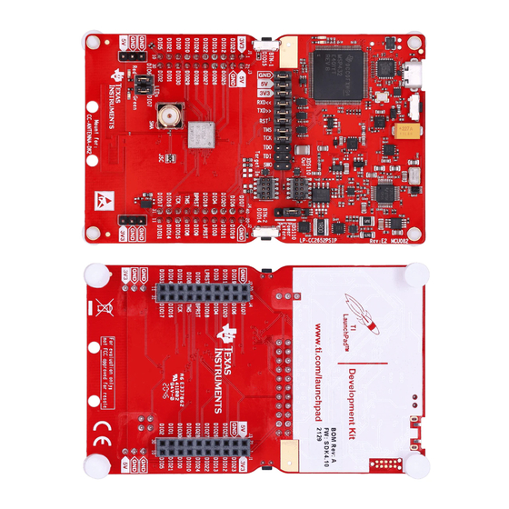
LP-CC2652RSIP Development Kit
SimpleLink™ CC13xx and CC26xx Software
Development Kit (SDK)
SmartRF™ Studio
for simple radio configuration
Sensor Controller Studio for building low-power
sensing applications
SysConfig
system configuration tool
On-chip buck DC/DC converter
1.8-V to 3.8-V single supply voltage
T
: -40 to +105°C
j
7-mm × 7-mm MOT (30 GPIOs)
RoHS-compliant package
CC2652PSIP
2
S
Table of Contents

Related Manuals for Texas Instruments SimpleLink CC2652PSIP


Summary of Contents for Texas Instruments SimpleLink CC2652PSIP
-
Page 1: Features
CC2652PSIP SWRS263A – FEBRUARY 2021 – REVISED JUNE 2022 CC2652PSIP SimpleLink™ Multiprotocol 2.4-GHz Wireless System-in-Package With Integrated Power Amplifier Regulatory compliance 1 Features • Regulatory certification for compliance with Wireless microcontroller worldwide radio frequency: • Powerful 48-MHz Arm® Cortex®-M4F processor –... -
Page 2: Applications
For the most current part, package, and ordering information for all available devices, see the Package Option Addendum in Section 13, or see the website. RF Core for additional details on supported protocol standards, modulation formats, and data rates. Submit Document Feedback Copyright © 2022 Texas Instruments Incorporated Product Folder Links: CC2652PSIP... -
Page 3: Functional Block Diagram
(1.8 V to 3.8 V) VDDS_PU +10-dBm RESET_N CC2652P User DIO_0-31 Switch (50 , 2.4 GHz) +5-dBm (1.8 V to 3.8 V) VDDS DCDC Passives Figure 4-1. CC2652PSIP Block Diagram Copyright © 2022 Texas Instruments Incorporated Submit Document Feedback Product Folder Links: CC2652PSIP... - Page 4 CC2652PSIP www.ti.com SWRS263A – FEBRUARY 2021 – REVISED JUNE 2022 Figure 4-2 shows an overview of the CC2652PSIP hardware. Figure 4-2. CC2652PSIP Hardware Overview Submit Document Feedback Copyright © 2022 Texas Instruments Incorporated Product Folder Links: CC2652PSIP...
-
Page 5: Table Of Contents
Updated numbering of sections, figures, and tables throughout the data sheet..........1 • Updated formatting throughout data sheet to match current documentation standards........1 • Devices are now PRODUCTION DATA......................Copyright © 2022 Texas Instruments Incorporated Submit Document Feedback Product Folder Links: CC2652PSIP... -
Page 6: Device Comparison
RADIO SUPPORT Certifications Package Size FLASH RAM + Module GPIO (KB) Cache (KB) CC2650MODA 20+8 CC2651R3SIPA 32 + 8 CC2652RSIP 80 + 8 CC2652PSIP 80 + 8 Submit Document Feedback Copyright © 2022 Texas Instruments Incorporated Product Folder Links: CC2652PSIP... -
Page 7: Terminal Configuration And Functions
Pin 2, DIO_27 • Pin 3, DIO_28 • Pin 7, DIO_29 • Pin 8, DIO_30 • Pin 44, DIO_23 • Pin 45, DIO_24 • Pin 48, DIO_25 Copyright © 2022 Texas Instruments Incorporated Submit Document Feedback Product Folder Links: CC2652PSIP... -
Page 8: Signal Descriptions - Sip Package
— — — — — — — — — — — — — — — — 49-73 — — — — No Connect — — No Connect Submit Document Feedback Copyright © 2022 Texas Instruments Incorporated Product Folder Links: CC2652PSIP... -
Page 9: Connections For Unused Pins And Modules
Table 7-2. Connections for Unused Pins – SIP Package PREFERRED FUNCTION SIGNAL NAME PIN NUMBER ACCEPTABLE PRACTICE PRACTICE GPIO DIO_n 20-33 NC or GND 36-45 No Connects 6, 14-15 NC = No connect Copyright © 2022 Texas Instruments Incorporated Submit Document Feedback Product Folder Links: CC2652PSIP... -
Page 10: Specifications
VDDS Brown-out Detector (BOD) Falling threshold 1.75 Brown-out Detector is trimmed at initial boot, value is kept until device is reset by a POR reset or the nRESET pin Submit Document Feedback Copyright © 2022 Texas Instruments Incorporated Product Folder Links: CC2652PSIP... -
Page 11: Power Consumption - Power Modes
Low-power mode 2 MHz, infinite loop 30.1 CC2652xSIP integrates a 100 kΩ pull-up resistor on nRESET Only one UART running Only one SSI running Only one GPTimer running Copyright © 2022 Texas Instruments Incorporated Submit Document Feedback Product Folder Links: CC2652PSIP... -
Page 12: Power Consumption - Radio Modes
Junction-to-board characterization parameter 32.0 °C/W For more information about traditional and new thermal metrics, see Semiconductor and IC Package Thermal Metrics. °C/W = degrees Celsius per watt. Submit Document Feedback Copyright © 2022 Texas Instruments Incorporated Product Folder Links: CC2652PSIP... -
Page 13: Rf Frequency Bands
46 / 46 –3 MHz, BER = 10 Wanted signal at –72 dBm, modulated interferer at ±4 Selectivity, ±4 MHz 45 / 47 –3 MHz, BER = 10 Copyright © 2022 Texas Instruments Incorporated Submit Document Feedback Product Folder Links: CC2652PSIP... - Page 14 > (–500 / 500) the internally generated carrier frequency Difference between incoming data rate and the internally Data rate error tolerance > (–700 / 750) generated data rate (37-byte packets) Submit Document Feedback Copyright © 2022 Texas Instruments Incorporated Product Folder Links: CC2652PSIP...
- Page 15 Suitable for systems targeting compliance with worldwide radio-frequency regulations ETSI EN 300 328 and EN 300 440 Class 2 (Europe), FCC CFR47 Part 15 (US), and ARIB STD-T66 (Japan) Copyright © 2022 Texas Instruments Incorporated Submit Document Feedback Product Folder Links:...
-
Page 16: Bluetooth Low Energy - Transmit (Tx)
To meet the ETSI EN 300 328 (Europe) 10 dBm/MHz Power Spectral Density (PSD) requirement, output power is limited to 7 dBm and 6dBm when using a max antenna gain of 1.9 dBi and 3.3 dBi, respectively. Submit Document Feedback Copyright © 2022 Texas Instruments Incorporated Product Folder Links: CC2652PSIP... -
Page 17: Zigbee And Thread - Ieee 802.15.4-2006 2.4 Ghz (Oqpsk Dsss1:8, 250 Kbps) - Rx
Difference between incoming symbol rate and the internally Symbol rate error tolerance > 1000 generated symbol rate RSSI dynamic range RSSI accuracy ±4 Copyright © 2022 Texas Instruments Incorporated Submit Document Feedback Product Folder Links: CC2652PSIP... -
Page 18: Zigbee And Thread - Ieee 802.15.4-2006 2.4 Ghz (Oqpsk Dsss1:8, 250 Kbps) - Tx
To meet the FCC 15.247 Part 15 (US) Band Edge requirement, Channel 16 is reduced by 3 dBm. 8.14 Timing and Switching Characteristics 8.14.1 Reset Timing PARAMETER UNIT nRESET low duration µs Submit Document Feedback Copyright © 2022 Texas Instruments Incorporated Product Folder Links: CC2652PSIP... - Page 19 = 3.0 V at initial time, unless otherwise noted. UNIT Crystal frequency 32.768 Initial crystal frequency tolerance Crystal aging at 1st year ppm/year External manufacturer's crystal specification Copyright © 2022 Texas Instruments Incorporated Submit Document Feedback Product Folder Links: CC2652PSIP...
- Page 20 When using the TI-provided Power driver, the SSI system clock is always 48 MHz. SSIClk SSIFss SSITx SSIRx 4 to 16 bits Figure 8-1. SSI Timing for TI Frame Format (FRF = 01), Single Transfer Timing Measurement Submit Document Feedback Copyright © 2022 Texas Instruments Incorporated Product Folder Links: CC2652PSIP...
- Page 21 (SPO = 0) SSIClk (SPO = 1) SSITx (Controller) SSIRx (Peripheral) SSIFss Figure 8-3. SSI Timing for SPI Frame Format (FRF = 00), With SPH = 1 Copyright © 2022 Texas Instruments Incorporated Submit Document Feedback Product Folder Links: CC2652PSIP...
- Page 22 SWRS263A – FEBRUARY 2021 – REVISED JUNE 2022 8.14.5 UART Table 8-1. UART Characteristics over operating free-air temperature range (unless otherwise noted) PARAMETER UNIT UART rate MBaud Submit Document Feedback Copyright © 2022 Texas Instruments Incorporated Product Folder Links: CC2652PSIP...
-
Page 23: Peripheral Characteristics
= 4.3 V × 1408 / 4095 Reference voltage VDDS as reference, input voltage scaling enabled VDDS VDDS / Reference voltage VDDS as reference, input voltage scaling disabled 2.82 Copyright © 2022 Texas Instruments Incorporated Submit Document Feedback Product Folder Links: CC2652PSIP... - Page 24 ±0.81 Offset error = VDDS = 1.8 V ±1.27 Load = Continuous Time = DCOUPL, pre-charge ON ±3.43 Comparator = DCOUPL, pre-charge OFF ±2.88 = ADCREF ±2.37 Submit Document Feedback Copyright © 2022 Texas Instruments Incorporated Product Folder Links: CC2652PSIP...
- Page 25 = 250 kHz ±1 Integral nonlinearity = DCOUPL, F = 250 kHz ±1 = ADCREF, F = 250 kHz ±1 Differential nonlinearity = VDDS, F = 250 kHz ±1 Copyright © 2022 Texas Instruments Incorporated Submit Document Feedback Product Folder Links: CC2652PSIP...
- Page 26 3.8 V/3.0 V/1.8 V/DCOUPL/ADCREF) = 14.10 mV/11.13 mV/6.68 mV/4.67 mV/5.48 mV Includes comparator offset A load > 20 pF will increases the settling time Keysight 34401A Multimeter Submit Document Feedback Copyright © 2022 Texas Instruments Incorporated Product Folder Links: CC2652PSIP...
- Page 27 CC2652PSIP www.ti.com SWRS263A – FEBRUARY 2021 – REVISED JUNE 2022 8.15.3 Temperature and Battery Monitor 8.15.3.1 Temperature Sensor Measured on a Texas Instruments reference design with T = 25 °C, V = 3.0 V, unless otherwise noted. PARAMETER TEST CONDITIONS...
- Page 28 = 25 °C, V = 3.0 V, unless otherwise noted. PARAMETER TEST CONDITIONS UNIT Current source programmable output range (logarithmic 0.25 - 20 µA range) Resolution 0.25 µA Submit Document Feedback Copyright © 2022 Texas Instruments Incorporated Product Folder Links: CC2652PSIP...
- Page 29 1 → 0 points = 25 °C Lowest GPIO input voltage reliably interpreted as a 0.8*V High Highest GPIO input voltage reliably interpreted as a 0.2*V Copyright © 2022 Texas Instruments Incorporated Submit Document Feedback Product Folder Links: CC2652PSIP...
-
Page 30: Typical Characteristics
Temperature [ Voltage [V] Figure 8-6. RX Current vs. Temperature Figure 8-7. RX Current vs. Supply Voltage (VDDS) (BLE 1 Mbps, 2.44 GHz) (BLE 1 Mbps, 2.44 GHz) Submit Document Feedback Copyright © 2022 Texas Instruments Incorporated Product Folder Links: CC2652PSIP... - Page 31 (BLE 1 Mbps, 2.44 GHz, +5 dBm) (BLE 1 Mbps, 2.44 GHz, +10 dBm PA) shows typical TX current and output power for different output power settings. Copyright © 2022 Texas Instruments Incorporated Submit Document Feedback Product Folder Links: CC2652PSIP...
- Page 32 0x26E0 -3.04 7.19 0x0ED8 -5.10 6.65 0x08E5 -6.32 6.41 0x08D0 -9.28 5.94 0x08CF -9.96 5.85 0x00CC -12.11 5.61 0c00C9 -15.29 5.34 0c08C7 -18.79 5.12 0c08C6 -20.25 5.05 Submit Document Feedback Copyright © 2022 Texas Instruments Incorporated Product Folder Links: CC2652PSIP...
- Page 33 Voltage [V] Figure 8-18. Sensitivity vs. Supply Voltage Figure 8-19. Sensitivity vs. Supply Voltage (VDDS) (BLE 1 Mbps, 2.44 GHz) (VDDS) (BLE 1 Mbps, 2.44 GHz, DCDC Off) Copyright © 2022 Texas Instruments Incorporated Submit Document Feedback Product Folder Links: CC2652PSIP...
- Page 34 SWRS263A – FEBRUARY 2021 – REVISED JUNE 2022 -100 -101 -102 -103 -104 Voltage [V] Figure 8-20. Sensitivity vs. Supply Voltage (VDDS) (250 kbps, 2.44 GHz) Submit Document Feedback Copyright © 2022 Texas Instruments Incorporated Product Folder Links: CC2652PSIP...
- Page 35 Figure 8-25. Output Power vs. Supply Voltage Figure 8-26. Output Power vs. Supply Voltage (VDDS) (BLE 1 Mbps, 2.44 GHz, +5 dBm) (VDDS) (2.44 GHz, +10 dBm PA) Copyright © 2022 Texas Instruments Incorporated Submit Document Feedback Product Folder Links: CC2652PSIP...
- Page 36 +7 dBm +6 dBm 2.408 2.416 2.424 2.432 2.44 2.448 2.456 2.464 2.472 2.48 Frequency [GHz] Figure 8-29. Output Power vs. Frequency (BLE 1Mbps, +10 dBm PA) Submit Document Feedback Copyright © 2022 Texas Instruments Incorporated Product Folder Links: CC2652PSIP...
- Page 37 1.003 1.002 1.002 1.001 1.001 -40 -30 -20 -10 Voltage [V] Temperature [°C] Figure 8-35. ADC Accuracy vs. Supply Voltage Figure 8-34. ADC Accuracy vs. Temperature (VDDS) Copyright © 2022 Texas Instruments Incorporated Submit Document Feedback Product Folder Links: CC2652PSIP...
-
Page 38: Detailed Description
Tightly connected to 8-KB 4-way random replacement cache for minimal active power consumption and wait states • Ultra-low-power consumption with integrated sleep modes • 48 MHz operation • 1.25 DMIPS per MHz Submit Document Feedback Copyright © 2022 Texas Instruments Incorporated Product Folder Links: CC2652PSIP... -
Page 39: Radio (Rf Core)
8-KB cache is enabled by default to cache and prefetch instructions read by the system CPU. The cache can be used as a general-purpose RAM by enabling this feature in the Customer Configuration Area (CCFG). Copyright © 2022 Texas Instruments Incorporated Submit Document Feedback Product Folder Links:... - Page 40 The ROM also contains a serial (SPI and UART) bootloader that can be used for initial programming of the device. Submit Document Feedback Copyright © 2022 Texas Instruments Incorporated Product Folder Links: CC2652PSIP...
-
Page 41: Sensor Controller
The analog modules can connect to up to eight different GPIOs • Dedicated SPI controller with up to 6 MHz clock speed The peripherals in the Sensor Controller can also be controlled from the main application processor. Copyright © 2022 Texas Instruments Incorporated Submit Document Feedback Product Folder Links: CC2652PSIP... -
Page 42: Cryptography
Other capabilities, such as RSA encryption and signatures as well as Edwards type of elliptic curves such as Curve1174 or Ed25519, can also be implemented using the provided hardware accelerators but are not part of the TI SimpleLink SDK for the CC2652PSIP device. Submit Document Feedback Copyright © 2022 Texas Instruments Incorporated Product Folder Links: CC2652PSIP... -
Page 43: Timers
The watchdog timer runs on a 1.5 MHz clock rate and cannot be stopped once enabled. The watchdog timer pauses to run in Standby power mode and when a debugger halts the device. Copyright © 2022 Texas Instruments Incorporated Submit Document Feedback Product Folder Links:... -
Page 44: Serial Peripherals And I/O
The on-chip debug support is done through a dedicated cJTAG (IEEE 1149.7) or JTAG (IEEE 1149.1) interface. The device boots by default into cJTAG mode and must be reconfigured to use 4-pin JTAG. Submit Document Feedback Copyright © 2022 Texas Instruments Incorporated Product Folder Links: CC2652PSIP... -
Page 45: Power Management
The only state retained in this mode is the latched I/O state and the flash memory contents. Copyright © 2022 Texas Instruments Incorporated Submit Document Feedback... -
Page 46: Clock Systems
In the first case, the external host MCU communicates with the device using SPI or UART. In the second case, the application must be written according to the application framework supplied with the wireless protocol stack. Submit Document Feedback Copyright © 2022 Texas Instruments Incorporated Product Folder Links: CC2652PSIP... -
Page 47: Device Certification And Qualification
• This device may not cause harmful interference. • This device must accept any interference received, including interference that may cause undesired operation of the device. Copyright © 2022 Texas Instruments Incorporated Submit Document Feedback Product Folder Links: CC2652PSIP... - Page 48 Declaration of Conformity and evidenced by the UK mark. The module is tested and certified against the Radio Equipment Regulations 2017. See the full text of the for the UK Declaration of Conformity for the CC2652PSIPMOT device. Submit Document Feedback Copyright © 2022 Texas Instruments Incorporated Product Folder Links: CC2652PSIP...
-
Page 49: Module Markings
RF module in the user’s manual of the end product which integrates this module. The end user manual must include all required regulatory information and warnings as shown in this manual. Copyright © 2022 Texas Instruments Incorporated Submit Document Feedback... -
Page 50: Application, Implementation, And Layout
PCB to account for PCB parasitics. Please refer to CC13xx/CC26xx Hardware Configuration and PCB Design Considerations; section 5.1 for further information. Figure 10-1. CC2652PSIP Typical Application Schematic Submit Document Feedback Copyright © 2022 Texas Instruments Incorporated Product Folder Links: CC2652PSIP... -
Page 51: Device Connection And Layout Fundamentals
Have a solid ground plane and ground vias under the module for stable system and thermal dissipation. • Do not run signal traces underneath the module on a layer where the module is mounted. Copyright © 2022 Texas Instruments Incorporated Submit Document Feedback Product Folder Links:... - Page 52 RF traces must be as short as possible. • The module must be as close to the PCB edge in consideration of the product enclosure and type of antenna being used. Submit Document Feedback Copyright © 2022 Texas Instruments Incorporated Product Folder Links: CC2652PSIP...
- Page 53 Table 10-3. Recommended Components CHOICE ANTENNA MANUFACTURER NOTES 2.4-GHz Inverted F Refer to 2.4-GHz Inverted F Antenna for details of the Antenna Texas Instruments Antenna implementation and PCB requirements. Copyright © 2022 Texas Instruments Incorporated Submit Document Feedback Product Folder Links: CC2652PSIP...
- Page 54 GND and via stitching. Figure 10-3. Coplanar Waveguide (Cross Section) Figure 10-4. CPW With GND and Via Stitching (Top View) Submit Document Feedback Copyright © 2022 Texas Instruments Incorporated Product Folder Links: CC2652PSIP...
-
Page 55: Reference Designs
Dual-band antennas for 868 MHz and 915 MHz combined with 2.4 GHz The antenna kit includes a JSC cable to connect to the Wireless MCU LaunchPad Development Kits and SensorTags. Copyright © 2022 Texas Instruments Incorporated Submit Document Feedback Product Folder Links:... -
Page 56: Environmental Requirements And Smt Specifications
Monitor the solder paste volume (uniformity) • Package placement using standard SMT placement equipment • X-ray pre-reflow check - paste bridging • Reflow • X-ray post-reflow check - solder bridging and voids Submit Document Feedback Copyright © 2022 Texas Instruments Incorporated Product Folder Links: CC2652PSIP... -
Page 57: Baking Conditions
Humidity indicator cards read > 30% • Temp < 30°C, humidity < 70% RH, over 96 hours Baking condition: 90°C, 12 to 24 hours Baking times: 1 time Copyright © 2022 Texas Instruments Incorporated Submit Document Feedback Product Folder Links: CC2652PSIP... -
Page 58: Soldering And Reflow Condition
This coating can lead to localized stress on the solder connections inside the module and impact the module reliability. Use caution during the module assembly process to the final PCB to avoid the presence of foreign material inside the module. Submit Document Feedback Copyright © 2022 Texas Instruments Incorporated Product Folder Links: CC2652PSIP... -
Page 59: Device And Documentation Support
Predictions show that prototype devices (X or P) have a greater failure rate than the standard production devices. Texas Instruments recommends that these devices not be used in any production system because their expected end-use failure rate still is undefined. Only qualified production devices are to be used. - Page 60 For more information about the SimpleLink MCU Platform, visit http://www.ti.com/simplelink. Submit Document Feedback Copyright © 2022 Texas Instruments Incorporated Product Folder Links: CC2652PSIP...
- Page 61 Studio SimpleLink Wireless MCUs from Texas Instruments. The application will help designers of RF systems to easily evaluate the radio at an early stage in the design process. It is especially useful for generation of configuration register values and for practical testing and debugging of the RF system.
-
Page 62: Documentation Support
, and TI E2E are trademarks of Texas Instruments. I-jet ™ is a trademark of IAR Systems AB. J-Link ™ is a trademark of SEGGER Microcontroller Systeme GmbH. Submit Document Feedback Copyright © 2022 Texas Instruments Incorporated Product Folder Links: CC2652PSIP... -
Page 63: Electrostatic Discharge Caution
All trademarks are the property of their respective owners. 12.6 Electrostatic Discharge Caution This integrated circuit can be damaged by ESD. Texas Instruments recommends that all integrated circuits be handled with appropriate precautions. Failure to observe proper handling and installation procedures can cause damage. -
Page 64: Mechanical, Packaging, And Orderable Information
For browser-based versions of this data sheet, refer to the left-hand navigation. Note The total height of the module is 1.51 mm. The weight of the CC2652PSIP module is typically 0.186 g. Submit Document Feedback Copyright © 2022 Texas Instruments Incorporated Product Folder Links: CC2652PSIP... - Page 65 CC2652PSIP www.ti.com SWRS263A – FEBRUARY 2021 – REVISED JUNE 2022 Copyright © 2022 Texas Instruments Incorporated Submit Document Feedback Product Folder Links: CC2652PSIP...
- Page 66 CC2652PSIP www.ti.com SWRS263A – FEBRUARY 2021 – REVISED JUNE 2022 Submit Document Feedback Copyright © 2022 Texas Instruments Incorporated Product Folder Links: CC2652PSIP...
- Page 67 CC2652PSIP www.ti.com SWRS263A – FEBRUARY 2021 – REVISED JUNE 2022 Copyright © 2022 Texas Instruments Incorporated Submit Document Feedback Product Folder Links: CC2652PSIP...
- Page 68 TI products. TI’s provision of these resources does not expand or otherwise alter TI’s applicable warranties or warranty disclaimers for TI products. TI objects to and rejects any additional or different terms you may have proposed. IMPORTANT NOTICE Mailing Address: Texas Instruments, Post Office Box 655303, Dallas, Texas 75265 Copyright © 2022, Texas Instruments Incorporated...