JVC XV-S40BK Service Manual
Dvd video player
Hide thumbs
Also See for XV-S40BK:
- Service manual (77 pages) ,
- Instructions manual (55 pages) ,
- Instructions manual (53 pages)
Quick Links
SERVICE MANUAL
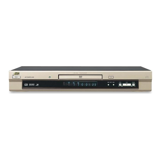
XV-S40BK / XV-S42SL
XV-S45GD / XV-S30BK
˚
Each difference point
Model
XV-S40BK
XV-S42SL
XV-S45GD
XV-S30BK
Contents
Safety precautions ------------------------ 1-2
Preventing static electricity ------------- 1-3
Importance admistering
point on the safety ------------ 1-4
DVD VIDEO PLAYER
Body color
Optical digital out
Black
O
Silver
O
Gold
O
Black
X
Precautions for service ----------------- 1-5
Disassembly method -------------------- 1-6
Adjustment method ---------------------- 1-15
Description of major ICs ---------------- 1-21
This service manual is printed on 100% recycled paper.
COPYRIGHT
2001 VICTOR COMPANY OF JAPAN, LTD.
XV-S40BK/XV-S42SL
XV-S45GD/XV-S30BK
Area Suffix
(XV-S40BK/XV-S30BK)
J ------------- U.S.A.
C ---------- Canada
AV Compulink
O
Area Suffix (XV-S42SL)
O
C ---------- Canada
O
X
Area Suffix (XV-S45GD)
J ------------- U.S.A.
No.A0003
Feb. 2001

Related Manuals for JVC XV-S40BK


Summary of Contents for JVC XV-S40BK
-
Page 1: Table Of Contents
XV-S40BK/XV-S42SL XV-S45GD/XV-S30BK SERVICE MANUAL DVD VIDEO PLAYER XV-S40BK / XV-S42SL XV-S45GD / XV-S30BK ˚ Area Suffix (XV-S40BK/XV-S30BK) Each difference point J ------------- U.S.A. C ---------- Canada Model Body color Optical digital out AV Compulink XV-S40BK Black Area Suffix (XV-S42SL) XV-S42SL... -
Page 2: Safety Precautions
XV-S40BK/XV-S42SL/XV-S45GD/XV-S30BK Safety Precautions 1. This design of this product contains special hardware and many circuits and components specially for safety purposes. For continued protection, no changes should be made to the original design unless authorized in writing by the manufacturer. Replacement parts must be identical to those used in the original circuits. -
Page 3: Preventing Static Electricity
XV-S40BK/XV-S42SL/XV-S45GD/XV-S30BK Preventing static electricity Electrostatic discharge (ESD), which occurs when static electricity stored in the body, fabric, etc. is discharged, can destroy the laser diode in the traverse unit (optical pickup). Take care to prevent this when performing repairs. 1.1. Grounding to prevent damage by static electricity Static electricity in the work area can destroy the optical pickup (laser diode) in devices such as DVD players. -
Page 4: Point On The Safety
XV-S40BK/XV-S42SL/XV-S45GD/XV-S30BK Importance Admistering point on the Safety Full Fuse Replacement Marking Marquage Pour Le Remplacement Complet De Fusible Graphic symbol mark Le symbole graphique (Ce symbole signifie (This symbol means fast blow type fuse.) fusible de type a fusion rapide.) should be read as follows ;... - Page 5 XV-S40BK/XV-S42SL/XV-S45GD/XV-S30BK Precautions for Service Handling of Traverse Unit and Laser Pickup 1. Do not touch any peripheral element of the pickup or the actuator. 2. The traverse unit and the pickup are precision devices and therefore must not be subjected to strong shock.
-
Page 6: Disassembly Method
XV-S40BK/XV-S42SL/XV-S45GD/XV-S30BK Disassembly methodRemoving the top cover (see Fig.1) 1.Remove the two screws A attaching the top cover on both sides of the body. A x 2 2.Remove the three screws B attaching the top cover on the back of the body. - Page 7 XV-S40BK/XV-S42SL/XV-S45GD/XV-S30BK Removing the rear panel (see Fig.5) *Prior to performing the following procedure, remove Rear panel the top cover. 1.Remove the six screws D attaching the rear panel on the back of the body. Removing the front panel assembly Fig.5 (see Fig.6,7)
-
Page 8
XV-S40BK/XV-S42SL/XV-S45GD/XV-S30BK
Removing the clamper assembly Joint a Joint a (See Fig.1) Remove the four screws A attaching the clamper assembly. Move the clamper in the direction of the arrow to release the two joints a on both sides. - Page 9 XV-S40BK/XV-S42SL/XV-S45GD/XV-S30BK Removing the traverse mechanism assembly (See Fig.4 and 5) Prior to performing the following procedure, remove the clamper assembly and the tray. Traverse mechanism Remove the four screws B attaching the traverse assembly mechanism assembly. ATTENTION: Before reattaching the traverse...
- Page 10 XV-S40BK/XV-S42SL/XV-S45GD/XV-S30BK Removing the motor assembly (See Fig.8 and 9) Belt Prior to performing the following procedure, remove the clamper assembly, the tray, the traverse mechanism assembly and the elevator. Remove the belt from the pulley. Remove the screw C attaching the motor assembly.
- Page 11 XV-S40BK/XV-S42SL/XV-S45GD/XV-S30BK Pulley gear Idle gear Pulley gear bracket Pulley gear Idle gear Pulley gear bracket Tads h Pulley gear Motor assembly Fig.10 Slide cam Removing the Idle gear / pulley gear / middle gear / slide cam (See Fig.10 to 12)
-
Page 12
XV-S40BK/XV-S42SL/XV-S45GD/XV-S30BK
Feed motor assembly Removing the feed motor assembly (See Fig.13) Unsolder the two soldering j on the spindle motor board. Remove the two screws F attaching the feed motor assembly. Pickup Notch k Soldering j... - Page 13 XV-S40BK/XV-S42SL/XV-S45GD/XV-S30BK Removing the pickup (See Fig.16 and 17) Pickup Joint n Remove the screw I attaching the T spring (S) and Shaft holder the shaft holder. Remove also the plate. ATTENTION: When reattaching, make sure that the T spring (S) presses the shaft.
- Page 14 XV-S40BK/XV-S42SL/XV-S45GD/XV-S30BK Spindle motor Removing the spindle motor assembly (See Fig.19 to 21) Remove the three screws L attaching the spindle motor on the bottom of the mechanism base. ATTENTION: When reattaching, pass the card wire extending from the spindle motor board through the notch of the spindle base.
-
Page 15: Adjustment Method
XV-S40BK/XV-S42SL/XV-S45GD/XV-S30BK Adjustment method (1) Initialization method If microprocessor (IC401,IC402,IC403) or pick-up is replaces, initialize the DVD player in the following matter 1)Take out the disc and close the tray. 2)Unplug the power plug. 3)Insert power plug into outlet while pressing both PLAY button and OPEN/CLOSE button. - Page 16 XV-S40BK/XV-S42SL/XV-S45GD/XV-S30BK For Jitter value The jitter value is displayed by the hexadecimal number and refer to the conversion table of following,please. If the indication value is 11% or less, it can be judged by this simple checking method that the signal read precision of the set is satisfactory.
- Page 17 XV-S40BK/XV-S42SL/XV-S45GD/XV-S30BK Troubleshooting Servo volume Press OPEN /CLOSE key Is tray Confirmation of tray drive circuit operation and circuit in surrounding correct? Is the traverse moving See "(3) Traverse movement error" along the innermost in "Check points for individual errors" perimeter for SW detection? "NO DISC"...
- Page 18 XV-S40BK/XV-S42SL/XV-S45GD/XV-S30BK Check points for each error (1) Spindle start error 1.Defective spindle motor *Are there several ohms resistance between each pin of CN201 "5-6","6-7","5-7"? (The power supply is turned off and measured.) *Is the sign wave of about 100mVp-p in the voltage had from each terminal? [ CN201"9"(H1-),"10"(H1+),"11"(H2-),"12"(H2+),"13"(H3-),"14"(H3+) ]...
- Page 19 XV-S40BK/XV-S42SL/XV-S45GD/XV-S30BK (3) Traverse movement NG 1.Defective traverse driver *Has the voltage come between terminal of CN101 "1" and "2" ? 2.Defective BTL driver (IC271) *Has the motor drive voltage gone out to IC271"17" or "18"? 3.Has the control signal come from servo IC or the microcomputer? *Is it "H"...
- Page 20 XV-S40BK/XV-S42SL/XV-S45GD/XV-S30BK (9) Neither picture nor sound is output 1.It is not possible to search *Has the tracking been turned on? *To "(5) Tracking ON error" in "Check points for individual errors" when the tracking is not normal. *Is the feed operation normal? To "(3) traverse movement NG"...
-
Page 21: Description Of Major Ics
XV-S40BK/XV-S42SL/XV-S45GD/XV-S30BK Description of major ICs AN8702FH(IC101):Frontend processor 1.Pin layout RFINN PC01 RFINP TESTSG PC02 AGCO TGBAL AGCG TBAL PEAK FBAL BOTTOM AN8702FH POFLT RFENV DTRD IDGT OFTR STANDBY DCRF VCC3 STDI RFOUT RSEL RFDIFO JLINE GND3 2.Pin function Symbol Description... - Page 22 XV-S40BK/XV-S42SL/XV-S45GD/XV-S30BK BA5983FM-X (IC271) : 4CH DRIVER 1.Block Diagram STAND BY Level Shift Level Shift Level Shift Level Shift STAND BY CH1/2/3 2.Pin Function Function Symbol Symbol Function Pin No. Pin No. Input for Bias-amplifier VO4(+) Non inverted output of CH4...
- Page 23 XV-S40BK/XV-S42SL/XV-S45GD/XV-S30BK KM416S1120DT-G8(IC504,IC505):DRAM 1.Terminal Layout 2.Block Diagram Data input register LDQM Bank Select 512K x 16 512K x 16 Column decoder Latency & burst length LCKE Programming register LDQM LRAS LCBR LCAS LWCBR Timing register L(U)DQM 3.Pin Function Pin No. Symbol Function Pin No.
- Page 24 XV-S40BK/XV-S42SL/XV-S45GD/XV-S30BK MN101C35DGD(IC701):System controller Pin function Symbol Description Pin No. DAC control data DDATA DAC control clock DCLK DAC control chip select DACOCS Non connect DI/DO/CS/SK Power supply +B 5V Oscillation terminal 8MHz OSC2 Oscillation terminal 8MHz OSC1 Connect to ground...
- Page 25 XV-S40BK/XV-S42SL/XV-S45GD/XV-S30BK MN102L25GGE1(IC401):Unit CPU Pin function Function Symbol Symbol Function Pin No. Pin No. Micon wait signal input WAIT Read enable Spindle muting output to IC251 Serial enable signal for ADSC SPMUTE ADSCEN Write enable Power supply Non connect Serial enable signal for FEP...
- Page 26 XV-S40BK/XV-S42SL/XV-S45GD/XV-S30BK MN103S13BDA(IC301):Optical disc controller 1.Pin layout HDD15 SBCK HDD0 HDD14 HDD1 PVDD HDD13 PVSS HDD2 OSCO1 HDD12 OSCI1 HDD3 LRCK HDD11 BLKCK HDD4 IPFLAG HDD10 DACCLK DACLRCK HDD5 DACDATA HDD9 NTRON MN103S13BDA HDD6 JMPINH HDD8 IDHOLD HDD7 SBCK/PLLOK VDDH CLKOUT2...
- Page 27 XV-S40BK/XV-S42SL/XV-S45GD/XV-S30BK 3.Pin function (1/3) Symbol Description Pin No. ATAPI Data HDD15 ATAPI Data HDD0 ATAPI Data HDD14 Power supply 3V ATAPI Data HDD1 ATAPI Data HDD13 ATAPI Data HDD2 Connect to GND ATAPI Data HDD12 Power supply 2.7V ATAPI Data...
- Page 28 XV-S40BK/XV-S42SL/XV-S45GD/XV-S30BK 3.Pin function (2/3) Symbol Description Pin No. CPUADR5 System control address CPUADR4 System control address CPUADR3 System control address CPUADR2 System control address CPUADR1 System control address Connect to GND CPUADR0 System control address System control chip select Writing system control...
- Page 29 XV-S40BK/XV-S42SL/XV-S45GD/XV-S30BK 3.Pin function (3/3) Symbol Description Pin No. OSCO1 Oscillation output terminal 16.9MHz Power supply 3V PVSS Connect to GND PVDD Power supply 3V Terminal master polarity switch input CIRC-RAM,OVER/UNDER Interruption Connect to GND SBCK Clock output for sub code,serial input...
- Page 30 XV-S40BK/XV-S42SL/XV-S45GD/XV-S30BK MN67706ZY (IC201) : Auto digital servo controller 1.Terminal Layout CHCK40 TSTSG DAT3 DAT2 SYSCLK DAT1 OFTR DAT0 33VDD 33VSS 33VSS 33VDD FBAL TBAL XRESET TGBAL AVSS ROUT CPUIRQ LOUT MN67706ZY CPUCLK AVDD CPUDTIN JLINE CPUDTOUT DBALO MONA VCOF MONB...
- Page 31 XV-S40BK/XV-S42SL/XV-S45GD/XV-S30BK 2.Pin function (2/3) Pin No. Symbol Function VFOSHORT VFO short output AVDD Apply 3.3V(For analog circuit) HPFIN Pull-up to VHALF HPFOUT Connect to TP208 AVSS Ground(For analog circuit) LPFIN Pull-up to VHALF LPFOUT Not use CMPIN Connect to TP210...
- Page 32 XV-S40BK/XV-S42SL/XV-S45GD/XV-S30BK 2.Pin function (3/3) Pin No. Symbol Function 33VSS Ground(For I/O) 33VDD Apply 3.3V(For I/O) Digital audio interface XRESET Reset input (System control) Servo DSC serial I/F chip select (System control) CIRC serial I/F chip select (System control) CPUIRQ Interrupt request (System control)
- Page 33 XV-S40BK/XV-S42SL/XV-S45GD/XV-S30BK ZIVA-4.1-PA2(IC501):Back end - Digital decoder 1.Terminal layout 2.Pin function (1/5) Pin No. Symbol Description Read strobe input Read/write strobe input Power supply terminal 3.3V Transfer not complete / data acknowledge. WAIT Active LOW to indicate host initiated transfer is complete.
- Page 34 XV-S40BK/XV-S42SL/XV-S45GD/XV-S30BK 2.Pin function (2/5) Pin No. Symbol Description Connect to ground Non connect Non connect Non connect Non connect Non connect Programmable I/O terminal PIO0 Connect to ground Power supply terminal 3.3V Programmable I/O terminal PIO1 Programmable I/O terminal PIO2...
- Page 35 XV-S40BK/XV-S42SL/XV-S45GD/XV-S30BK 2.Pin function (3/5) Pin No. Symbol Description SDRAM address MADDR6 SDRAM address MADDR5 Power supply terminal 2.5V Connect to ground SDRAM address MADDR4 SDRAM write enable Active LOW SDRAM column address SD-CAS Power supply terminal 3.3V Connect to ground...
- Page 36 XV-S40BK/XV-S42SL/XV-S45GD/XV-S30BK 2.Pin function (4/5) Pin No. Symbol Description Connect to ground Non connect Connect to ground for analog video DAC VSS_DAC VSS_VIDEO Connect to ground for analog video CVBS DAC video output format : CVBS. Macrovision encoded VDD_DAC Power supply terminal for analog video DAC...
- Page 37 XV-S40BK/XV-S42SL/XV-S45GD/XV-S30BK 2.Pin function (5/5) Pin No. Symbol Description DVD parallel compressed data from DVD DSP. or CD-G clock indicating DVD-DATA7/CDG-SCLK sub code data clock input or output In synchronous mode, bitstream data acknowledge. Asserted when DVD VDACK data is valid.Polarity is programmable...
- Page 38 XV-S40BK/XV-S42SL XV-S45GD/XV-S30BK VICTOR COMPANY OF JAPAN, LIMITED OPTICAL DISC BUSINESS DIV. PERSONAL & MOBILE NETWORK BUSINESS UNIT AV & MULTIMEDIA COMPANY 1644, Shimotsuruma, Yamato, Kanagawa 242-8514, Japan Printed in Japan No.A0003 200102(S)