Table of Contents
Quick Links
This service information is designed for experienced repair technicians only and is not designed for use by the general public.
It does not contain warnings or cautions to advise non-technical individuals of potential dangers in attempting to service a
product.
Products powered by electricity should be serviced or repaired only by experienced professional technicians. Any attempt to
service or repair the product or products dealt with in this service information by anyone else could result in serious injury or
death.
Revision : 00
PROVISIONAL ISSUE
Tx Frequency Range:
Rx Frequency Range:
Tx / Rx separation
RF Channel Bandwidth
Number of RF channels
Speech coding
Operating temperature
Type
RF Output Power
Modulation
Connection
Voice digitizing
Transmission speed
Signal Reception
Antenna VSWR
Dimensions
(excluding antenna)
Volume
Weight
Main Display
Sub Display
Illumination
Keys
SIM
External DC Supply
Voltage
Battery
Standby Time
Talk Time
Talk and standby time will be dependent on network conditions, SIM card, backlight usage
and network condition.
WARNING
R
Digital Cellular Phone
900 MHz
880 - 915MHz
925 - 960 MHz
35 MHz
200 kHz
174
Full rate/Half rate/Enhanced Full rate
-10 °C to +55 °C
Class 4 Handheld
2 W maximum
GMSK (BT = 0.3)
8 ch / TDMA
13 kbps RPE-LTP / 13 kbps ACLEP / 5.6 kbps CELP / VSLEP
27
Direct conversion
< 2.5 : 1
Height: 97 mm
Width: 49 mm
Depth: 24 mm
89 cc
107 g
LCD, 176 x 208 pixels, 65,000 colours
LCD, 64 x 96 pixels, 56,000 colours
16 LEDs for Keypad Backlighting (14 Blue & 2 White)
4 LEDs for LCD Backlighting (White)
2 LEDs for Sub LCD (White)
21-key Keypad, Navigation key, 1 memo key
1.8 V & 3 V Plug-in type only
5.8 V
3.7 V nominal, 780mAh, Li-Ion
250 hrs
6 hrs
2 0 0 4
P a n a s o n i c M o b i l e C o m m u n i c a t i o n s C o . , L t d .
A l l r i g h t s r e s e r v e d . U n a u t h o r i z e d c o p y i n g a n d
d i s t r i b u t i o n i s a v i o l a t i o n o f l a w .
ORDER NO. PMCE041201C8
EB-X700
EB-X701
1800 MHz
1900 MHz
1710 -1785 MHz
1850 - 1910 MHz
1805 -1880 MHz
1930 - 1990 MHz
60 MHz
75 MHz
299
374
Class 1 Handheld
Class 1 Handheld
1 W maximum
1 W maximum
Table of Contents

Related Manuals for Panasonic EB-X700


Summary of Contents for Panasonic EB-X700
- Page 1 ORDER NO. PMCE041201C8 Digital Cellular Phone EB-X700 EB-X701 900 MHz 1800 MHz 1900 MHz Tx Frequency Range: 880 - 915MHz 1710 -1785 MHz 1850 - 1910 MHz Rx Frequency Range: 925 - 960 MHz 1805 -1880 MHz 1930 - 1990 MHz...
-
Page 2: Limitation Of Panasonic's Liability
"Panasonic" is a registered trademark of Matsushita Electric Industrial Co., Ltd. ("MEI"), PMC’s parent company. Neither Your purchase of this Panasonic product nor Your use of any related materials, including this manual, constitutes a grant of any license to use the Panasonic or related marks, names, or logos. -
Page 3: Purpose Of The Manual
They must not be incinerated, or disposed of as ordinary rubbish. 1.1. Purpose of the Manual This Service Manual contains the information and procedures required for installing, operating and servicing the Panasonic GSM Personal Cellular Mobile Telephone system operating on GSM Digital Cellular Networks. -
Page 4: General Description
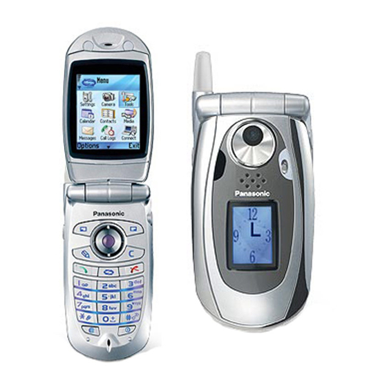
EB-CAX70AU 2.3. Features The Panasonic Phone Model EB-X700 and EB-X701 are high performance, small, light, telephone handsets for business and domestic use on General Packet Radio Service (GPRS) running on GSM networks. The following features are provided: • Triple Band, EGSM 900, GSM 1800 and GSM 1900 operation. -
Page 5: Controls And Indicators
3. OPERATING INSTRUCTIONS 3.1. General This section provides a brief guide to the operation and facilities available on the telephone handset. Refer to the Operating Instructions supplied with the telephone for full operational information. 3.2. Controls and Indicators Left Softkey - Perform action named in lower left of display. - Page 6 - Transfer data between the phone and other devices with an Photolight infrared connection. External Display Accessory Connector and Viewfinder - Plug in most EB-X700 accessories here. Personal Handsfree and TTY Connector - Plug in Personal Handsfree Headset and TTY accessory here. Indicator Light - Remains on during charging. Accessory - Flash to indicate incoming calls.
-
Page 7: Liquid Crystal Displays
3.3. Liquid Crystal Displays The telephone handset has two liquid Crystal Displays - a colour display for main operation and a colour sub-display for a quick review of phone status. Network that phone Phone Status is currently using Time icon area Signal strength Network name Battery charge... -
Page 8: Features Menu Structure
3.5. Features Menu Structure Note that some features are SIM and/or Network dependent. Vodafone Orange Generic Games Games More Games (games under ’Extras’ menu) Micro Golf Micro Golf Balloon Headed Boy Ballon Headed Boy More Games Vodafone live! Orange Menu Vodafone live! Orange World Enter URL... - Page 9 Contacts Address Book Contacts Contacts List (Launches Contacts app) (Launches Contacts app) Create Contact Call Log Speed Dial Settings Settings Settings Profiles Ringtones Ringtones Themes Phone Themes General General Settings …Device ...Phone ...Call ...Device ...Call ...Connection ...Call ...Date & Time ...Date &...
-
Page 10: Imei And Software Identification
3.6. IMEI and Software Identification To check the IMEI number of the phone: Press: * # 0 6 # To identify the software version installed on the phone: Press: * # 9 9 9 9 # within five seconds of switching on. 3.7. - Page 11 3.7.5 Enabling Procedure 1. Press 2. Scroll up / down to select: "SIM" for SIM Personalisation "Network" for Network Personalisation "Sub-Network" for Sub-Network Personalisation "ServiceProvider" for Service Provider Personalisation, or "Corporate" for Company Personalisation. 3. Press 4. Enter the 8 or 16 digit Control Key and press 5.
-
Page 12: Technical Description
TECHNICAL DESCRIPTION 4.1. RF Overview 4.1.1 General Specifications The telephone is a triple band product incorporating three switchable transceivers, GSM 900 (EGSM 900) band, GSM 1800 (DCS 1800) band, and GSM 1900 (PCS 1900) band. The transmit and receive bands are given in the table below: EGSM 900 880-915 MHz 925-960 MHz... -
Page 13: Block Diagram
4.1.3 Block Diagram Figure 4.1: RF Block Diagram 4.1.4 Frequency Plan I, Q output to I, Q output to I, Q output to baseband baseband baseband Rx: 925 - 960 MHz Rx: 1805 - 1880 MHz Rx: 1930 - 1990 MHz 925 - 960 MHz 1805 - 1880 MHz 1930 - 1990 MHz... -
Page 14: Functional Description
4.1.6 Antenna The antenna is a fixed helical type and is designed for a triple band operation (EGSM 900, DCS 1800 and PCS 1900). 4.2. Transmitter 4.2.1 Functional Description Figure 4.3: Transmitter Block Diagram The transceiver IC U500 supports quadrature modulation and employs direct modulation. The differential I/Q inputs from thebaseband circuit are up-converted to the transmit frequency by the quadrature modulator. - Page 15 4.3. Receiver 4.3.1. Functional Description U500 QUAD BAND TRANSCEIVER GSM 850 ANTENNA U502 ANTENNA FL502 BASSBAND SWITCH LOW PASS MODULE FILTER FILTER EGSM 900 FL503 FILTER DCS 1800 FL504 FILTER PCS 1900 Figure 4.4: Receiver Block Diagram The main building block for the receiver is the transceiver IC U500 which includes a direct conversion receiver with in-phase and quadrature demodulation.
-
Page 16: Baseband Overview
The functionality of the GSM Modem is primarily implemented by the Infineon S-Gold ASIC (PMB8870), supported by the Infineon Power Management IC (PMIC) called S/M-Power (PMB86811), with functionality extended by the Panasonic Companion IC (AN32061A). The PMIC and the Companion IC are discussed separately in a later section. - Page 17 EXT_PWR USB I/F VACC UART3 I/O CN USART0 VBUS VDCDC CC1CC4IO PWM_MAIN USART0 DIF_D4 UART3 I/F CC1CC0IO PWM_SUB DIF_D3 IrDA IRDA_SD CC1CC2IO PWM_FLASH SOAKOUT0 VLSD VI NT VBATT Vmain SD/MMC I/F VBATT SD Card SD_SW1 CURRENT BATT_TEMP RF_TEMP FLASH VDD_RTC2 EBU I/F (CS0,CS1) CIC_IRQ...
-
Page 18: Real Time Clock (Rtc)
4.5.2. RF Scheduler and Transmit Power Control S-Gold has a GSM System Interface Block which incorporates in hardware a GSM Timer which is programmed by the Modem software to activate sections of the RF sub-system when required for reception during the paging channel timeslots, and an RF Ramp Controller which additionally switches-on and ramps-up the transmit RF power amplifier when in a voice call sending data packets. - Page 19 4.5.10. Application Processor Clock, Reset & Hand-shaking In the EB-X700 architecture, the Modem is responsible for providing the Application Processor with a 13 MHz clock, and the necessary reset and control handshaking signals. At initial power-up, the Modem (S-Gold) boots itself, while holding the Application Processor in reset.
- Page 20 4.6.2. PCM Audio Routing to/from S-GOLD In the EB-X700 architecture design, the Modem is responsible for providing the Application Processor with a 13 MHz clock, and the necessary reset control handshaking signals. At initial power-up, the Modem (S-Gold) boots itself, while holding the Application Processor in reset.
-
Page 21: Memory Management
4.6.5. Keypad The keypad interface supports up to 6 columns by 5 rows, but only a 5 x 5 keypad matrix is used for EB-X700 design. The keypad scanning algorithm and de-bounce time is software controlled for event detection on both key press and key release. -
Page 22: Bluetooth Module
4.6.6. Bluetooth Module The bluetooth module U201 provides short range (typical 10 meters or less) connectivity from the hanset to bluetooth-enabled devices such as headsets, car kits, and personal computers for transfer of voice and data. The Application processor controls the initialization of the bluetooth module through the UART2 interface (BT-RX, BT-TX, Bt- RTS and BT-CTS) and a reset line (GPIO13) BT-RST controls bluetooth reset. - Page 23 4.6.9. Main LCD Module The main LCD module has 176 x 208 pixels TFT display with 65K colour resolution. The Application processor provides 16-bit interface for RGB pixel data transfer and a 3-wire (LCD-SCL, LCD-SDO and MAINLCD-CS/GPIO12) serial interface (McBSP3) for the module register settings.
-
Page 24: Camera Module
4.6.10. Sub-LCD Module The Sub LCD module has 96x64 pixel CSTN display with 65K colour resolution. The Application processor provides a 3-wire (LCD-SCL, LCD-SDO and SUBLCD-CS/GPIO6) serial interface (McBSP3) for the 16-bit RGB pixel data transfer or the module register settings. The backlighting for the Sub LCD module is provided by +13 V DCDCOUT voltage of Companion IC, which has an on/off function programmed by an I2C link provided by the Modem processor. - Page 25 4.7. Bluetooth Module The X700 handset contains a Bluetooth module centered on Cambridge Silicon Radio’s (CSR) BlueCore3-ROM IC (U201).This provides short range (typically 10 meters or less) connectivity from the handset to Bluetooth-enabled devices such asheadsets, car kits, and personal computers in order to transfer voice and/or data. Shown below is the block diagram of the X700 Bluetooth interface.
- Page 26 The BT chip requires a 26MHz clock that is provided by an internal buffer in the RF Smarti DC+ IC. The buffer receives the 26MHz signal from a VCTCXO and is enabled by BT_CLK_REQ (PIO2). Once the BT IC is powered-up, the BT-CLK-REQ signal will be pulled high by an internal pull-up.
-
Page 27: Power Supplies
4.8. Power Supplies 4.8.1 Introduction The power management block primarily consists of SM-PWR (U304) and Companion IC (U300). U304 is a highly integrated power management ASIC with a complete on/off logic and charging control, regulators, LED drivers, 8-ohm speaker and vibrator driver. -
Page 28: Power Control Logic
4.8.3 Power Control Logic The power on sequence can be initiated when a valid battery voltage is applied (VBATT>3.1). One of following conditions start the Power Up sequence. Power key is pushed for more than 1,000 ms Application of a charger voltage EXT_PWR > 4.0V Real Time Clock alarm generated by U100 (SGOLD) RTCOUT=1 The Power Up sequence is as follows: U304 band gap reference is activated. - Page 29 4.8.4. System Power Supply The following is the summary of the power supplies provided by SM-PWR (U304). Power Supply Description Input Supply Rating 1.80 V ± 0.12 V, 850 mA SDBB Memory core and I/O Supply VMAIN (U102, U203) 1.50 V ± 0.09 V, 170 mA VLBB1 U100 DSP core supply SDBB...
-
Page 30: Battery Charging And Monitoring
Only approved chargers can be used with the handset. By using only approved chargers and the unique Panasonic J300 connector no additional circuitry is provided within the unit to protect from charger voltage exceeding the design limit of 7.0 V. -
Page 31: Esd Handling Precautions
DISASSEMBLY / REASSEMBLY INSTRUCTIONS 5.1. General This section provides disassembly and reassembly procedures for the main components of the phone. These assemblies MUST be performed by qualified service personnel at an authorised service centre. The following Warnings and Cautions MUST be observed during all disassembly / reassembly operations: WARNING The equipment described in this manual contains polarised capacitors utilising liquid electrolyte. - Page 32 5.2. Disassembly 5.2.1. Lower case assembly and main PCB board removal Place thumbs at outer edges of battery cover, press down, then slide the battery cover towards the bottom of the phone. Lift and remove battery, using the tabs at the bottom of the battery. Remove both screw caps located on the top of the phone.
-
Page 33: Main Pcb
Set the phone into the ‘Open’ position. Separate the lower case from the lower cover using a plastic strip (of credit card thickness). Note: When separating the lower case and lower cover the mulitbutton (side key) and headset jack cover will disengage. Note: There are two snaps on both sides of the phone. - Page 34 Turn main PCB over if necessary pivot (1) to release chassis from PCB. Lift up (2) and remove. Release hooks A, B, then C. Caution: Use minimum force to release hooks. The hooks can break or can be easily damaged. Pivot (1), lift (2) and remove sub PCB.
-
Page 35: Keypad Removal
Rotate lower flex lock (2) and remove flex from bottom connector. Remove lower flex from sub PCB. Caution: Lift up (open) or push down (close) flex lock carefully. If damaged, a new connector must be placed on PCB. 5.2.3 Vibrator Removal Gently lift and remove vibrator unit. - Page 36 5.2.5 Microphone and hinge holder removal Lift the microphone insert from its recess on the lower case cover. Using a Trident screwdriver, remove the single screw securing the hinge holder. Retain the screw for reassembly. Gently lift up and remove the hinge holder. Retain for reassembly. 5.2.6.
- Page 37 Separate the upper cover and upper case using a plastic strip (of credit card thickness). Note: There are two snaps on both sides of the phone. Gently press down (1) and slide the flex circuit towards the top of the phone (2). This will remove the flex connection from the brackets.
-
Page 38: Hinge Removal
5.2.7 Hinge Removal Remove hinge. Retain for reassembly. 5.2.8 Receiver, receiver holder and receiver cushion removal Lift and remove the receiver, receiver holder and receiver cushion from its recess in the upper cover. 5.2.9. Camera removal Gently insert a small screwdriver blade or blunt instrument under the camera module, lift up and remove the camera module. - Page 39 5.2.10 Removal of LCD module Gently lift up main LCD connector (1), gently lift up sub LCD connector (2), unplug the DTHF speaker. Gently slide the LCD module to disengage from the two hooks. Caution: Use extreme care when disconnecting sub-LCD connector. Use a straight edge of a plastic strip to gently separate connector in the direction shown.
- Page 40 Remove main LCD module. 5.2.11 RF Antenna, Bluetooth Antenna and SD Cover Removal It is only necessary to remove the antenna if the antenna or antenna contact is damaged. Using a small screwdriver blade or blunt instrument, apply pressure to the antenna snap in the direction shown (1) while pulling the antenna away from the case (2).
- Page 41 5.3. Reassembly CAUTION IF ANY OF THE RF, BLUETOOTH OR BASEBAND SHIELDS ARE REMOVED FROM THE PCB AT ANY TIME, THEY MUST BE REPLACED BY NEW ITEMS. ONCE REMOVED, THE SHIELDS MUST NOT BE REUSED. NOTES: IIf the case assemblies have been disassembled and reassembled more than three times, they should be replaced with new items.
- Page 42 3. Place the main LCD bezel into the opening of the upper cover. 4. Attach the PCB connector into the receiver (1) and (2). Attach the camera connector to the connector on the PCB (3). Caution: Damage to the flex circuit portion of the upper flex PCB is NOT repairable. The flex circuit may be easily stretched or cut during this operation, causing a small tear which can grow with use and render the circuit unusable.
- Page 43 Locate the four screws and torque to 1.3 KGF-CM using a #3ULR0 Trident screwdriver tip. Note: Several parts come with protective sheets. Do not remove. Take care not to let the tabs of a protective sheet get trapped between pieces. Do not let the tabs become attached to any adhesive. 5.3.5 Main LCD and Logo Panel Reassembly Remove the main LCD panel from the liner sheet, and inspect for foreign objects or fingerprints on the interior surface.
- Page 44 5.3.6 Sub LCD Panel Reassembly Remove the panel from the liner sheet, and inspect for foreign objects or fingerprints on the interior surface. If necessary, clean the sub LCD glass surface and the interior of the sub LCD panel with an ionized air spray. Align the panel to the correct orientation, and locate in the upper case.
- Page 45 1) Rotate and align the hinge pivot with the open area facing upward and carefully insert into the main area of the lower cover assembly, taking care to tilt the upper housing assembly without causing damage to the flex circuit during reassembly.
- Page 46 5.3.9 Reassembly of the Main PCB Assembly and SD PCB To be advised. 5.3.10 SD PCB Reassembly SD PCB assembly includes the following: SD flex connector, vibrator unit, SD PCB, chassis. 5.3.11 Main PCB Reassembly Main PCB reassembly includes the following: main PCB, all soldered components, four shield covers, dome sheet and PCB ID label.
-
Page 47: Completing The Assembly
Carefully rotate the SD PCB assembly to the opposite side of the main PCB and align the three tabs. Take care not to damage the SD flex during this step. Press the SD PCB assembly and the main PCB together. Make sure that the two locking hooks properly engage. - Page 48 Reassemble the lower case assembly. Push the antenna in until it locks in position. Place the SD cover into the SD opening and rotate until snapped into place. If necessary replace the I/O cover. Place the headset jack cover in the lower case cover. Assembly the lower case with the lower cover assembly. Close the four snaps making sure that both assemblies are connected.
-
Page 49: Repair Procedures
REPAIR PROCEDURES 6.1. Introduction This section describes the equipment and software required to test and calibrate the phone. Calibration Procedures are described in Section 8. The handset can be connected to a compatible personal computer for electronic adjustment and fault diagnosis. This section provides a description of the equipment required to perform those tasks. -
Page 50: Jigs And Tools
6.4. Jigs and Tools 6.4.1. Personal Computer (PC) The PC (IBM compatible) is used as a Unit Under Test controller. This, in conjunction with the channel box software, allows all of the test facilities normally provided through the keypad of the Unit Under Test. The Microsoft Windows®... -
Page 51: Power Supply
6.4.3. RF Test Jig (Part No. 3WZ001141AAA) The RF Test Jig provides the connections between the test and the phone for unit testing. It also provides power supply for the phone. The following spares item is available for the RF Test Jig. RF Probe (Part No. - Page 52 INTERFACES 7.1.1 External I/O (J300 on main board) External I/O connector is a 14-pin user interface connector that provides external UART, USB, charger and other interface to the X700 handset. Pin No. Signal Function Name Ground SERIAL-UP TXD, UART data transfer to OMAP, or UARTS0-TXD, UART data transfer to S-GOLD SERIAL- RXD, OMAP UART data transfer to EXT, or...
- Page 53 7.1.2 Board to Board Connector (J400 on main board) The board to board connector is a 80-pin inner signal exchanging connector that connects the main board with the upper flex board for main LCD, Sub LCD, camera and other interfaces. The signal names below are based on the signal names on the schematic of the upper flex board.
- Page 54 RGBD1 OMAP pixel data line 1 to Main LCD RGBD2 OMAP pixel data line 2 to Main LCD RGBD3 OMAP pixel data line 3 to Main LCD RGBD4 OMAP pixel data line 4 to Main LCD RGBD5 OMAP pixel data line 5 to Main LCD RGBD6 OMAP pixel data line 6 to Main LCD RGBD7...
- Page 55 VDD-IR Power supply for IrDA module Ground Ground Ground HF-SPK+ Hands free speaker output + HF-SPK- Hands free speaker output - Ground 7.1.3 Main Board to SD/SIM Board Connector (J403 on main board) The main board to SD/SIM board connector is a 25-pin inner signal exchanging connector that connects the main board with the SD/SIM board for SD card, SIM card and other interface signals.
- Page 56 7.1.4 Main LCD Connector (J103 on upper flex board) The main LCD connector is a 40-pin inner signal exchanging connector that connects to the main LCD module on the upper flex board. The signal names below are based on the signal names on the schematic of the upper flex board Pin No.
- Page 57 7.1.5. Sub LCD Connector (J101 on upper flex board) The Sub LCD connector is a 20-pin inner signal exchanging connector that connects to the Sub LCD module on the upper flex board. The signal names below are based on the signal names on the schematic of the upper flex board. Pin No.
- Page 58 7.1.6. Camera Connector (J102 on upper flex board) Pin No. Signal Upper Flex Function Name Camera CAM-I2C- Camera I2C data line CAM-I2C- Camera I2C clock line CAM- Camera external clock from OMAP EXCLK CAM- Camera vertical sync signal from OMAP VSYNC CAM- Camera horizontal sync signal from OMAP...
- Page 59 7.1.7 Mini SD Connector (J102 on SD/SIM board) The Mini SD connector is a 11-pin inner signal exchanging connector that connects to the SD card on the SD/SIM board. The signal names below are based on the signal names on the schematic of the SD/SIM board. Pin No.
- Page 60 7.1.8 SIM Card Connector (J101 on SD/SIM board) The SIM card connector is a 7-pin inner signal exchanging connector that connects to the SIM card on the SD/SIM board. The signal names below are based on the signal names on the schematic of the SD/SIM board. Pin No.
-
Page 61: Fault Finding
FAULT FINDING 8 FAULT FINDING 8.1. RF Waveforms NOTE: The measurements shown below are by FET probe. When using a FET probe, it should be protected by a 10 dB pad. Some of the measurement points are non-50 Ω , therefore signal levels are approximate. Do not probe the output of the Power Amplifier or the Front-end Module's transmit path 2.7V -50.4dBm... - Page 62 FAULT FINDING 1.2V 1.2V 1.2V 1.2V 900 MHz: 0V 1800/1900 MHz: 2.7 Vp-p Square Wave 2.7 Vp-p 2.7V 2.7V Square Wave 2.7V 2.7V ~1.5V 26MHz 26MHz 26MHz 2.7V >500 mVp-p >500 mVp-p ~1Vpp 3 Vp-p 2.7V Square Wave Figure 8.3: Transceiver IC (U500) and VCTCXO (Y500), clock and control signals ~ +3 dBm 2.7V 1800/1900 MHz...
- Page 63 FAULT FINDING ~ +3 dBm 1800/1900 MHz 900 MHz: 0V 31.25 dBm 1800/1900 MHz: 2.7 Vp-p Square Wave 1800/1900 MHz ~ +5 dBm Vsupply (3.8 ~ 4.2 V) 900 MHz 34.25 dBm ~ +3 dBm ~1.4 Vp-p 900 MHz Square Wave 900 MHz 2.7 Vp-p Square Wave...
- Page 64 FAULT FINDING 1.8V BT Ant BT Filter ~-2.5dBm Connector 0dBm Figure 8.7: Bluetooth filter (FL200) 1.8V 2.7V 26MHz 1.8V F = 2441MHz RF Input; Signal level = ~-2dBm Figure 8.8: Bluetooth module (U201) Provisional Issue Section 8 PMCE041201C8 Revision 1 –...
- Page 65 FAULT FINDING 8.2. Baseband Fault Analysis 8.2.1 Major Power-on Fault Analysis On the X700 handset, major power-on fault is defined as the failure of powering up the phone from the major hardware components or software code such as 26MHz system clock failure, S/M power failure, S-GOLD failure, and S-GOLD code corruption.
- Page 66 FAULT FINDING Fault Symptoms Root Cause Debugging Action Code No 26MHz at C504 Bad Y500 or no VRF1 Check pin3 of Y500, replace Y500 if there is voltage no 26MHz clock. Check VRF1/TP335 with Ohm meter, if <100 Ohm, debug the RF section; Otherwise, replace U304, S/M power.
- Page 67 FAULT FINDING 8.2.4 OMAP Controlled Hardware Fault from Initialization Fault Symptoms Root Cause Debugging Action Code No related default voltage Voltage supply shorting; Check VDBB/TP324 (1.8V), V28/ supply to OMAP or bad S/M power IC; or TP330 (2.8V), VBB3/TP342 (1.5V); bad Companion IC If one or more than one of above voltages are not present, use an Ohm...
- Page 68 FAULT FINDING This page is intentionally blank. Provisional Issue Section 8 PMCE041201C8 Revision 1 – 8 – Service Manual...
-
Page 69: Calibration Procedures
9 CALIBRATION PROCEDURES 9.1 Introduction NOTE: For software download instructions, refer to the User Manual supplied with the Dragonfly software. The following procedures MUST be performed after replacement or repair of the PCB. Failure to do so may result in incorrect operation of the telephone. - Page 70 9.2.2 Power Level Tables The following tables show the measurement limits according to power level: EGSM 900 Output Power (dBm) Power Level Target (PL) Nominal 32.25 32.0 32.5 30.5 30.0 31.0 29.0 28.5 29.5 26.5 27.5 24.5 25.5 22.5 23.5 20.5 21.5 18.5...
- Page 71 GSM 1900 Output Power (dBm) Power Level Target (PL) Nominal 29.25 29.0 29.5 27.5 27.0 28.0 26.0 25.5 26.5 24.0 23.5 24.5 22.0 21.5 22.5 20.0 19.5 20.5 18.0 17.5 18.5 16.0 15.5 16.5 14.0 13.5 14.5 12.0 11.5 12.5 10.0 10.5 -0.5...
- Page 72 9.3 Baseband Calibration 9.3.1 System Overview Power Meter Signal Generator PC (with "Dongle") Phone Headset Jack Stabilised Power Supply Voltage : 3.7 V Cable P-test Mode 9.3.2 Press the power key to turn on the mobile phone. Start the PhoneTool program. The following screen is then displayed: 1.
- Page 73 NOTE : If the message "ERROR! No Connection" is displayed, check the cable connections, the power supply and that the phone is switched on. Repeat steps 1 and 2. 3. Select "ptest_mode", and check the log window. >>> "Sending to mobile...OK". The mobile is now in ptest_mode.
-
Page 74: Battery Voltage Ad Calibration
9.3.4 Battery Voltage AD Calibration 1. Click mode button and select "Non signaling test". – 9-6 – PROVISIONAL ISSUE... - Page 75 1. Click the "Non signaling mode" button. 2. Click the Check Connection button. 3. Check the "On" box located on the bottom of the ADC Meas(urement) box. 4. Change the power supply PS-1 voltage from 3.7 V to 4.0 V 5.
- Page 76 9.3.6 Battery Temperature AD Calibration 1. Connect PS-2 so that 1.42V is supplied to TBAT. 2. Monitor the average value of the tbat ADC reading. If this average value is outside the range of 3700 to 3300, then the unit has failed. 3.
- Page 77 9.4 Transmit Power Calibration Note: Before calibrating the mobile, ensure that: The latest version of Panasonic PhoneTool (Version 10.0) is being used. The mobile has been placed in Test Mode. The supply voltage is set to 3.8V with a current limit of 2.5A or higher.
- Page 78 To adjust the DAC to obtain the desired Tx power level: Select the required “Band” and “PA Level,” and click the "Get" button. The default ramping value for the selected band and PA Level will be displayed. Input the Tx ARFCN (see “Calibration Channels” at the end of this section for the input channel), and press Enter key.
- Page 79 Repeat Step 4 (input and set) until the target power level is displayed on the power meter. (Refer to the Calibration Specification tables at the end of this section for target power levels.) Enter the final DAC16 value from Step 5 into the TX Excel spreadsheet. The spreadsheet will automatically calculate the channel compensation value and place it in the appropriate eep memory location on the eep worksheet within the same Excel file.
- Page 80 To calibrate other PA Levels or Bands, repeat Steps 1 through 6. When all channels, power levels, and bands are calibrated, save the Excel sheet of eep data using File -> Save As -> Text (Tab delimited) -> Save. − 9-12 − PROVISIONAL ISSUE...
- Page 81 Proceed to Section 4.0 of this document if nothing else needs to be calibrated. Otherwise, continue with subsequent calibration sequences. − 9-13 − PROVISIONAL ISSUE...
- Page 82 Calibration Channels The following table shows the calibration channels. It is important to perform the calibration at these specific channels, as the software performs linear interpolation based upon these channels. Calibrating Band Segment Channel E-GSM Calibration Limits The following tables provide the target output power levels for calibration. For each power level, the target power is listed in the Nominal column.
-
Page 83: Vctcxo (Frequency) Calibration
9.5 VCTCXO (Frequency) Calibration Note: Before calibrating the mobile, ensure that: The latest version of Panasonic PhoneTool (Version 10.0) is being used. The mobile has been placed in Test Mode. The supply voltage is set to 3.8V with a current limit of 2.5A or higher. - Page 84 To begin calibration of the VCTCXO, select “Non-Signaling Test” from the “Modes” pull-down menu in PhoneTool and complete the following steps: Click the "Non-Signaling Mode" button. Click the “Check Connection” button. Select TSC = 5. (Make sure the call box has the same setting for TSC) Check the “1900 Band”...
- Page 85 12. After the values are downloaded into PhoneTool (this may take a few seconds), double-click the “eep_static” folder in the EEPROM window. 13. Under “eep_static,” select the “rf_adjcomp” folder in the folders list − 9-17 − PROVISIONAL ISSUE...
- Page 86 Rxlev Calibration Note: Before calibrating the mobile, ensure that: The latest version of Panasonic PhoneTool (Version 10.0) is being used. The mobile has been placed in Test Mode. The supply voltage is set to 3.8V with a current limit of 2.5A or higher.
- Page 87 Input the Rx ARFCN (EGSM = 37 ch, DCS = 699 ch, PCS = 661ch) and press the Enter key. NOTE: If the PCS band is being calibrated, the “1900 Band” box must first be checked. Use the pull-down menu to select the Gain "Rx(1) = 69 dB.” Check the "Burst Rx"...
- Page 88 Proceed to Section 4.0 of this document. 9.2.7. Calibration Update Procedure Before proceeding to Step 1 of the calibration update procedure, there are three update scenarios to consider. Tx calibration only – Rename the text file to “falcon_delta00129.007.dep” and place it into the zip file located in the PhoneTool directory named “falcon_eep_cfg_dep.zip.”...
- Page 89 Press the power key to turn on the mobile phone (Assuming the handset is in “Test Mode”). Start the PhoneTool program. Click the "V24 AT# On". Click the “Check Connection” button. From the “Settings” pull-down menu, select “Phone Tool Settings” −...
- Page 90 Check the COM port Setting Set the “PC Baud Rate” to 115200 Select “Read Static Eeprom Values Only” Set “EEPROM & Delta file prefix name” to “falcon” − 9-22 − PROVISIONAL ISSUE...
- Page 91 10. From the “Modes” pull-down menu, select “EEPROM” − 9-23 − PROVISIONAL ISSUE...
- Page 92 11. Click the “UPDATE” button on the toolbar. It will take a few seconds to update the TX and RX calibration values. Click “OK” after the pop-up window that states “EEPROM has been successfully updated”. 12. Tx and Rx calibration update is complete. Put the phone in Normal mode. −...
-
Page 93: Replacement Parts List
10. REPLACEMENT PARTS LIST 10.1. Upper Case REF. NO. PART NO. DESCRIPTION 9ZM027A UPPER BACK COVER ASSY 1GM008A UPPER FRONT COVER ASSY 2EM014A LCD PANEL 4BM002A LCD HOLDER M62 M12 EY80014A MAGNET 9ZM034B HINGE 2RM017A HINGE PIVOT 2RM021A RECIEVER CLIP 6HM022A CUSHION 7GM010AAAA... -
Page 94: Lower Case
KEYPAD CHINA EM14 M1001 BT80062AAA BATTERY PACK (EU) M1002 BT80062ABA BATTERY PACK (CN) EM19 EM07 AN80037A ANTENNA EM18 EM08 EG80453P EB-X700 MAIN PCB EM09 EF80108F LOWER FLEX EM10 4GM004A ANTENNA METAL CONTACT EM16 EM12 AN80034B 3-BAND STUB ANT EM13 EG80465F... -
Page 95: Main Pcb Assembly
10.3. Main PCB Assembly Ref. No. Part No. Part Name & Description Grid Ref. No. Part No. Part Name & Description Grid BT300 N4ECD19A0001 BUTTON BATTERY C221 F1L0J1040002 CERAMIC CAPACITOR 0.1UF 6.3V C100 F1L0J1040002 CERAMIC CAPACITOR 0.1UF 6.3V C222 F1L0J1040002 CERAMIC CAPACITOR 0.1UF 6.3V C101... - Page 96 Ref. No. Part No. Part Name & Description Grid Ref. No. Part No. Part Name & Description Grid C321 ECJ1VB0J225K CERAMIC CAPACITOR 2.2UF 6.3V C504 F1L1C102A027 CERAMIC CAPACITOR 0.001UF 16V C322 F1L1E100A057 CERAMIC CAPACITOR 10PF 25V C506 F1L1E270A057 CERAMIC CAPACITOR 27PF 25V C323 ECJ1VB0J225K...
- Page 97 Ref. No. Part No. Part Name & Description Grid Ref. No. Part No. Part Name & Description Grid D201 B0JCCD000002 DIODE L501 G1C1R0JA0021 INDUCTOR D300 B0JCMD000023 DIODE L502 G1C6N8J00004 COIL 6.8NH D301 B0JCMD000023 DIODE L503 ELJRF4N7JFB INDUCTOR 4.7NH D302 B0JCMD000023 DIODE L505 ELJRF4N7JFB...
- Page 98 Ref. No. Part No. Part Name & Description Grid Ref. No. Part No. Part Name & Description Grid R233 ERJ1GEJ103C FIXED RESISTOR 10K 1/20W R430 ERJ2GEJ330X FIXED RESISTOR 33 1/16W R245 ERJ1GEJ103C FIXED RESISTOR 10K 1/20W R432 ERJ2GEJ330X FIXED RESISTOR 33 1/16W R250 ERJ1GEJ152C...
-
Page 99: Lcd Pcb Assembly
10.4. LCD PCB Assembly 10.5. Mini SD/SIM PCB Assembly Ref. No. Part No. Part Name & Description Grid Ref. No. Part No. Part Name & Description Grid C106 F1G1A104A012 CAPACITOR 0.1UF 10V M1010 AP80048A SD CARD ADAPTOR C107 ECJ0EB0J105M CERAMIC CAPACITOR 1UF 6.3V C113 F1G1H150A565... -
Page 100: Block Diagrams
11. BLOCK DIAGRAMS 11.1. RF Band PMB6258 SMARTI DC+ Tri-band MEC FEM GN06006L 850MHz In A In B In C Drive 900 TX EGSM SAW matc hing DCS SAW matc hing TCXO Ext RF Drive PCS SAW 26 MHz 50 ohm matc hing FSYS_BB... - Page 101 11.2. Baseband EXT-PWR USART0 CONNECTOR UART3 UART3 (TX, RX) IrDA LCD I/F Main LCD 176x208 MCBSP3 SCLK,SDATA TFT Color CAM I/F Sub LCD Reset, CS Color 96x64 CSTN MMC/SD Regulator Nominal Voltages JTAG TEST PADS KEYBL-PWM VLBB1 (S-GOLD DSP) = 1.50V Keypad Camera VLBB2 (S-GOLD Core) = 1.50V...
-
Page 102: Circuit Diagrams
12. CIRCUIT DIAGRAMS 12.1. Main PCB (SGOLD MODEM PROCESSOR SECTION) U100 VINT PMB8870 V1.1BS F12 AB16 I2C-SDA PM-INT USART0-RXD AB17 I2C-SCL I2C-SCL USART0-TXD S-POWER I/F AB18 PM-INT I2C-SDA USART0-RTS AB19 USART0-CTS USART0-TXD R107 USART0-RXD CC2CC510 USB-DPLUS R109 I/O CONNECTOR USART0-CTS 1.5K I2S3-CLK USB-DMINUS... - Page 103 12.2. Main PCB (Board to Board Connector) VMAIN DCDCOUT J400 AXK79308001 C417 SG-CAM-PWM VMAIN IRDA-SD-MODE VMAIN CAM-FLASH PWM-SUB Keypad PWM-MAIN I2C-SDA-CAM I2C-SCL-CAM TP428 TP430 DS400 CAM-STBY LNJ926W8C0MC DS410 OP-DET CAM-RSTZ NOT_MOUNTED LNJ926W8C0MC SH1,2 R405 R409 CAM-LCLK TP500 TP509 OPEN U400 CAM-HS MRSS22L-E DS401...
- Page 104 12.3. Main PCB (Power Management) CIC-IRQ VMAIN VBATT VINT R303 CURRENT USART0-TXD VBUS VACC R304 USART0-RXD R305 USART0-RTS VRTC3 VBB3 SDBB VRTC2 D305 EMZ6.8ET2R VMAIN R307 TP344 TP341 TP342 TP343 USART0-CTS HS-SD USART0-DTR-PAON STOUTRPRE VMEM HS-SD TP321 TP302 TP306 TP310 TP304 TP308 STINR...
- Page 105 TP217 TP220 TP221 TP222 VRF3 VBT18 12.4. Main PCB (Baseband) PCM-OUT PCM-IN U201 PCM-CLK BC313143A05-IRK-E4 TP212 BT-CLK-REQ TP211 SH3,5 TP210 BT26M VDD-USB USB-DP TP209 VDD-PI USB-DN VDD-PADS VDD-MEM SPI-CSB C209 VDD-MEM SPI-CLK 0.01U VDD-MEM SPI-MOSI VBT18 C281 VDD-MEM SPI-MISO VDD-MEM 2.2U VDD-MEM UART-TX...
- Page 106 12.5. Main PCB (RF Band) VRF1 U503 L520 R516 RF3146PTR13 27NH VCC1 VCC3-GSM VCC1-GSM VCC3-DCS/PCS VCC2-GSM VCC2-DCS/PCS VCC-OUT VCC-OUT DCS/PCS-IN VBATT FL506 BAND-SEL DCS/PCS-OUT EXCML16A270U TX-ENABLE VBATT VBATT R539 VRAMP GSM-OUT GSM-IN NC-GND VRF1 NC-GND GSM-IS-GND C526 FL500 GND1-GSM BGH181B GND-BASE OUT1 TX2X...
- Page 107 12.6. Mini SD/SIM PCB – 12-6 – PROVISIONAL ISSUE...
- Page 108 12.7. Mini SD/SIM PCB Flex Tall P100 P101 AXK8L24125 AXK8L24125 – 12-7 – PROVISIONAL ISSUE...
- Page 109 12.8. LCD PCB – 12-8 – PROVISIONAL ISSUE...
-
Page 110: Layout Diagrams
13. LAYOUT DIAGRAMS 13.1. Main PCB (Top View) – 13-1 – PROVISIONAL ISSUE... - Page 111 13.2. Main PCB (Bottom View) 1.5K 1.5K – 13-2 – PROVISIONAL ISSUE...
- Page 112 13.3. LCD PCB (Bottom View) – 13-3 – PROVISIONAL ISSUE...
- Page 113 13.4. Mini SD/SIM PCB S100 EVQP7D01K D100 MA2S111000L [Top View] [Bottom View] R100 J100 K1MN25B00067 FF0225SS1-R3000 – 13-4 – PROVISIONAL ISSUE...