Table of Contents
Quick Links
SERVICE MANUAL
U.S. and foreign patents licensed form Dolby Laboratories
Licensing Corporation.
MICROFILM
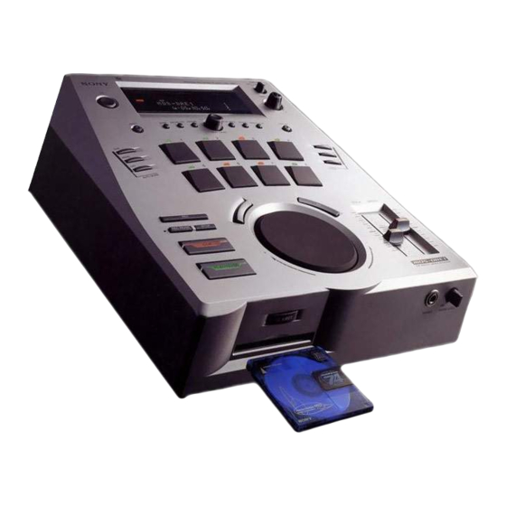
MDS-DRE1
Model Name Using Similar Mechanism
MD Mechanism Type
Base Unit Name
Optical Pick-up Name
SPECIFICATIONS
MINIDISC RECORDER/PLAYER
US Model
Canadian Model
AEP Model
UK Model
MDS-JA3ES
MDM-2CR
MBU-2B
KMS-210A/J-N
– Continued on next page –
Table of Contents

Related Manuals for Sony MDS-DRE1


Summary of Contents for Sony MDS-DRE1
- Page 1 MDS-DRE1 SERVICE MANUAL US Model Canadian Model AEP Model UK Model Model Name Using Similar Mechanism MDS-JA3ES U.S. and foreign patents licensed form Dolby Laboratories Licensing Corporation. MD Mechanism Type MDM-2CR Base Unit Name MBU-2B Optical Pick-up Name KMS-210A/J-N SPECIFICATIONS –...
-
Page 2: Table Of Contents
OPERATION. REPLACE THESE COMPONENTS WITH DE FONCTIONNEMENT. NE REMPLACER CES COM- SONY PARTS WHOSE PART NUMBERS APPEAR AS POSANTS QUE PAR DES PIÈCES SONY DONT LES SHOWN IN THIS MANUAL OR IN SUPPLEMENTS PUB- NUMÉROS SONT DONNÉS DANS CE MANUEL OU LISHED BY SONY. -
Page 3: Servicing Notes
SECTION 1 SERVICING NOTES SAFETY CHECK-OUT CAUTION After correcting the original service problem, perform the follow- Danger of explosion if battery is incorrectly replaced. ing safety check before releasing the set to the customer: Replace only with the same or equivalent type recommended by Check the antenna terminals, metal trim, “metallized”... - Page 4 CAUTION Use of controls or adjustments or performance of procedures other than those specified herein may result in hazardous ra- diation exposure. This appliance is classified as a CLASS 1 LASER product. The CLASS 1 LASER PRODUCT MARKING is located on the rear exterior.
- Page 5 FORCED RESET The system microprocessor can be reset in the following way. Use these methods when the unit cannot be operated normally due to the overrunning of the microprocessor, etc. Method 1: Method 2: Set TP (RESET) of the DIGITAL board to ground momentarily. Disconnect the power plug, and short-circuit CN451 of the POWER board with a pair of tweezers, etc.
- Page 6 Reading the Retry Cause Display Higher Bits Lower Bits Hexa- Hexadecimal Cause of Retry Occurring conditions decimal b7 b6 b5 b4 b3 b2 b1 b0 Binary shock *1 When more than 3.5 shocks are detected When ADER was counted more than ader5 five times continuously Discontinuous address...
- Page 7 NAMES AND FUNCTIONS OF PARTS...
-
Page 9: Disassembly
SECTION 3 DISASSEMBLY Note: Follow the disassembly procedure in the numerical order given. UPPER CABINET SECTION 4 two connectors (CN801, 802) 6 upper cabinet section 4 two connectors (CN701, 751) 3 Open the upper cabinet section in arrow direction. 2 two screws ×... - Page 10 BRACKET (MD) 1 Rotate the pully (BD) in arrow direction A and move the slider assembly in arrow direction B . 2 two screws (B2.6 × 18) 2 two screws (B2.6 × 18) 3 two collars 3 two collars slider assembly 4 insulator (MD) 4 insulator (MD)
- Page 11 BASE UNIT AND LOADING MOTOR ASSEMBLY 3 belt 4 two screws (B2.6 × 5) 1 screw (BV3 × 6) 6 loading motor assembly 5 connector (CN192) 2 base unit 1 two screws (BV3 × 6) SLIDER ASSEMBLY MOUNTING 3 Move the slider assembly in arrow direction B , and lock it to the lever (SLM).
-
Page 12: Test Mode
SECTION 4 TEST MODE 4-1. Setting the Test Mode [ ] [AMS] Press (POWER) switch while pressing the knob to turn POWER ON. 4-2. Exiting the Test Mode [REPEAT] Press the button. Unplug the power plug from an outlet. 4-3. Basic Operations of the Test Mode [AMS] [ENTER/YES] [EDIT/NO]... - Page 13 4-4-2. Operating the Continuous Recording Mode 1. Entering the continuous recording mode 1 Set the MO disc in the unit. 2 Rotate the [AMS] knob and display “CREC MODE”. 3 Press the [ENTER/YES] button to change the display to “CREC IN”. 4 When access completes, the display changes to “CREC ( ”...
- Page 14 4-6. Test Mode Displays [DISPLAY] Each time the button is pressed, the display changes in the following order. MODE display n Error rate display n Address display 1. MODE display Displays “TEMP ADJUS”, “CPLAY MODE”, etc. 2. Error rate display Error rates are displayed as follows.
-
Page 15: Electrical Adjustments
SECTION 5 ELECTRICAL ADJUSTMENTS Precautions for Checking Laser Diode Emission Precautions for Adjustments To check the emission of the laser diode during adjustments, never 1) When replacing the following parts, perform the adjustments and checks with ® in the order shown in the following table. view directly from the top as this may lose your eye-sight. - Page 16 Laser Power Adjustment Temperature Compensation Offset Adjustment Connection: Save the temperature data at that time in the non-volatile memory as 25 ˚C reference data. Laser power Note: meter 1. Usually, do not perform this adjustment. 2. Perform this adjustment in an ambient temperature of 22 ˚C to 28 ˚C. Perform it immediately after the power is turned on when the internal temperature of the unit is the same as the ambient temperature.
- Page 17 [AMS] Traverse Adjustment 11. Rotate the knob until the waveform of the oscilloscope moves closer to the specified value. In this adjustment, waveform varies at intervals of approx. 3%. Connection: Adjust the waveform so that the specified value is satisfied as Oscilloscope much as possible.
- Page 18 Focus Bias Adjustment Error Rate Check CD Error Rate Check Adjusting Method: 1. Load a continuously recorded disc (Refer to “Page 15 Creat- Checking Method: ing Continuously Recorded Disc”). 1. Load a check disc (MD) TDYS-1. [AMS] [AMS] 2. Rotate the knob and display “CPLAY MODE”.
- Page 19 Adjusting Points and Connecting Points [BD Board] (Side A) D101 IC191 [BD Board] (Side B) TP58 (IOP) TP57 (I + 5V) IC101 RV101 TP31 (VC) IC171 RV102 TP75 (TEO) IC121 – 19 –...
-
Page 20: Diagrams
MDS-DRE1 SECTION 6 DIAGRAMS SCTX (Page 23) 6-1. BLOCK DIAGRAM – SERVO Section – DIGITAL SIGNAL PROCESSOR, DODT DODT EFM/ACIRC ENCODER/DECODER (Page 23) PEAK IC121 (1/2) OVER WRITE DETECT EFMO DIDT HEAD DRIVE REGISTER DIGITAL MODULATOR IC181, Q181, 182 AUDIO... -
Page 21: Block Diagram - Main Section (1/2)
MDS-DRE1 6-2. BLOCK DIAGRAM – MAIN Section (1/2) – (Page 25) DIDT 40 34 IC151 SDTO SHOCK PROOF MEMORY CONTROLLER, (1/4) ATRAC ENCODER DODT IC501 (Page 25) DODT (Page 22) DIDT DATA DODT SELECTOR DOUT LATCH FINB LRCK LRCK IC153 (1/2) -
Page 22: Block Diagram - Main Section (2/2)
MDS-DRE1 6-3. BLOCK DIAGRAM – MAIN Section (2/2) – DIGITAL AUDIO SAMPLING RATE CONVERTER INTERFACE RECEIVER IC451 IC401 J601 DIDT DATAO DATAI DATA OUT DIN1 (Page 24) COAXIAL IN SAMPLING DATA INPUT BCKO DIN2 WAVE RATE DEMODULATOR INTERFACE LRCKO LRCK... -
Page 23: Block Diagram - Display/Key/Power Supply Section
MDS-DRE1 6-4. BLOCK DIAGRAM – DISPLAY/KEY/POWER SUPPLY Section – (Page 25) FLUORESCENT FL DRIVER CONTROL, KEY CONTROL, LED DRIVE FL DRIVER INDICATOR TUBE IC201 IC101 FL101 J851 FOOT SW FSW1 REC/PAUSE SWDT SDATA +5V/+7V REGULATOR SCLK IC411 MD SERVO SECTION B+... -
Page 24: Notes For Printed Wiring Board And Schematic Diagram
MDS-DRE1 • Circuit Boards Location 6-5. NOTES FOR PRINTED WIRING BOARD AND SCHEMATIC DIAGRAM (In addition to this, the necessary note is printed in each block) Note on Schematic Diagram: Note on Printed Wiring Board: • X : parts extracted from the component side. -
Page 25: Printed Wiring Board – Bd Board (Side A)
MDS-DRE1 6-6. PRINTED WIRING BOARD – BD Board (SIDE A) – • See page 29 for Circuit Boards Location. • Semiconductor Location Ref. No. Location D101 D181 D183 IC191 Q181 Q182 – 31 – – 32 –... -
Page 26: Printed Wiring Board – Bd Board (Side B)
MDS-DRE1 6-7. PRINTED WIRING BOARD – BD Board (SIDE B) – • See page 29 for Circuit Boards Location. • Semiconductor Location Ref. No. Location D155 D161 IC101 IC102 IC121 IC122 IC151 IC171 IC172 IC181 IC182 Q101 Q151 Q162 Q163... -
Page 27: Schematic Diagram - Bd Section (1/2)
MDS-DRE1 6-8. SCHEMATIC DIAGRAM – BD Section (1/2) – • See page 67 for Waveforms. • See page 70 for IC Block Diagrams. (Page 37) The components identified by mark ! or dotted Les composants identifiés par une marque ! sont line with mark ! are critical for safety. -
Page 28: Schematic Diagram - Bd Section (2/2)
MDS-DRE1 6-9. SCHEMATIC DIAGRAM – BD Section (2/2) – • See page 67 for Waveforms. • See page 70 for IC Block Diagrams. (Page 47) (Page 36) (Page 47) – 37 – – 38 –... -
Page 29: Printed Wiring Boards - Detection Sw Board, Motor Board
MDS-DRE1 6-10. PRINTED WIRING BOARDS – DETECTION SW Board, MOTOR Board – • See page 29 for Circuit Boards Location. DETECTION SW BOARD MOTOR BOARD CN193 (Page 40) (Page 39) CN192 C199 S191 (PLAY POSITION) – CN191 S192 (PACK OUT) -
Page 30: Schematic Diagram - Detection Sw/Motor Section
MDS-DRE1 6-11. SCHEMATIC DIAGRAM – DETECTION SW/MOTOR Section – (Page 47) – 41 – – 42 –... -
Page 31: Printed Wiring Board – Digital Board (Side A)
MDS-DRE1 6-12. PRINTED WIRING BOARD – DIGITAL Board (SIDE A) – • See page 29 for Circuit Boards Location. • Semiconductor (Page 63) (Page 63) Location Ref. No. Location D101 IC101 IC201 IC251 IC252 (RESET) IC253 F-10 IC254 H-10 IC255... -
Page 32: Printed Wiring Board – Digital Board (Side B)
MDS-DRE1 6-13. PRINTED WIRING BOARD – DIGITAL Board (SIDE B) – • See page 29 for Circuit Boards Location. • Semiconductor Location Ref. No. Location D311 D312 IC151 IC152 IC153 IC154 IC202 IC256 H-10 IC257 G-10 IC258 IC259 IC260 I-10... -
Page 33: Schematic Diagram - Digital Section (1/4)
MDS-DRE1 6-14. SCHEMATIC DIAGRAM – DIGITAL Section (1/4) – • See page 68 for Waveforms. • See page 71 for IC Block Diagrams. (Page (Page (Page 49) (Page (Page 51) – 47 – – 48 –... -
Page 34: Schematic Diagram - Digital Section (2/4)
MDS-DRE1 6-15. SCHEMATIC DIAGRAM – DIGITAL Section (2/4) – • See page 68 for Waveforms. • See page 71 for IC Block Diagrams. (Page (Page 65) (Page 53) – 49 – – 50 –... -
Page 35: Schematic Diagram - Digital Section (3/4)
MDS-DRE1 6-16. SCHEMATIC DIAGRAM – DIGITAL Section (3/4) – • See page 68 for Waveforms. • See page 71 for IC Block Diagrams. (Page 47) (Page 53) – 51 – – 52 –... -
Page 36: Schematic Diagram – Digital Section (4/4)
MDS-DRE1 6-17. SCHEMATIC DIAGRAMS – DIGITAL Section (4/4) – • See page 68 for Waveforms. • See page 71 for IC Block Diagrams. (Page 49) (Page 65) (Page – 53 – – 54 –... -
Page 37: Printed Wiring Board - Panel Section (1)
MDS-DRE1 6-18. PRINTED WIRING BOARD – PANEL Section (1) – • See page 29 for Circuit Boards Location. • Semiconductor Location Ref. No. Location D101 D102 IC201 IC421 IC431 (Page 63) (Page 60) (Page 59) (Page 60) – 55 –... -
Page 38: Schematic Diagram - Panel Section (1)
MDS-DRE1 6-19. SCHEMATIC DIAGRAM – PANEL Section (1) – • See page 69 for Waveform. • See page 75 for IC Block Diagram. (Page 61) (Page 61) (Page 62) (Page 65) – 57 – – 58 –... -
Page 39: Printed Wiring Boards - Panel Section (2)
MDS-DRE1 6-20. PRINTED WIRING BOARDS – PANEL Section (2) – • See page 29 for Circuit Boards Location. • Semiconductor Location – JOG Board– Ref. No. Location (Page 60) D361 D362 D363 D364 D365 D366 D371 PH381 PH382 Q361 Q362... -
Page 40: Schematic Diagram - Panel Section (2)
MDS-DRE1 6-21. SCHEMATIC DIAGRAM – PANEL Section (2) – • See page 76 for IC Block Diagram. (Page (Page (Page 66) (Page 58) (Page 65) – 61 – – 62 –... -
Page 41: Printed Wiring Boards – Power Section
MDS-DRE1 6-22. PRINTED WIRING BOARDS – POWER Section – • See page 29 for Circuit Boards Location. (Page 56) (Page 44) (Page 60) • Semiconductor Location – POWER Board– Ref. No. Location D201 D202 D203 D204 (Page 60) D205 D206... -
Page 42: Schematic Diagram - Power Section
MDS-DRE1 6-23. SCHEMATIC DIAGRAM – POWER Section – • See page 70 for IC Block Diagrams. (Page 62) (Page 54) (Page 61) (Page 50) (Page 57) The components identified by mark ! or dotted Les composants identifiés par une marque ! sont line with mark ! are critical for safety. - Page 43 • Waveforms – BD Board – – DIGITAL Board – 1 IC101 $¶, $• (I, J) (Play mode) 6 IC121 $¢ (XPLCK) !¡ IC121 #∞ (XTAI) 1 IC501 (º (LRCK), IC601(º (LRCK) 6 IC451 #™ (LRCKO), IC501 $¢ (ALRCK) !¡ IC451 !£ (XI), IC751 !£ (XI) IC751 #™...
- Page 44 – CENTER Board – 1 IC201 !£ (XOUT) 5 Vp-p 10 MHz – 69 –...
- Page 45 • IC Block Diagrams – BD Board – IC121 CXD2535CR 74 73 72 71 69 68 67 66 65 63 62 61 60 58 57 56 55 54 53 52 51 50 DVSS DIN PLL DIPO 34 MHz (22 MHz) SE 76 ANALOG MUX COMP...
- Page 46 IC151 MPC17A38VMEL DRIVER DRIVER DRIVER DRIVER DC/DC CONVERTER PRE-DRIVER PRE-DRIVER PRE-DRIVER PRE-DRIVER CLOCK CONTROL CONTROL CONTROL CONTROL DETECTOR – DIGITAL Board – IC152, 153 SN74HC125ANS IC202, 258 SN74HC74ANS 13 12 11 14 VCC 1 OE 4 OE 1 2 3 4 5 6 2 OE 3 OE...
- Page 47 IC301 AK4520A-VF-E2 IC256, 257 SN74HC595ANS ∆Σ 8× CLOCK MODULATOR INTERPOLATOR DIVIDER ∆Σ 8× MODULATOR INTERPOLATOR SHIFT REGISTER COMMON SERIAL I/O VOLTAGE INTERFACE ∆Σ DECIMATION MODULATOR FILTER ∆Σ DECIMATION LATCH MODULATOR FILTER 9 10 PARALLEL DATA OUTPUT IC311 CXA8054M IC401 LC89051V-TLM TST2 TEST TST1...
- Page 48 IC451, 751 CXD8517Q 31 30 29 28 TEST MUTE DEMP FIR FILTER CONTROL COEFFIENT OUTPUT I/F (P1-S0) (RAM/ROM/A XLAT R-CH RAM B L-CH RAM B ATT/MODE SWDT FIS1 SAMPLING REGISTER REGISTER REGISTER FIS0 RATE POINTER GENERATOR REGISTER PASS 20 bit ADD 19 bit 19 bit 20 bit ADD...
- Page 49 IC501, 601 CXD2537R SWDT SCLK ATRAC Encoder/Decoder XLAT SRDT SENS SMD0 SMD1 Memory Data Controller I/F Memory XINT RCPB XRAS WRMN ATRAC Encoder/Decoder I/F TST0 XCAS TST1 DI Block TST2 RAM R/W Controller XRST CD-ROM Encoder/Decoder TST3 TST4 Clock Generator TST5 –...
- Page 50 IC801 CXD2720Q 79 – 71 70 69 68 – 54 X768 128K BIT CLOCK GENERATOR/ BFOT DELAY RAM TIMING CIRCUIT VDD1 INVI VSS3 AVS5 AO2P DAC2 AO2N LRCK SERIAL DAC1 XMST DATA VSS7 INTERFACE AVD5 ADC1 AVD2 AIN2 ADC2 AVS2 VDD3 XVSS ADC3...
-
Page 51: Power Board
– DISPLAY Board – – POWER Board – IC101 M66004M8FP IC401, 411 BA3963 DIG11 MODE1(5V) DIG12 DIGITAL OUTPUT DIG0 DIG15 CIRCUIT MODE2(7V) INDICATION – CONTROLLER SERIAL RECEIVE OVER CIRCUIT DATA CURRENT PROTECT INDICATION RESET OUTPUT CONTROL PORT RESISTOR (2BIT) REF. V CLOCK CODE/COMMAND XOUT... -
Page 52: Ic Pin Function Description
6-24. IC PIN FUNCTION DESCRIPTION • BD BOARD IC101 CXA1981AR (RF AMP, FOCUS/TRACKING ERROR AMP) Pin No. Pin Name Function Middle point voltage (+2.5V) generation output terminal 2 to 7 A to F Signal input from the optical pick-up detector Operational input for the F signal Operational output for the F signal Light amount monitor input from the optical pick-up block laser diode... - Page 53 • BD BOARD IC121 CXD2535CR (DIGITAL SIGNAL PROCESSOR, DIGITAL SERVO PROCESSOR, EFM/ACIRC ENCODER/DECODER Pin No. Pin Name Function FS256 Clock signal (11.2896 MHz) output terminal (MCLK system) Not used (open) Focus OK signal output to the system controller (IC101) “H” is output when focus is on (“L”: NG) DFCT Defect on/off selection signal output terminal Not used SHCK...
- Page 54 Pin No. Pin Name Function MCLK MCLK clock signal (22.5792 MHz) output terminal Not used (open) Invert output of the BCK (pin #™) Not used (open) XBCK DVDD0 — Power supply terminal (+5V) (digital system) WDCK Word clock signal (88.2 kHz) output terminal (MCLK system) Not used (open) RFCK Read frame clock signal (7.35 kHz) output terminal (MCLK system) Not used (open) Write frame clock signal (7.35 kHz) output terminal (EFM decoder PLL system when playback...
- Page 55 Pin No. Pin Name Function I (A) Tracking error signal input from the CXA1981AR (IC101) AUX2 I (A) Auxiliary signal input terminal Not used (fixed at “L”) DCHG I (A) Connected to the ground I (A) Error signal input for the laser automatic power control Not used (fixed at “L”) TEST1 Input terminal for the test (fixed at “L”) ADIP duplex FM signal (22.05 kHz ±...
- Page 56 • CENTER BOARD IC201 M30612M8A-404FP (FLUORESCENT INDICATOR TUBE DRIVE CONTROLLER, KEY CONTROLLER, LED DRIVER) Pin No. Pin Name Function FSW0 Foot switch (PLAY/PAUSE) input terminal FSW1 Foot switch (REC/PAUSE) input terminal 3, 4 — Not used (open) — Not used (fixed at “H”) REM-CON Not used (fixed at “H”) —...
- Page 57 Pin No. Pin Name Function LED2-G LED2-O LED3-G LED3-O LED4-G LED4-O LED5-G LED drive signal output of the pad indicator “L”: LED on LED5-O LED6-G LED6-O LED7-G LED7-O LED8-G LED8-O 81 to 86 — Not used (fixed at “H”) INPUT-SEL1 INPUT switch (S601) input terminal “L”: optical input, “H”: analog/coaxial input INPUT-SEL0 INPUT switch (S601) input terminal “L”: analog input, “H”: optical/coaxial input...
- Page 58 • DIGITAL BOARD IC101 M30610MC-TTX1057M (SYSTEM CONTROLLER) Pin No. Pin Name Function 1, 2 TEST Not used (pull up) 3, 4 TEST Not used (fixed at “H”) Subcode Q sync (SCOR) input from the CXD2535CR (IC121) SQSY “L” is input every 13.3 msec Almost all, “H” is input —...
- Page 59 Pin No. Pin Name Function READY-KEY Ready status input from the CXD2720Q (IC801) XS24-KEY Not used (pull up) RST-37 Reset signal output to the ATRAC encoder (IC501) and ATRAC decoder (IC601) “L”: reset Reset signal output to the CXA1981AR (IC101), CXD2535CR (IC121), MPC17A38VMEL RST-DIG (IC151), A/D, D/A converter (IC301), digital audio interface receiver (IC401), sampling rate converter (IC451, 751) and CXD2720Q (IC801) “L”: reset...
- Page 60 Pin No. Pin Name Function Laser power select signal output to the CXD2535CR (IC121) and HF module switch circuit WPOWER “L”: playback mode, “H”: recording mode SDA-CDSP Two-way data bus with the DSP (IC701) SND-CDSP Not used (open) Two-way data bus with the EEPROM (IC171) Serial clock signal output to the EEPROM (IC171) and DSP (IC701) SENSE Internal status monitor input from the CXD2535CR (IC121)
- Page 61 • DIGITAL BOARD IC701 DSP56004FJ66 (DSP) Pin No. Pin Name Function GNDA — Ground terminal (for EMI control output buffer) MCS0 Chip select signal output terminal Not used (open) 3 to 5 MA15 to MA13 Address signal output terminal Not used (open) VCCA —...
- Page 62 Pin No. Pin Name Function SDI0 Playback serial data input from the CXD2537R (IC601) Debug serial data output terminal Not used (pull up) DSI/OS0 Debug serial data input terminal Not used (fixed at “L”) DSCK/OS1 Debug serial clock signal in/out terminal Not used (fixed at “L”) Debug request signal input terminal Not used (fixed at “H”) 62 to 65 MD7 to MD4...
-
Page 63: Exploded Views
SECTION 7 EXPLODED VIEWS NOTE: • -XX and -X mean standardized parts, so they • Items marked “*” are not stocked since they The components identified by mark ! or dotted line with mark may have some difference from the original are seldom required for routine service. - Page 64 (2) UPPER SIDE CABINET SECTION supplied supplied with S601 supplied with RV701 supplied not supplied Ref. No. Part No. Description Remark Ref. No. Part No. Description Remark 4-210-109-01 BUTTON (EJECT) 4-950-189-51 KNOB (A) (VOL) * 52 A-4724-210-A EJECT BOARD, COMPLETE * 63 A-4724-207-A REC BOARD, COMPLETE X-4950-070-1 BUTTON (PLAY) ASSY...
- Page 65 (3) LOWER SIDE CABINET SECTION M801 MDM-2CR supplied T901 supplied supplied supplied The components identified by Les composants identifiés par une mark ! or dotted line with marque ! sont critiques pour la mark ! are critical for safety. sécurité. Replace only with part num- Ne les remplacer que par une pièce ber specified.
- Page 66 (4) MECHANISM DECK SECTION (MDM-2CR) supplied supplied M191 MBU-2B not supplied not supplied Ref. No. Part No. Description Remark Ref. No. Part No. Description Remark 4-967-673-01 SPRING, COMPRESSION 4-983-110-01 CUSHION (LVO) 4-967-671-01 INSULATOR (MD) A-4672-071-B HOLDER ASSY, COMPLETE 4-970-710-01 SPRING, COMPRESSION X-4947-136-2 HOLDER ASSY 4-979-400-01 LEVER (DOOR) 4-967-646-01 SPRING (SHT), TORSION...
- Page 67 (5) BASE UNIT SECTION (MBU-2B) S102 HR901 M102 M101 The components identified by Les composants identifiés par une mark ! or dotted line with marque ! sont critiques pour la mark ! are critical for safety. sécurité. Replace only with part num- Ne les remplacer que par une pièce ber specified.
- Page 68 SECTION 8 ELECTRICAL PARTS LIST NOTE: • Due to standardization, replacements in the • Items marked “*” are not stocked since they The components identified by mark ! or dotted line with mark parts list may be different from the parts speci- are seldom required for routine service.
- Page 69 CENTER Ref. No. Part No. Description Remark Ref. No. Part No. Description Remark IC121 8-752-378-79 IC CXD2535CR R132 1-216-097-00 RES, CHIP 100K 1/10W IC122 8-759-243-19 IC TC7SU04F R133 1-216-129-00 METAL CHIP 2.2M 1/10W IC151 8-759-179-60 IC MPC17A38VMEL R134 1-216-037-00 METAL CHIP 1/10W IC171 8-759-504-12 IC X24C01S...
- Page 70 CENTER DETECTION SW Ref. No. Part No. Description Remark Ref. No. Part No. Description Remark C206 1-162-282-31 CERAMIC 100PF R371 1-249-421-11 CARBON 2.2K 1/4W C207 1-164-159-11 CERAMIC 0.1uF R372 1-247-843-11 CARBON 3.3K 1/4W C208 1-104-396-11 ELECT 10uF R373 1-249-425-11 CARBON 4.7K 1/4W C209...
- Page 71 DIGITAL Ref. No. Part No. Description Remark Ref. No. Part No. Description Remark A-4724-211-A DIGITAL BOARD, COMPLETE (US, Canadian) C318 1-126-395-11 ELECT 22uF A-4724-215-A DIGITAL BOARD, COMPLETE (AEP, UK) C319 1-163-125-00 CERAMIC CHIP 220PF *********************** C320 1-163-125-00 CERAMIC CHIP 220PF <...
- Page 72 DIGITAL Ref. No. Part No. Description Remark Ref. No. Part No. Description Remark C802 1-163-251-11 CERAMIC CHIP 100PF IC259 8-759-232-74 IC TC74HC163AF C803 1-163-038-00 CERAMIC CHIP 0.1uF IC260 8-759-232-74 IC TC74HC163AF C804 1-163-038-00 CERAMIC CHIP 0.1uF IC271 8-759-927-72 IC TL1591CP C805 1-163-038-00 CERAMIC CHIP 0.1uF...
- Page 73 DIGITAL DISPLAY Ref. No. Part No. Description Remark Ref. No. Part No. Description Remark R302 1-216-017-00 RES, CHIP 1/10W R901 1-216-295-00 SHORT R303 1-216-017-00 RES, CHIP 1/10W R304 1-216-017-00 RES, CHIP 1/10W < CONPOSITION CIRCUIT BLOCK > R311 1-216-057-00 METAL CHIP 2.2K 1/10W RB101...
- Page 74 DISPLAY EJECT FADER Ref. No. Part No. Description Remark Ref. No. Part No. Description Remark < FLUORESCENT INDICATOR TUBE > C384 1-124-589-11 ELECT 47uF FL101 1-517-776-11 INDICATOR TUBE, FLUORESCENT < CONNECTOR > < IC > CN205 1-784-641-11 CONNECTOR, BOARD TO BOARD 11P CN207 1-506-481-11 PIN, CONNECTOR 2P IC101...
- Page 75 MOTOR POWER Ref. No. Part No. Description Remark Ref. No. Part No. Description Remark 1-653-412-11 MOTOR BOARD C604 1-164-159-11 CERAMIC 0.1uF C605 1-164-159-11 CERAMIC 0.1uF ************ C606 1-126-933-11 ELECT 100uF < CAPACITOR > C607 1-164-159-11 CERAMIC 0.1uF C199 1-164-159-11 CERAMIC 0.1uF C701 1-130-467-00 MYLAR...
- Page 76 POWER Ref. No. Part No. Description Remark Ref. No. Part No. Description Remark IC422 8-759-604-32 IC M5F7810 A-4724-208-A PSW BOARD, COMPLETE IC431 8-759-917-18 IC SN74HCU04AN ******************** IC451 8-759-327-15 IC M62005L IC501 8-759-633-42 IC M5293L < CONNECTOR > IC601 8-759-430-27 IC GP1F37R (DIGITAL OPTICAL IN) CN801 1-564-321-00 PIN, CONNECTOR 2P IC602...
- Page 77 MDS-DRE1 Ref. No. Part No. Description Remark Ref. No. Part No. Description Remark 7-685-903-31 SCREW +PTPWH 3X10 (TYPE2) 7-685-876-09 SCREW +BVTT 3X16 (S) 7-682-961-01 SCREW +PSW 4X8 7-685-247-19 SCREW +KTP 3X10 TYPE2 NON-SLIT 7-685-645-79 SCREW +BVTP 3X6 TYPE2 N-S 7-621-775-20 SCREW +B 2.6X5 7-685-902-11 SCREW +PWH 2.6X6...