beautypg.com
Manuals
Brands
Hitachi Manuals
Storage
Travelstar HTS542525K9SA00
Hitachi Travelstar HTS542525K9SA00 Manuals
Manuals and User Guides for Hitachi Travelstar HTS542525K9SA00. We have
4
Hitachi Travelstar HTS542525K9SA00 manuals available for free PDF download: Specifications, Quick Installation Manual, Datasheet
Hitachi Travelstar HTS542525K9SA00 Specifications (298 pages)
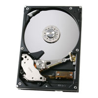
3.5 inch hard disk drive
Brand:
Hitachi
| Category:
Storage
| Size: 1.57 MB
Table of Contents
Table of Contents
5
General
15
Introduction
15
References
15
Abbreviations
15
Caution
17
General Features of the Drive
19
Fixed-Disk Subsystem Description
23
Control Electronics
23
Head Disk Assembly
23
Actuator
23
Drive Characteristics
25
Default Logical Drive Parameters
25
Table 1: Formatted Capacities
25
Data Sheet
26
World Wide Name Assignment
26
Drive Organization
26
Drive Format
26
Table 2: Mechanical Positioning Performance
26
Table 3: Word Wide Name Assignment
26
Cylinder Allocation
27
Performance Characteristics
29
Command Overhead
29
Mechanical Positioning
29
Table 4: Command Overhead
29
Table 5: Mechanical Positioning Performance
29
Table 6: Full Stroke Seek Time
30
Table 7: Single Track Seek Time
30
Drive Ready Time
31
Operating Modes
31
Table 8: Latency Time
31
Table 9: Drive Ready Time
31
Table 10: Description of Operating Modes
31
Table 11: Mode Transition Times
32
Mode Transition Time
32
Defect Flagging Strategy
33
Table 12: PATA Plist Physical Format
33
Electrical Interface Specification
35
Connector Location
35
Pin DC Power Connector
36
AT Signal Connector
36
Signal Definitions (PATA Model)
37
Table 13: Signal Definitions
37
Signal Descriptions
38
Table 14: Special Signal Definitions for Ultra DMA
38
Interface Logic Signal Levels (Pata Model)
41
Signal Definition (SATA Model)
41
Tx+ / Tx
41
Rx+ / Rx
42
Out of Band Signaling (SATA Model)
42
Reset Timings
43
Table 15: System Reset Timing Chart
43
Table 16: System Reset Timing
43
PIO Timings
44
Write DRQ Interval Time
44
Read DRQ Interval Time
44
Table 17: PIO Cycle Timings Chart
44
Multi-Word DMA Timings
45
Table 18: Multiword DMA Cycle Timing Chart
45
Table 19: Multiword DMA Cycle Timings
45
Ultra DMA Timings
46
Initiating Read DMA
46
Table 20: Ultra DMA Cycle Timings (Initiating Read)
46
Host Pausing Read DMA
47
Table 21: Ultra DMA Cycle Timing Chart (Host Pausing Read)
47
Table 22: Ultra DMA Cycle Timings (Host Pausing Read)
47
Host Terminating Read DMA
48
Table 23: Ultra DMA Cycle Timing Chart (Host Pausing Read)
48
Table 24: Ultra DMA Cycle Timings (Host Pausing Read)
48
Device Terminating Read DMA
49
Table 25: Ultra DMA Cycle Timing Chart (Host Pausing Read)
49
Table 26: Ultra DMA Cycle Timings (Device Terminating Read)
49
Initiating Write DMA
50
Table 27: Ultra DMA Cycle Timing Chart (Initiating Write)
50
Device Pausing Write DMA
51
Table 28: Ultra DMA Cycle Timing Chart (Device Pausing Write)
51
Table 29: Ultra DMA Cycle Timings (Device Pausing Write)
51
Device Terminating Write DMA
52
Table 30: Ultra DMA Cycle Timing Chart (Device Terminating Write)
52
Table 31: Ultra DMA Cycle Timings (Device Terminatingwrite)
52
Host Terminating Write DMA
53
Table 32: Ultra DMA Cycle Timing Chart (Host Terminating Write)
53
Table 33: Ultra DMA Cycle Timings (Host Terminating Write)
53
Addressing of Registers
54
Cabling
54
Table 34: I/O Address Map
54
Specification
57
Jumper Settings
57
Jumper Pin Location
57
Jumper Pin Identification
57
Jumper Pin Assignment
58
Jumper Positions
59
Logical Head Default
60
Table 35: Jumper Positions for Capacity Clip to 32GB
61
Table 36: Jumper Settings for Disabling Auto Spin
61
Environment
63
Temperature and Humidity
63
Table 37: Temperature and Humidity
63
Corrosion Test
64
DC Power Requirements
64
Table 38: Limits of Temperature and Humidity
64
Input Voltage
65
Table 39: Input Voltage
65
Power Supply Current (Typical)
66
Table 40: Power Supply Current of 80GB and 160GB Models
66
Power Supply Generated Ripple at Drive Power Connector
67
Table 41: Power Supply Generated Ripple at Drive Power Connector
67
Reliability
68
Data Integrity
68
Cable Noise Interference
68
Start/Stop Cycles
68
Preventive Maintenance
68
Data Reliability
68
Required Power-Off Sequence
68
Mechanical Specifications
69
Physical Dimensions and Weight
69
Mounting Hole Locations
70
Connector Locations
71
Drive Mounting
72
Heads Unload and Actuator Lock
72
Vibration and Shock
73
Operating Vibration
73
Nonoperating Vibration
73
Table 42: Random Vibration PSD
73
Table 43: Random Vibration PSD Profile Break Points (Operating)
73
Random Vibration
73
Operating Shock
74
Nonoperating Shock
74
Nonoperating Rotational Shock
74
Acoustics
75
Identification Labels
75
Safety
76
UL and CSA Approval
76
German Safety Mark
76
Flammability
76
Safe Handling
76
Environment
76
Secondary Circuit Protection
76
Electromagnetic Compatibility
77
CE Mark
77
C-TICK Mark
77
BSMI Mark
77
MIC Mark
77
Packaging
77
Substance Restriction Requirements
77
General
79
Introduction
79
Terminology
79
Deviations from Standard
79
Registers
81
Register Set
81
Alternate Status Register
82
Command Register
82
Cylinder High Register
82
Cylinder Low Register
82
Data Register
83
Device Control Register
83
Drive Address Register
84
Device/Head Register
84
Error Register
85
Features Register
85
Sector Count Register
85
Sector Number Register
86
Status Register
86
General Operation
89
Reset Response
89
Register Initialization
90
Diagnostic and Reset Considerations
91
Sector Addressing Mode
92
Logical CHS Addressing Mode
92
LBA Addressing Mode
92
Power Management Features
93
Power Mode
93
Power Management Commands
93
Standby Timer
93
Interface Capability for Power Modes
94
Function
95
Attributes
95
Attribute Values
95
Attribute Thresholds
95
Threshold Exceeded Condition
95
Commands
95
Off-Line Read Scanning
95
Error Log
96
Self-Test
96
Security Mode Feature Set
97
Security Mode
97
Security Level
97
Passwords
98
Operation Example
98
Command Table
102
Host Protected Area Feature
104
Example for Operation (in LBA Mode)
104
Security Extensions
105
Seek Overlap
106
Write Cache Function
107
Reassign Function
108
Auto Reassign Function
108
Nonrecovered Write Errors
108
Power-Up in Standby Feature Set
109
Advanced Power Management Feature Set (APM)
110
Automatic Acoustic Management Feature Set (AAM)
111
Address Offset Feature
112
Enable/Disable Address Offset Mode
112
Identify Device Data
113
Exceptions in Address Offset Mode
113
48-Bit Address Feature Set
114
Streaming Feature Set
114
Streaming Commands
115
Urgent Bit
115
Flush to Disk Bit
115
Not Sequential Bit
115
Read Continuous Bit
116
Write Continuous Bit
116
Handle Streaming Error Bit
116
Streaming Logs
116
SATA bist (Built-In Self Test)
116
SATA Interface Power Management
116
Software Setting Preservation
116
COMRESET Preservation Requirements
117
SATA II Optional Features
118
Asynchronous Signal Recovery
118
Device Power Connector Pin 11 Definition
118
Phy Event Counters
118
READ LOG EXT Log Page 11H
120
Counter Definitions
120
Identifier 000H
120
Identifier 001H
120
SCT Command Transport Feature Set
121
SCT Command Protocol
122
SCT Command Set
130
Command Protocol
141
PIO Data in Commands
141
PIO Data out Commands
142
Non-Data Commands
144
DMA Commands
145
Command Descriptions
147
Check Power Mode (E5H/98H)
152
Configure Stream (51H)
153
Device Configuration Overlay (B1H)
155
DEVICE CONFIGURATION RESTORE (Subcommand C0H)
155
DEVICE CONFIGURATION FREEZE LOCK (Subcommand C1H)
155
DEVICE CONFIGURATION IDENTIFY (Subcommand C2H)
156
DEVICE CONFIGURATION SET (Subcommand C3H)
156
Download Microcode (92H)
159
Execute Device Diagnostic (90H)
161
Flush Cache (E7H)
162
Flush Cache Ext (Eah)
163
Format Track (50H)
164
Format Unit (F7H)
166
Identify Device (Ech)
167
Table 84: Identify Device Information
168
Table 85: Identify Device Information
170
Table 86: Identify Device Information
172
Table 87: Identify Device Information
173
Table 88: Identify Device Information
174
Idle (E3H/97H)
178
Idle Immediate (E1H/95H)
179
Table 90: Idle Immediate Command (E1H/95H)
179
Initialize Device Parameters (91H)
180
Table 91: Initialize Device Parameters Command (91H)
180
Read Buffer (E4H)
181
Table 92: Read Buffer (E4H)
181
Read DMA (C8H/C9H)
182
Table 93: Read DMA Command (C8H/C9H)
182
Read DMA Ext (25H)
184
Table 94: Read DMA Ext Command (25H)
184
Read Log Ext (2Fh)
186
Table 95: Read Log Ext Command (2Fh)
186
Table 96: Log Address Definition
187
General Purpose Log Directory
188
Table 97: General Purpose Log Directory
188
Extended Comprehensive SMART Error Log
189
Table 98: Extended Comprehensive SMART Error Log
189
Table 99: Extended Error Log Data Structure
189
Table 100: Command Data Structure
190
Table 101: Error Data Structure
190
Extended Self-Test Log Sector
191
Read Stream Error Log
192
Table 102: Read Stream Error Log
192
Table 103: Stream Error Log Entry
194
Write Stream Error Log
194
Streaming Performance Log
195
Table 104: Write Stream Error Log
195
Table 105: Streaming Performance Parameters Log
196
Table 106: Sector Time Array Entry (Linearly Interpolated)
196
Table 107: Access Time Array Entry (Linearly Interpolated)
196
Read Long (22H/23H)
197
Table 108: Read Long (22H/23H)
197
Read Multiple (C4H)
199
Table 109: Read Multiple (C4H)
199
Read Multiple Ext (29H)
200
Table 110: Read DMA Ext Command (25H)
200
Read Native Max ADDRESS (F8H)
202
Table 111: Read Native Max ADDRESS (F8H)
202
Read Native Max Address Ext (27H)
203
Table 112: Read Native Max Address Ext Command (27H)
203
Read Sectors (20H/21H)
204
Table 113: Read Sectors Command (20H/21H)
204
Read Sector(S) Ext (24H)
206
Table 114: Read Sector(S) Ext Command (24H)
206
Read Stream DMA (2Ah)
208
Table 115: Read Stream DMA Command (2Ah)
208
Read Stream PIO (2Bh)
212
Table 116: Read Stream PIO (2Bh)
212
Read Verify Sectors (40H/41H)
215
Table 117: Read Verify Sectors (40H/41H)
215
Read Verify Sectors Ext (42H)
217
Table 118: Read Verify Sectors Ext Command (42H)
217
Recalibrate (1Xh)
219
Table 119: Recalibrate (1Xh)
219
Security Disable Password (F6H)
220
Table 120: Security Disable Password (F6H)
220
Table 121: Password Information for Security Disable Password Command
220
Security Erase Prepare
221
Table 122: Security Disable Password (F3H)
221
Security Erase Unit (F4H)
222
Table 123: Security Erase Unit (F4H)
222
Table 124: Erase Unit Information
222
Security Freeze Lock (F5H)
224
Table 125: Security Freeze Lock Command (F5H)
224
Security Set Password (F1H)
225
Table 126: Security Set Password Command (F1H)
225
Table 127: Security Set Password Information
225
Security Unlock (F2H)
227
Table 128: Security Unlock Command (F2H)
227
Seek (7Xh)
229
Table 129: Seek Command (7Xh)
229
Set Features (Efh)
230
Table 130: Set Features Command (Efh)
230
Advanced Power Management
231
Set Transfer Mode
231
Write Cache
231
Automatic Acoustic Management
233
Set Max ADDRESS (F9H)
234
Table 131: Set Max ADDRESS Command (F9H)
234
Set Max Set Password (Feature=01H)
236
Table 132: Set Max Set Password Command
236
Table 133: Set Max Set Password Data Contents
236
Set Max Lock (Feature=02H)
237
Table 134: Set Max Lock Command
237
Set Max Unlock (Feature = 03H)
238
Table 135: Set Max Unlock Command (F9H)
238
Set Max Freeze Lock (Feature = 04H)
239
Table 136: Set Max Freeze Lock (F9H)
239
Set Max Address Ext (37H)
240
Table 137: Set Max Address Ext Command (37H)
240
Set Multiple (C6H)
242
Table 138: Set Multiple Command (C6H)
242
Sleep (E6H/99H)
243
Table 139: Sleep Command (E6H/99H)
243
Function Set (B0H)
244
Table 140: S.M.A.R.T. Function Set Command (B0H)
244
Function Subcommands
245
Device Attribute Data Structure
249
Table 141: Device Attribute Data Structure
249
Table 142: Individual Attribute Data Structure
249
Device Attribute Thresholds Data Structure
252
Table 143: Device Attribute Thresholds Data Structure
253
Table 144: Individual Threshold Data Structure
253
Log Directory
254
Summary Error Log Sector
254
Table 145: S.M.A.R.T. Log Directory
254
Table 146: S.M.A.R.T. Summary Error Log Sector
254
Table 147: Error Log Data Structure
255
Table 148: Command Data Structure
255
Table 149: Error Data Structure
255
Self-Test Log Data Structure
256
Table 150: Self-Test Log Data Structure
256
Selective Self-Test Log Data Structure
257
Error Reporting
258
Table 151: Selective Self-Test Log Data Structure
258
Table 152: S.M.A.R.T. Error Codes
258
Standby (E2H/96H)
260
Table 153: Standby (E2H/96H)
260
Standby Immediate (E0H/94H)
262
Table 154: Standby Immediate (E0H/94H)
262
Write Buffer (E8H)
263
Table 155: Write Buffer (E8H)
263
Write DMA (Cah/Cbh)
264
Table 156: Write DMA (Cah/Cbh)
264
Write DMA Ext (35H)
266
Table 157: Write DMA Ext Command (35H)
266
Write DMA FUA Ext (3Dh)
268
Write Log Ext (3Fh)
270
Table 158: Write Log Ext Command (3Fh)
270
Write Long (32H/33H)
271
Table 159: Write Long (32H/33H)
271
Write Multiple (C5H)
273
Table 160: Write Multiple (C5H)
273
Write Multiple Ext (39H)
275
Table 161: Writemultiple Ext Command (39H)
275
Writer Multiple FUA Ext (Ceh)
277
Write Sectors (30H/31H)
279
Table 162: Write Sectors Command (30H/31H)
279
Write Sector(S) Ext (34H)
281
Table 163: Write Sectors Ext
281
Write Stream DMA (3Ah)
283
Table 164: Write Stream DMA Command (3Ah)
283
Write Stream PIO (3Bh)
285
Table 165: Write Stream PIO Command (3Bh)
285
Timings
289
Hitachi Travelstar HTS542525K9SA00 Specifications (171 pages)
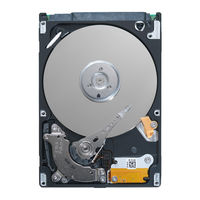
2.5 inch SATA hard disk drive
Brand:
Hitachi
| Category:
Storage
| Size: 2.58 MB
Table of Contents
Table of Contents
3
1 Introduction
8
Abbreviations
8
General
8
Drive Handling Precautions
11
General Caution
11
References
11
2 Outline of the Drive
12
Part 1 Functional Specification
13
3 Fixed Disk Subsystem Description
14
Control Electronics
14
Head Disk Assembly Data
14
4 Fixed Disk Characteristics
15
Formatted Capacity by Model Number
15
Table 1. Formatted Capacity by Model Number
15
Data Sheet
16
Cylinder Allocation
16
Table 2. Data Sheet
16
Table 3. Cylinder Allocation
16
Performance Characteristics
17
Table 4. Performance Characteristics
17
Table 5. Mechanical Positioning Performance
18
Table 6. Full Stroke Seek Time
18
Table 7. Single Track Seek Time
18
Table 8. Latency Time
18
Table 9. Drive Ready Time
19
Table 10. Operating Mode
20
Table 11. Drive Ready Time
20
5 Data Integrity
21
Data Loss on Power off
21
Write Cache
21
Equipment Status
21
WRITE Safety
21
Data Buffer Test
22
Error Recovery
22
Automatic Reallocation
22
Ecc
23
6 Specification
24
Environment
24
Figure 1. Limits of Temperature and Humidity
24
Table 12. Environmental Condition
24
Table 13. Magnetic Flux Density Limits
25
DC Power Requirements
26
Table 14. DC Power Requirements
26
Table 15. Power Consumption Efficiency
27
Reliability
28
Preventive Maintenance
29
Mechanical Specifications
31
Figure 2. Mounting Hole Locations
31
Table 16. Physical Dimensions and Weight
31
Mounting Orientation
32
Vibration and Shock
33
Table 17. Random Vibration PSD Profile Breakpoints (Operating)
33
Table 18. Swept Sine Vibration
33
Table 19. Random Vibration PSD Profile Breakpoints (Nonoperating)
34
Table 20. Operating Shock
34
Table 21. Nonoperating Shock
34
Acoustics
35
Table 22. Weighted Sound Power
35
Identification Labels
36
Electromagnetic Compatibility
36
Safety
37
Packaging
37
Substance Restriction Requirements
37
7 Electrical Interface Specifications
38
Cabling
38
Interface Connector
38
Figure 3. Interface Connector Pin Assignments
38
Signal Definitions
39
Table 23. Interface Connector Pins and I/O Signals
39
Figure 4. Parameter Descriptions
40
Part 2 Interface Specification
41
8 General
42
Introduction
42
Terminology
42
9 Deviations from Standard
43
10 Physical Interface
43
11 Registers
43
Register Naming Convention
44
Command Register
44
Device Control Register
44
Table 24 Register Naming Convention and Correspondence
44
Table 25 Device Control Register
44
Device Register
45
Error Register
45
Features Register
45
LBA High Register
45
Table 26 Device Register
45
Table 27 Error Register
45
LBA Low Register
46
LBA MID Register
46
Sector Count Register
46
Status Register
46
Table 28 Status Register
46
12 General Operation Descriptions
48
Reset Response
48
Table 29 Reset Response Table
48
Diagnostic and Reset Considerations
49
Table 30 Default Register Values
49
Table 31 Diagnostic Codes
49
Table 32 Reset Error Register Values
49
Power-Off Considerations
50
Table 33 Device's Behavior by ATA Commands
50
Sector Addressing Mode
51
Power Management Feature
51
Table 34 Power Conditions
52
Advanced Power Management (Adaptive Battery Life Extender 3) Feature
53
Interface Power Management Mode (Slumber and Partial)
54
Function
54
Security Mode Feature Set
55
Security Level
56
Master Password Revision Code
56
Operation Example
56
Figure 5 Initial Setting
57
Figure 6 Usual Operation
58
Figure 7 Password Lost
59
Table 35 Command Table for Device Lock Operation
60
Protected Area Function
61
Table 36 Command Table for Device Lock Operation - Continued
61
Figure 8 Set Max Security Mode Transition
63
Table 37 Set Max Set Password Data Content
63
Seek Overlap
64
Write Cache Function
64
Reassign Function
64
Figure 9 Seek Overlap
64
48-Bit Address Feature Set
65
Software Setting Preservation Feature Set
66
Native Command Queuing
67
SMART Command Transport (SCT)
67
Table 38 Preserved Software Setting
67
Table 39 SCT Action Code Supported
68
13 Command Protocol
69
Data in Commands
69
Data out Commands
69
Non-Data Commands
70
DMA Data Transfer Commands
71
First-Parity DMA Commands
71
14 Command Descriptions
72
Table 40 Command Set
72
Table 41 Command Set - Continued
73
Table 42 Command Set (Subcommand)
74
Check Power Mode (E5H/98H)
76
Table 43 Check Power Mode Command (E5H/98H)
76
Device Configuration Overlay (B1H)
77
Table 44 Device Configuration Overlay Command (B1H)
77
Table 45 Device Configuration Overlay Features Register Values
77
Table 46 Device Configuration Overlay Data Structure
79
Table 47 DCO Error Information Definition
80
Execute Device Diagnostic (90H)
81
Table 48 Execute Device Diagnostic Command (90H)
81
Flush Cache (E7H)
82
Table 49 Flush Cache Command (E7H)
82
Flush Cache Ext (Eah)
83
Table 50 Flush Cache EXT Command (Eah)
83
Format Track (50H: Vendor Specific)
84
Table 51 Format Track Command (50H)
84
Format Unit (F7H: Vendor Specific)
85
Table 52 Format Unit Command (F7H)
85
Identify Device (Ech)
86
Table 53 Identify Device Command (Ech)
86
Table 54 Identify Device Information
87
Table 55 Identify Device Information
88
Table 56 Identify Device Information
89
Table 57 Identify Device Information
90
Table 58 Identify Device Information
91
Table 59 Identify Device Information
92
Table 60 Identify Device Information
93
Table 61 Identify Device Information
94
Table 62 Identify Device Information
95
Table 63 Number of Cylinders/Heads/Sectors by Models for HTS5425XXK9SA00 / HTS5425XXK9A300
96
Idle (E3H/97H)
97
Table 64 Idle Command (E3H/97H)
97
Idle Immediate (E1H/95H)
98
Table 65 Idle Immediate Command (E1H/95H)
98
Initialize Device Parameters (91H)
99
Table 66 Initialize Device Parameters Command (91H)
99
Read Buffer (E4H)
100
Table 67 Read Buffer Command (E4H)
100
Read DMA(C8H/C9H)
101
Table 68 Read DMA Command (C8H/C9H)
101
Read DMA Ext (25H)
102
Table 69 Read DMA Ext Command (25H)
102
Read FPDMA Queued (60H)
103
Table 70 Read FPDMA Queued Command (60H)
103
Read Log Ext(2Fh)
104
Table 71 Read Log Ext Command (2Fh)
104
Table 72 Log Address Definition
104
Table 73 General Purpose Log Directory
105
Table 74 Extended Comprehensive SMART Error Log
106
Table 75 Extended Error Log Data Structure
106
Table 76 Command Data Structure
107
Table 77 Error Data Structure
107
Table 78 Extended Self-Test Log Data Structure
108
Table 79 Extended Self-Test Log Descriptor Entry
109
Table 80 Command Error Information
109
Table 81 Phy Event Counter Identifier
110
Table 82 Phy Event Counter Information
111
Read Multiple (C4H)
112
Table 83 Read Multiple Command (C4H)
112
Read Multiple Ext (29H)
113
Table 84 Read Multiple Ext Command (29H)
113
Read Native Max Address (F8H)
114
Table 85 Read Native Max Address Command (F8H)
114
Read Native Max Address Ext (27H)
115
Table 86 Read Native Max Address Ext Command (29H)
115
Read Sector(S) (20H/21H)
116
Table 87 Read Sector(S) Command (20H/21H)
116
Read Sector(S) Ext (24H)
117
Table 88 Read Sector(S) Ext Command (24H)
117
Read Verify Sector(S) (40H/41H)
118
Table 89 Read Verify Sector(S) Command (40H/41H)
118
Read Verify Sector(S) Ext (42H)
119
Table 90 Read Verify Sector(S) Ext Command (42H)
119
Recalibrate (1Xh)
120
Table 91 Recalibrate Command (1Xh)
120
Security Disable Password (F6H)
121
Table 92 Security Disable Password Command (F6H)
121
Table 93 Password Information for Security Disable Password Command
121
Security Erase Prepare (F3H)
122
Table 94 Security Erase Prepare Command (F3H)
122
Security Erase Unit (F4H)
123
Table 95 Security Erase Unit Command (F4H)
123
Table 96 Erase Unit Information
123
Security Freeze Lock (F5H)
125
Table 97 Security Freeze Lock Command (F5H)
125
Security Set Password (F1H)
126
Table 98 Security Set Password Command (F1H)
126
Table 99 Security Set Password Information
126
Security Unlock (F2H)
128
Table 100 Security Unlock Command (F2H)
128
Table 101 Security Unlock Information
128
Seek (7Xh)
129
Table 102 Seek Command (7Xh)
129
Sense Condition (F0H : Vendor Specific)
130
Table 103 Sense Condition Command (F0H)
130
Set Features (Efh)
131
Table 104 Set Features Command (Efh)
131
Set Max Address (F9H)
133
Table 105 Set Max Address Command (F9H)
133
Set Max Address Ext (37H)
135
Table 106 Set Max Address Ext Command (37H)
135
Set Multiple (C6H)
137
Table 107 Set Multiple Command (C6H)
137
Sleep (E6H/99H)
138
Table 108 Sleep Command (E6H/99H)
138
Function Set (B0H)
139
Table 109 S.M.A.R.T. Function Set Command (B0H)
139
Figure 10 Selective Self-Test Test Span Example
141
Table 110 Log Sector Addresses
142
Table 111 Device Attribute Data Structure
144
Table 112 Individual Attribute Data Structure
145
Table 113 Status Flag Definitions
146
Table 114 Device Attribute Thresholds Data Structure
148
Table 115 Individual Threshold Data Structure
149
Table 116 SMART Log Directory
149
Table 117 S.M.A.R.T. Error Log Sector
150
Table 118 Error Log Data Structure
150
Table 119 Command Data Structure
151
Table 120 Error Data Structure
151
Table 121 Self-Test Log Data Structure
152
Table 122 Selective Self-Test Log Data Structure
153
Table 123 S.M.A.R.T. Error Codes
153
Standby (E2H/96H)
154
Table 124 Standby Command (E2H/96H)
154
Standby Immediate (E0H/94H)
155
Table 125 Standby Immediate Command (E0H/94H)
155
Table 126 Write Buffer Command (E8H)
156
Write Buffer (E8H)
156
Table 127 Write DMA Command (Cah/Cbh)
157
Write DMA (Cah/Cbh)
157
Table 128 Write DMA Ext Command (35H)
158
Write DMA Ext (35H)
158
Table 129 Write DMA FUA Ext Command (3Dh)
159
Write DMA FUA Ext (3Dh)
159
Table 130 Write FPDMA Queued Command (61H)
160
Write FPDMA Queued (61H)
160
Table 131 Write Log Ext Command
161
Write Log Ext (3Fh)
161
Table 132 Write Multiple Command (C5H)
162
Write Multiple (C5H)
162
Table 133 Write Multiple Ext Command (39H)
163
Write Multiple Ext (39H)
163
Table 134 Write Multiple FUA Ext Command (Ceh)
164
Write Multiple FUA Ext (Ceh)
164
Table 135 Write Sector(S) Command (30H/31H)
165
Write Sector(S) (30H/31H)
165
Table 136 Write Sector(S) Ext Command (34H)
166
Write Sector(S) Ext (34H)
166
Table 137 Write Uncorrectable Ext Command (45H)
167
Write Uncorrectable Ext (45H)
167
Table 138 Timeout Values
169
Timing
169
Hitachi Travelstar HTS542525K9SA00 Quick Installation Manual (5 pages)
Hitachi Travelstar 5K250: Install Guide
Brand:
Hitachi
| Category:
Storage
| Size: 0.17 MB
Hitachi Travelstar HTS542525K9SA00 Datasheet (2 pages)
2.5-INCH HARD DISK DRIVES
Brand:
Hitachi
| Category:
Storage
| Size: 0.25 MB
Related Products
Hitachi Travelstar HTS542516K9SA00
Hitachi 2.5-INCH Travelstar HTS542525K9A300
Hitachi Travelstar HTS542516K9A300
Hitachi Travelstar HTS542512K9A300
Hitachi Travelstar HTS542580K9A300
Hitachi Travelstar HTS542512K9SA00
Hitachi Travelstar HTS542580K9SA00
Hitachi HTS543212L9A300
Hitachi HTS541680J9SA00 - Travelstar 80 GB Hard Drive
Hitachi Travelstar HTS541060G9SA00
Hitachi Categories
Projector
Air Conditioner
Drill
Power Tool
TV
More Hitachi Manuals