Yamaha EMX512SC Service Manual
Powered mixer
Hide thumbs
Also See for EMX512SC:
- Owner's manual (36 pages) ,
- Manuel du propriétaire (36 pages) ,
- Brochure & specs (6 pages)
Table of Contents
Quick Links
このサービ スマニ ュ アルはエ コ パルプ
(ECF : 無塩素系漂白パルプ) を使用 し ています。
This document is printed on chlorine free (ECF) paper.
PA
011791
EMX512SC: 200510-99750
EMX312SC: 200510-78750
RK512: 200510-5250
POWERED MIXER
SERVICE MANUAL
EMX512SC
■
CONTENTS
SPECIFICATIONS ( 総合仕様 ) .......................................................3/5
Panel Layout ( パネルレ イ アウ ト )...............................................7
CIRCUIT BOARD LAYOUT ( ユニ ッ ト レ イ アウ ト ) ........................10
Wiring Diagram( 基板結線図 ) ....................................................11
Dimensions ( 寸法図 ) ...................................................................13
Disassembly Procedures ( 分解手順 ) ..................................14
Lsi Pin Description (LSI 端子機能表 ) .......................................24
Ic Block Diagram (IC ブ ロ ッ ク 図 ) ............................................26
Circuit Boards ( シー ト 基板図 ) ................................................28
Inspection( 検査 ) ...................................................................50/58
PS CIRCUIT BOARD REPAIR GUIDE
(PS シー ト 故障修理ガ イ ド )........................................................66/76
PARTS LIST
BLOCK & LEVEL DIAGRAM( ブ ロ ッ ク & レ ベルダ イ アグ ラ ム )
CIRCUIT DIAGRAM( 回路図 )
Copyright (c) Yamaha Corporation. All rights reserved. PDF–K4902
EMX312SC
• OPTION
RK512 RACK MOUNT KIT ( ラ ッ ク マウ ン ト キ ッ ト )
HAMAMATSU, JAPAN
'05.09
Table of Contents

Related Manuals for Yamaha EMX512SC


Summary of Contents for Yamaha EMX512SC
- Page 1 このサービ スマニ ュ アルはエ コ パルプ (ECF : 無塩素系漂白パルプ) を使用 し ています。 CIRCUIT DIAGRAM( 回路図 ) This document is printed on chlorine free (ECF) paper. 011791 EMX512SC: 200510-99750 HAMAMATSU, JAPAN EMX312SC: 200510-78750 Copyright (c) Yamaha Corporation. All rights reserved. PDF–K4902 ’05.09 RK512: 200510-5250...
-
Page 2: Important Notice
IMPORTANT NOTICE This manual has been provided for the use of authorized Yamaha Retailers and their service personnel. It has been assumed that basic service procedures inherent to the industry, and more specifically Yamaha Products, are already known and understood by the users, and have therefore not been restated. -
Page 3: Specifications
EMX512SC/EMX312SC ■ SPECIFICATIONS • General Specifications Output Conditioins U, V H, B, W, K, O UNIT 4 Ω Maximum Output Power SPEAKERS OUT EMX512SC Both ch drive, 1 kHz, 8 Ω THD+N ≤ 0.5% 4 Ω EMX312SC 8 Ω Input... -
Page 4: Input Characteristics
Connector Impedance Normal Norminal Max. before Clip 0.1 Ω 4 Ω Speakers SPEAKERS EMX512SC 125 W 500 W [A1, B1] SPEAKON [A1, A2, B1, B2] EMX312SC 75 W 300 W [A2, B2] Phone Jack 600 Ω MAIN OUT [L, R] 10 kΩ... - Page 5 EMX512SC/EMX312SC ■ • 出力 条件 最小 標準 最大 単位 4 Ω 最大出力 SPEAKERS OUT EMX512SC A/B 両チ ャ ン ネル駆動 , 8 Ω 1kHz, THD+N ≦ 0.5% 4 Ω EMX312SC 8 Ω 入力 出力 条件 最小 標準 最大 単位 周波数特性...
- Page 6 ノ ミ ナルレ ベル 最大 ノ ン ク リ ッ プ レ ベル 0.1 Ω 4 Ω Speakers SPEAKERS EMX512SC 125 W 500 W [A1, B1] ス ピ コ ン端子 [A1, A2, B1, B2] EMX312SC 75 W 300 W [A2, B2] フ ォ ーン端子...
-
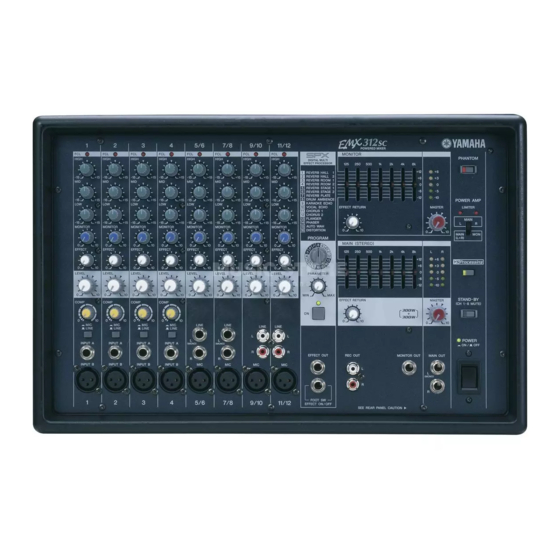
Page 7: Panel Layout
EMX512SC/EMX312SC ■ PANEL LAYOUT • Controls on Each channel • Digital Effect Section 1 FCL (Feedback Channel Locating) indicator 0 PROGRAM selector 2 Equalizer gain control (HIGH, MID, and LOW) q PARAMETER control 3 MONITOR control w DIGITAL EFFECT ON switch... - Page 8 EMX512SC/EMX312SC • MAIN Section MAIN • MONITOR Section MONITOR t Graphic Equalizer faders a Graphic Equalizer faders y EFFECT RETURN control s EFFECT RETURN control u MASTER control d MASTER control i LEVEL meters f LEVEL meters o MAIN OUT L and R jacks...
- Page 9 EMX512SC/EMX312SC • POWER Section POWER h PHANTOM switch j LIMITER indicators k POWER AMP switch l YS Processing switch ; STAND-BY switch z POWER switch and indicator h PHANTOM ス イ ッ チ j LIMITER イ ン ジケー タ ー...
-
Page 10: Circuit Board Layout
EMX512SC/EMX312SC ■ CIRCUIT BOARD LAYOUT • Rear View • Top View JACK • Front View • Side View JACK... -
Page 11: Wiring Diagram
(3P) (3P) (3P) (3P) (3P) CN401 CN302 CN402 (13P) (5P) (7P) CN001 CN002 CN101 CN102 CN201 CN202 (3P) (3P) (3P) (3P) (3P) (3P) indicates that connectors are connected directly to circuit boards. CN402 CN401 (5P) (7P) JACK EMX512SC only EMX512SC... - Page 12 OUT-CN301 Violet (WE29900) Connector Assembly B&C 束線 PA-W101 <-> OUT-CN302 Yellow (WE29840) Connector Assembly B&C 束線 PA-W104 <-> PS-CN405 Red, EMX512SC only (WE29850) Connector Assembly B&C 束線 PA-W106 <-> PS-CN406 Orange (WE29860) Connector Assembly B&C 束線 PA-W107 <-> PS-CN408 Blue (WE29870) Connector Assembly B&C...
- Page 13 EMX512SC/EMX312SC ■ DIMENSIONS 442.5 66.1 307.8 66.1 Unit: mm 単位 : mm...
- Page 14 EMX512SC/EMX312SC ■ DISASSEMBLY PROCEDURES ■ • Preparing 準備 • A screwdriver with a long shaft is required to remove some 一部のネジの取 り 外 し には、 軸が長い ド ラ イ バーが必 screws. 要です。 220 mm or more Front Panel Unit フ ロ ン ト パネルユニ ッ ト...
- Page 15 EMX512SC/EMX312SC JACK, DSP and MIX Circuit Boards JACK シー ト 、 DSP シー ト 、 MIX シー ト 1 Remove the front panel unit. (See procedure 1.) 1 フ ロ ン ト パネルユニ ッ ト を外 し ます。 (1 項参照)...
-
Page 16
EMX512SC/EMX312SC
[490] [490] [560] [500] [600] [500] [570] [490]: Hex. Socket Set Screw 3x6 MFZN2B3 (WF419300) S タイト6角孔付き [500]: Bonding Tapping Screw-B 3x10 MFZN2B3 (WE878000) B タイト+ BOND Fig.2 (図 2) Table.1(表 1) Description Q’ty Control Knob White/M-Gray ノ... - Page 17 EMX512SC/EMX312SC [470] DSP circuit board [450] [510] Shield [260] SW circuit board [510] Cover DSP [390] [430] [290] [390] [580] [510] [260] [340] [390] [360] Hexagonal nut & washer & [300] [410] Power switch knob [610] [370] [510] Switch assembly Ass’y...
- Page 18 EMX512SC/EMX312SC CN401 Slit JACK circuit board MIX circuit board (JACK (MIX Photo.3 (写真 3) SW Circuit Boards SW シー ト (所要時間 : 約 5 分) (Time required: about 5 minutes) フ ロ ン ト パネルユニ ッ ト を外 し ます。 (1 項参照 ) [300] のネジ...
- Page 19 EMX512SC/EMX312SC PS Circuit Board PS シー ト (所要時間 : 約 10 分) (Time required: about 10 minutes) フ ロ ン ト パネルユニ ッ ト を外 し ます。 (1 項参照 ) 写真 4 お よ び表 2 の束線を外 し ます。 Remove the front panel unit. (See procedure 1.) [628A] のネジ...
- Page 20 Connector Color of Wire Connected to CN401 GRAY OUT Circuit Board CN402 BROWN OUT Circuit Board CN404 CN405 PA Circuit Board (EMX512SC only) CN406 ORANGE PA Circuit Board CN407 BLACK OUT Circuit Board CN408 BLUE PA Circuit Board CN409 WHITE...
- Page 21 EMX512SC/EMX312SC Rear Panel Unit リ アパネルユニ ッ ト (所要時間 : 約 5 分) (Time required: about 5 minutes) フ ロ ン ト パネルユニ ッ ト を外 し ます。 (1 項参照 ) PS シー ト を外 し ます。 (5 項参照 ) Remove the front panel unit.
- Page 22 EMX512SC/EMX312SC [185] CN303 CN301 CN302 Photo.6 (写真 6) [185]: Bind Head Screw 4x8 MFZN2W3 (WF106500) 小ネジ+ BIND Photo.7 (写真 7) パワーア ン プユニ ッ ト Power Amplifier Unit (所要時間 : 約 10 分) (Time required: about 10 minutes) リ アパネルユニ ッ ト を外 し ます。 (7 項参照 ) Remove the rear panel unit.
- Page 23 Remove the fourteen (14) screws marked [50a]. (Fig.7) 場合は [60a] のネジ 4 本を外 し 、 PA シー ト を外 し ます。 10-5 Remove the twelve (12) screws (for EMX512SC) or four (4) ( 図 7) screws (for EMX312SC) marked [60a]. The PA circuit board then can be removed.
-
Page 24: Lsi Pin Description
EMX512SC/EMX312SC ■ LSI PIN DESCRIPTION AK5381VT-E2 (X5219A00) ADC (Analog to Digital Converter)......24 PCM1742KEG/2K (X3538A00) DAC (Digital to Analog Converter)....24 MX23L8103TC-90G (X5922A00) CPU ............... 24 YMW767-VTZ (X6055A00) CPU................. 25 • AK5381VT-E2 (X5219A00) ADC (Analog to Digital Converter) DSP: ICM04... - Page 25 EMX512SC/EMX312SC • YMW767-VTZ (X6055A00) CPU DSP: ICM07 NAME FUNCTION NAME FUNCTION TESTN Input for TEST IOVDD IOVDD +3.3V PLLBPN PLL bypass select 67 LBN/LWRN/PF6 External memory lower-byte enable PLLVDD PLLVDD +2.5V 68 UBN/UWRN/PF7 External memory upper-byte enable Capacitor terminal for PLL...
-
Page 26: Ic Block Diagram
EMX512SC/EMX312SC ■ IC BLOCK DIAGRAM • PST596DNR (X0165A00) System Reset DSP: ICM03 Delay – – • NJM2068M-D (TE2) (X3505A00) • NJM2060M (XM560A00) NJM4558M-TE1 (X5676A00) Quad Operational Amplifier MIX: IC401-IC406 Dual Operational Amplifier DSP: ICM09, ICM11 JACK: IC001-IC012, IC101, IC102, IC106, IC201, IC202,... - Page 27 EMX512SC/EMX312SC • LB1423N (XZ348A00) • BA10339F (X6266A00) LED Driver Comparator MIX: IC412-IC414 PA: IC102 OUT3 OUT2 OUT4 OUT1 Constant Current Circuit +IN4 –IN1 – – Output +IN1 –IN4 –IN2 +IN3 – – +IN2 –IN3 • SG3525AN (X2383A00) Regulating Pulse Width Modulator...
-
Page 28: Circuit Boards
EMX512SC/EMX312SC ■ CIRCUIT BOARDS • Contents SPACER Circuit Board (X6384D0) ..........28 SW Circuit Board (X5967B0)............28 DSP Circuit Board (X5022C0)............29 JACK Circuit Board (X5969B0) ............30 MIX Circuit Board (X5967B0) ............36 OUT Circuit Board (X6384D0)............42 PA Circuit Board (X5971C0) ............44 PS Circuit Board (X5978C0) ............ - Page 29 EMX512SC/EMX312SC • DSP Circuit Board N.C. Component side to MIX-CN301 Pattern side 2NA-WD80120...
- Page 30 EMX512SC/EMX312SC • JACK Circuit Board to MIX-CN001 to MIX-CN002 COMP LINE/MIC INPUT A INPUT B A’ Component side 2NA-WD94340...
- Page 31 EMX512SC/EMX312SC to MIX-CN101 to MIX-CN102 to MIX-CN201 to MIX-CN202 (MONO) LINE LINE 9/10 11/12 A’ B’ Component side 2NA-WD94340...
- Page 32 EMX512SC/EMX312SC to MIX-CN302 to MIX-CN402 L (MONO) MAIN FOOT SW EFFECT OUT REC OUT B’ Component side 2NA-WD94340...
- Page 33 EMX512SC/EMX312SC • JACK Circuit Board C’ Pattern side 2NA-WD94340...
- Page 34 EMX512SC/EMX312SC C’ D’ Pattern side 2NA-WD94340...
- Page 35 EMX512SC/EMX312SC D’ Pattern side 2NA-WD94340...
- Page 36 EMX512SC/EMX312SC • MIX Circuit Board from JACK-CN001 from JACK-CN002 E’ Component side 2NA-WD94320...
- Page 37 EMX512SC/EMX312SC to DSP-CNM02 9/10 11/12 PROGRAM PARAMETER from JACK-CN102 from JACK-CN101 from JACK-CN201 from JACK-CN202 E’ from PS-CN416 F’ Component side 2NA-WD94320...
- Page 38 EMX512SC/EMX312SC PHANTOM GEQ Fader (MONITOR) Level Meter (MONITOR) LIMITER EFFECT RETURN (MONITOR) MASTER (MONITOR) POWER AMP GEQ Fader (MAIN) Level Meter (MAIN) YS Processing MASTER EFFECT RETURN (MAIN) (MAIN) STAND-BY POWER from JACK-CN402 from JACK-CN401 F’ Component side 2NA-WD94320...
- Page 39 EMX512SC/EMX312SC • MIX Circuit Board G’ Insert pins from JACK-CN401 Pattern side Pattern side Insert pins from JACK-CN402 2NA-WD94320...
- Page 40 EMX512SC/EMX312SC H’ Pattern side G’ Insert pins from DSP-CNM02 Insert pins from JACK-CN202 Insert pins from JACK-CN201 Insert pins from JACK-CN102 Insert pins from JACK-CN101 2NA-WD94320...
- Page 41 EMX512SC/EMX312SC Pattern side Insert pins from JACK-CN002 Insert pins from JACK-CN001 H’ 2NA-WD94320...
- Page 42 EMX512SC/EMX312SC • OUT Circuit Board SPEAKERS from PA-W103 from PA-W101 to PS-CN407 from PA-W102 I’ Component side 2NA-WE83470...
- Page 43 EMX512SC/EMX312SC AC IN to PS-CN402 to PS-CN401 I’ Component side 2NA-WE83470...
- Page 44 EMX512SC/EMX312SC • PA Circuit Board (EMX512SC: PA88, EMX312SC: PA86) to PS-CN405 (EMX512SC only) IDLING ADJ. B to OUT-CN302 to PS-CN406 N.C. from PS-CN415 J’ MAX. POWER ADJ. B Component side 2NA-WE74050...
- Page 45 EMX512SC/EMX312SC to OUT-CN303 to PS-CN409 IDLING ADJ. A (EMX512SC only) to PS-CN408 N.C. J’ to OUT-CN301 MAX. POWER ADJ. A Component side 2NA-WE74050...
- Page 46 EMX512SC/EMX312SC • PA Circuit Board K’ Pattern side 2NA-WE74050...
- Page 47 EMX512SC/EMX312SC K’ Pattern side 2NA-WE74050...
- Page 48 EMX512SC/EMX312SC • PS Circuit Board (EMX512SC: PS88, EMX312SC: PS86) from OUT-W304 from OUT-W303 from SW-W602 from SW-W601 L’ Component side 2NA-WD94830...
- Page 49 EMX512SC/EMX312SC from PA-W105 from PA-W104 (EMX512SC only) (EMX512SC only) from PA-W106 from OUT-W305 from PA-W107 from FAN L’ from PA-CN101 to MIX-CN401 Component side 2NA-WD94830...
- Page 50 EMX512SC/EMX312SC ■ INSPECTION Measurement Conditions Environment • Normal temperature: 5 to 40 degree • Normal humidity: 30 to 90 % Power Source The voltage is within ±10 % • U,V: 120 V • H, W: 230 V • B: 230 V •...
- Page 51 EMX512SC/EMX312SC Indicator Inspection Check the POWER indicator and DIGITAL EFFECT ON indicator light up when the unit is turned on. Also check that the fan is rotating at a low speed. Gain With controls set as specified in the section 2-1, check the output levels are in the range specified in the table 2-3-1 and 2-3-2.
- Page 52 EMX512SC/EMX312SC FCL indicator light-up level With controls set as specified in the section 2-1, check the FCL indicator lights up when the 1 kHz, –73 dBu signal is input to the input terminal (INPUT B, MIC) of channels 1-11/12. Also check the FCL indicator turns off when the –85 dBu signal is input.
- Page 53 EMX512SC/EMX312SC 2-15 STAND-BY With controls set as specified in the section 2-1, input signal from INPUT B of channel 1 and set each output level of MAIN OUT (L, R), MONITOR OUT and EFFECT OUT to +14 dBu. Then turn on the STAND-BY switch and check the output level is –46 dBu or less and the STAND-BY indicator lights up.
- Page 54 EMX512SC/EMX312SC Notes: • Attack time: restoration time (at 90 %) after changing the input level from –42 dBu to –32 dBu. (Fig. 2-16-5) • Release time: restoration time (at 90 %) after changing the input level from –32 dBu to –42 dBu. (Fig. 2-16-5)
-
Page 55
EMX312SC 40±10 W 3-7-1 Preparation
• Input the 1 kHz, –10 dBu signal. • Adjust the MONITOR MASTER control so that the output terminal voltage of the SPEAKERS B2 terminal is +22±0.1 dBu. • Adjust the MAIN MASTER control so that the output terminal voltage of the SPEAKERS A2 terminal is +22±0.1 dBu. - Page 56 EMX512SC/EMX312SC Stability 3-8-1 Preparation • Disconnect the load resistance from the output terminal. • Input the 1 kHz, –10 dBu square wave. (effective value) • Adjust the MONITOR MASTER control so that the output terminal voltage of the SPEAKERS B2 terminal is within the range specified in the table 3-8-1.
- Page 57 EMX512SC/EMX312SC 3-10 Factory Settings • Equalizer gain control (HIGH, MID, LOW): Center (0) • Graphic equalizer fader (7-band): Center (0) • POWER AMP switch: MAIN L/R • YS Processing switch: • PROGRAM selector: 1 (REVERB HALL 1) • Other VR controls: Minimum •...
- Page 58 EMX512SC/EMX312SC ■ 測定条件 環境 • 常温 : 5 ~ 40 ℃ • 常湿 : 30 ~ 90% 電源電圧 電源電圧 (AC100V) の± 10% で測定す る こ と 。 ミ キサー部の検査 準備 • 各出力端子の負荷抵抗は下記に従 う こ と 。 10kΩ (ア ンバ ラ ン ス)...
- Page 59 EMX512SC/EMX312SC 利得 2-1 の項で指定 さ れた設定状態で、各出力端子に表 2-3-1 お よ び 2-3-2 の範囲内の出力レベルが得 ら れ る こ と を確認 し ます。 表 2-3-1. チ ャ ン ネル入力 (1 ~ 4) 入力 LINE/MIC ス イ ッ チ 入力レ ベル MAIN OUT (L、 R) MONITOR OUT EFFECT OUT REC OUT (L、...
- Page 60 EMX512SC/EMX312SC LEVEL メ ー タ ー点灯確認 MAIN OUT (L、 R) の出力レベルが+ 4 ± 2dBu の と き 、 メ ー タ ーの “0” が点灯する こ と を確認 し ます。 MAIN MASTER コ ン ト ロ ールを動か し 、 “- 10” か ら “+6” ま で順に点灯す る こ と を確認 し ます。...
- Page 61 EMX512SC/EMX312SC 2-15 STAND-BY 2-1 の項で指定 さ れた設定状態で、 チ ャ ン ネル 1 の INPUT B よ り 信号を入力 し 、 MAIN OUT (L、 R)、 MONITOR OUT、 EFFECT OUT の各出力レベルを+ 14dBu に設定 し ます。 STAND-BY ス イ ッ チを オンに し た と き 、 出力が- 46dBu 以下で...
- Page 62 EMX512SC/EMX312SC 注意 : • ア タ ッ ク 時間 : 入力レベルを- 42dBu か ら - 32dBu に切 り 替え た と き の復帰時間 (90% 時) (図 2-16-5) • リ リ ース時間 : 入力レベルを- 32dBu か ら - 42dBu に切 り 替え た と き の復帰時間 (90% 時) (図 2-16-5)...
-
Page 63
EMX312SC 40 ± 10W 3-7-1 準備
• 1kHz、 - 10dBu の信号を入力 し ます。 • SPEAKERS B2 端子での出力電圧が+ 22 ± 0.1dBu にな る よ う に MONITOR MASTER コ ン ト ロ ールを調整 し ます。 • SPEAKERS A2 端子での出力電圧が+ 22 ± 0.1dBu にな る よ う に MAIN MASTER コ ン ト ロ ールを調整 し ます。... - Page 64 EMX512SC/EMX312SC 安定度 3-8-1 準備 • 出力端子か ら 負荷抵抗を外 し ます。 • 1kHz、 - 10dBu の方形波を入力 し ます。 (実効値) • SPEAKERS B2 端子での出力電圧が表 3-8-1 の範囲内にな る よ う に MONITOR MASTER コ ン ト ロ ールを調整 し ます。 • SPEAKERS A2 端子での出力電圧が表 3-8-1 の範囲内にな る よ う に MAIN MASTER コ ン ト ロ ールを調整 し ます。...
- Page 65 EMX512SC/EMX312SC 工場出荷時の設定 3-10 • EQ ゲ イ ン コ ン ト ロ ール (HIGH、 MID、 LOW) : セ ン タ ー (0) • GEQ フ ェ ーダー (7 バン ド ) : セ ン タ ー (0) • POWER AMP 切 り 替え ス イ ッ チ :...
-
Page 66: Ps Circuit Board Repair
• Between the positive (+) and negative (–) terminals of C409 and C410. If you have left the unit for 10 minutes or more after turning the power off, you do not have to discharge. • Between CN406 and CN408. If you handle the EMX512SC model, also discharge electricity between CN405 and CN409. - Page 67 EMX512SC/EMX312SC Example of Repair All DC voltage is not output from secondary side. Instruction Follow the instruction below. (See section 3-2 and diagram 3-3 on page 86.) 1 Check the resistor value of R418 and R424 (6.8 Ω, 5 W).
-
Page 68: Repair Flowchart
(Disconnect AC plug from the wall outlet.) Discharge (*1) Between ± terminals of C409 and C410 Between CN406 and CN408 Between CN405 and CN409 (EMX512SC) Check R418 and R424 resistor value. R418, R424 = 6.8 Ω? Replace R418 and R424. - Page 69 D404 R454 R453 R430 R429 –15V 10kΩ 1/4W 10kΩ 1/4W +15V CN415 CN408 CN409 CN405 CN406 CN407 * EMX512SC only –BL –B 5kΩ 3W 5kΩ 3W 10kΩ 3W* 10kΩ 3W* 部 品 名 REF NO. PART NO. DESCRIPTION REMARKS R418 Wire Wound Resistor 6.8 5W K...
- Page 70 EMX512SC/EMX312SC Check F401 resistor value F401 resistor value (OPEN) Replace F401. OPEN? Check IC402 resistor value (*2) Pin 4-5 Replace IC402. Resistor value = approx. 10 k ? Pin 4-3 Replace IC403. Resistor value = approx. 5.5 k ? Replace IC401 if the problem is not resolved.
- Page 71 IC403 部 品 名 REF NO. PART NO. DESCRIPTION REMARKS F401 Fuse 20A 250V JU ヒ ュ ー ズ EMX512SC J V8932100 F401 Fuse 15A 250V JUC ヒ ュ ー ズ EMX512SC U/V KB001380 F401 Fuse ST 6.3A H250VS505 ヒ...
- Page 72 EMX512SC/EMX312SC Turn the power on. Check the waveform. Note: Do not short-circuit the oscilloscope chassis with the chassis of this unit when checking the waveform. Check the waveform between pin 4-5 (GND-LVG) of IC402 Check the rectangular wave. Period: approx. 14 µS (approx. 70kHz) 13.9 µS...
- Page 73 名 REF NO. PART NO. DESCRIPTION REMARKS IC402 L6385 I C X5908A00 Q407 IGBT TOR 1MBK50D 600V I G B T EMX512SC J V8234000 Q407 IGBT IRGB15B60KDPBF I G B T EMX512SC U/H/B/V/W/A/K/O WD886600 I G B T Q407 WD886500...
- Page 74 EMX512SC/EMX312SC Waveform check OK? IC403 output = +15 V? Check and replace parts on the primary side. Replace IC402. If IC402 has been replaced, replace IC401.
- Page 75 EMX512SC/EMX312SC IC402 IC401 IC403 部 品 名 REF NO. PART NO. DESCRIPTION REMARKS IC401 SG3525AN I C X2383A00 IC402 L6385 I C X5908A00 IC403 NJM78M15FA I C XJ603A00...
- Page 76 PS シー ト 単体で取 り 扱 う 場合には、 感電防止 ( コ ンデンサの電荷を放電) のため、 下記端子を抵抗で放電 し ます。 • C409 お よ び C410 の±端子間。 POWER ス イ ッ チを OFF し た あ と 、 10 分以上放置すれば放電の必要はあ り ません。 • CN406-CN408 間。 EMX512SC を修理す る 場合は CN405-CN409 間 も 放電 し て く だ さ い。...
- Page 77 EMX512SC/EMX312SC 故障箇所の修理具体例 2 次側出力電圧が、 すべて出力 さ れない。 確認 ・ 修理手順 下記手順に従っ て く だ さ い。 (3-2 項お よ び 86 ページの回路図 3-3 を参照 し て く だ さ い。) 1 R418 お よ び R424 (6.8Ω、 5W) の抵抗値を確認 し ます。...
- Page 78 EMX512SC/EMX312SC 修理フ ローチ ャ ー ト 1 次側回路を確認 し ます。 注意 : 感電するおそれがあ り ますので、 注意 し て作業 し て く だ さ い。...
- Page 79 D404 R454 R453 R430 R429 –15V 10kΩ 1/4W 10kΩ 1/4W +15V CN415 CN408 CN409 CN405 CN406 CN407 * EMX512SC –BL –B 5kΩ 3W 5kΩ 3W 10kΩ 3W* 10kΩ 3W* 部 品 名 REF NO. PART NO. DESCRIPTION REMARKS R418 Wire Wound Resistor 6.8 5W K...
- Page 80 EMX512SC/EMX312SC (OPEN)
- Page 81 IC403 部 品 名 REF NO. PART NO. DESCRIPTION REMARKS F401 Fuse 20A 250V JU ヒ ュ ー ズ EMX512SC J V8932100 F401 Fuse 15A 250V JUC ヒ ュ ー ズ EMX512SC U/V KB001380 F401 Fuse ST 6.3A H250VS505 ヒ...
- Page 82 EMX512SC/EMX312SC...
- Page 83 名 REF NO. PART NO. DESCRIPTION REMARKS IC402 L6385 I C X5908A00 Q407 IGBT TOR 1MBK50D 600V I G B T EMX512SC J V8234000 Q407 IGBT IRGB15B60KDPBF I G B T EMX512SC U/H/B/V/W/A/K/O WD886600 I G B T Q407 WD886500...
- Page 84 EMX512SC/EMX312SC...
- Page 85 EMX512SC/EMX312SC IC402 IC401 IC403 部 品 名 REF NO. PART NO. DESCRIPTION REMARKS IC401 SG3525AN I C X2383A00 IC402 L6385 I C X5908A00 IC403 NJM78M15FA I C XJ603A00...
- Page 86 W601 W602 POWER TRANSFORMER DRIVER REGULATOR +15V REGULATING PWM...
-
Page 87: Parts List
EMX512SC/EMX312SC POWERED MIXER PARTS LIST ■ CONTENTS OVERALL ASSEMBLY (総組立).......................2 REAR PANEL ASSEMBLY ( リ アパネル Ass’y) ................6 POWER AMPLIFIER UNIT (パワーア ン プユニ ッ ト ) ..............7 HEAT SINK UNIT L100 ( ヒ ー ト シ ン ク ユニ ッ ト L100)..............9 HEAT SINK UNIT L70 (... - Page 88 M11 Hexagonal Nut: Accessories of Phone Jack Rack Mount Kit (Option) (See page 40) View A For details, see page 3 “OVERALL ASSEMBLY 2/2” Rear Panel Assembly (See page 6) Ass’y Power Amplifier Unit (See page 7) View A Heat Sink Unit L100 (See page 9) L100 Circuit board OUT Heat Sink Unit L50...
- Page 89 • Back View M9 Hexagonal Nut & Washer: Accessories of Phone Jack &...
- Page 90 EMX512SC J (WE28230) 総 組 立 Overall Assembly 総 組 立 EMX512SC U,V (WE28260) Overall Assembly 総 組 立 EMX512SC H,B,W (WE28270) Overall Assembly 総 組 立 EMX512SC A (WE28280) Overall Assembly 総 組 立 EMX512SC K (WE28290) Overall Assembly 総...
- Page 91 ラ ベ ル メ イ バ ン U EMX512SC U,V (WE29060) Label, Name Plate ラ ベ ル メ イ バ ン H EMX512SC H,B,W (WE29140) Label, Name Plate EMX512SC A (WE29180) ラ ベ ル メ イ バ ン A Label, Name Plate...
-
Page 92: Front View
EMX512SC/EMX312SC ■ REAR PANEL ASSEMBLY Ass’y • Front View • Back View 部 品 名 REF NO. PART NO. DESCRIPTION REMARKS QTY RANK Rear Panel Printed リ ア パ ネ ル 印 刷 上 り EMX512SC/EMX312SC WE283500 Rear Panel Assembly リ... - Page 93 Q158N Q156N Q154N Q159N Q152N RF1001 RF1001 2SK3599 2SK3599 Q149 D135 D134 Q147 Q153P Q155P Q157P Q159P Q150 D133 D132 Q148 Q158P Q156P Q154P Q152P 2SK3599 2SA1386A 2SA1386A 2SA1386A 2SA1837 2SA1837 2SA1386A 2SA1386A 2SA1386A 2SK3599 RF1001 RF1001 EMX512SC only EMX512SC...
- Page 94 EMX512SC/EMX312SC 部 品 名 REF NO. PART NO. DESCRIPTION REMARKS QTY RANK Power Amplifier Unit EMX512SC WE491700 パ ワ ー ア ン プ ユ ニ ッ ト Power Amplifier Unit EMX312SC WE520600 パ ワ ー ア ン プ ユ ニ ッ ト...
- Page 95 EMX512SC/EMX312SC ■ HEAT SINK UNIT L100 L100 • EMX512SC (J) Q407 Q406 D401 PR401 • EMX512SC (U, H, B, V, W, A, K, O) EMX312SC Q407 Q406 PR401 D401...
- Page 96 REF NO. PART NO. DESCRIPTION REMARKS QTY RANK Heat Sink Unit L100 EMX512SC J (WF62580) ヒ ー ト シ ン ク ユ ニ ッ ト Heat Sink Unit L100 EMX512SC U,H,B,V,W,A,K,O ヒ ー ト シ ン ク ユ ニ ッ ト...
- Page 97 EMX512SC/EMX312SC ■ HEAT SINK UNIT L70 • Upper Side IC404 • Middle IC405 • Lower Side IC406 IC407 Q416...
- Page 98 EMX512SC/EMX312SC 部 品 名 REF NO. PART NO. DESCRIPTION REMARKS QTY RANK Heat Sink Unit Upper (WF62670) ヒ ー ト シ ン ク ユ ニ ッ ト Bind Head Screw 3x10 MFZN2W3 WE952900 小 ネ ジ + B I N D...
- Page 99 名 REF NO. PART NO. DESCRIPTION REMARKS QTY RANK Heat Sink Unit ヒ ー ト シ ン ク ユ ニ ッ ト EMX512SC Upper (WF62620) Bind Head Screw 3x10 MFZN2W3 小 ネ ジ + B I N D EMX512SC WE952900...
- Page 100 ト (X5971C0) Circuit Board EMX312SC (WE74190) P A シ ー ト (X5971C0) Circuit Board P S シ ー ト J EMX512SC J (X5978C0) WD948300 Circuit Board P S シ ー ト U EMX512SC U,V (X5978C0) WD948400 Circuit Board P S シ ー...
- Page 101 EMX512SC/EMX312SC 部 品 名 REF NO. PART NO. DESCRIPTION REMARKS QTY RANK CM53 Ceramic Capacitor-B (chip) 0.01 50V K US064100 チ ッ プ セ ラ (B) CM54 Ceramic Capacitor-B (chip) 16V K US035100 チ ッ プ セ ラ (B) CM55...
- Page 102 EMX512SC/EMX312SC 部 品 名 REF NO. PART NO. DESCRIPTION REMARKS QTY RANK RM65 Carbon Resistor (chip) 100K 1/16W J RD358100 チ ッ プ 抵 抗 RM80 Carbon Resistor (chip) 1/16W J RD357100 チ ッ プ 抵 抗 RM81 Carbon Resistor (chip) 1.0K 1/16W J...
- Page 103 EMX512SC/EMX312SC 部 品 名 REF NO. PART NO. DESCRIPTION REMARKS QTY RANK -120 Electrolytic Cap. UR857470 ケ ミ コ ン C121 Ceramic Capacitor-B(chip) 0.01 50V K US064100 チ ッ プ セ ラ (B) -124 Ceramic Capacitor-B(chip) 0.01 50V K チ...
- Page 104 EMX512SC/EMX312SC 部 品 名 REF NO. PART NO. DESCRIPTION REMARKS QTY RANK CN202 Pin Header PHA102-0302-A146 WD961200 ピ ン ヘ ッ ダ ー CN401 Pin Header PHA102-0702-A146 WD961400 ピ ン ヘ ッ ダ ー CN402 Pin Header PHA102-0502-A146 ピ ン...
- Page 105 EMX512SC/EMX312SC 部 品 名 REF NO. PART NO. DESCRIPTION REMARKS QTY RANK R031 Carbon Resistor (chip) 1/16W J RD354100 チ ッ プ 抵 抗 R034 Carbon Resistor (chip) 1/16W J RD354100 チ ッ プ 抵 抗 R035 Carbon Resistor (chip) 1/16W J チ...
- Page 106 EMX512SC/EMX312SC 部 品 名 REF NO. PART NO. DESCRIPTION REMARKS QTY RANK R155 Carbon Resistor (chip) 1/16W J RD357150 チ ッ プ 抵 抗 R201 Carbon Resistor (chip) 100K 1/16W J RD358100 チ ッ プ 抵 抗 R203 Metal Film Resistor 2.4K 1/4W F...
- Page 107 EMX512SC/EMX312SC 部 品 名 REF NO. PART NO. DESCRIPTION REMARKS QTY RANK Circuit Board (MIX 2/2) (WD94320)(X5967C0) WD945300 S W シ ー ト Jumper Wire 0.55 TIN (VA07890) ジ ャ ン パ ー 線 LED Spacer ス ペ ー サ ー L E D...
- Page 108 EMX512SC/EMX312SC 部 品 名 REF NO. PART NO. DESCRIPTION REMARKS QTY RANK C070 Mylar Capacitor 3900P 50V J UA653390 マ イ ラ ー コ ン C071 Electrolytic Cap. UR866220 ケ ミ コ ン -074 Electrolytic Cap. ケ ミ コ ン...
- Page 109 EMX512SC/EMX312SC 部 品 名 REF NO. PART NO. DESCRIPTION REMARKS QTY RANK C212 Mylar Capacitor 0.012 50V J UA654120 マ イ ラ ー コ ン C213 Mylar Capacitor 3900P 50V J UA653390 マ イ ラ ー コ ン C214 Mylar Capacitor 0.012 50V J...
- Page 110 EMX512SC/EMX312SC 部 品 名 REF NO. PART NO. DESCRIPTION REMARKS QTY RANK C347 Electrolytic Cap. UR857470 ケ ミ コ ン C403 Ceramic Capacitor-B (chip) 1000P 50V K US063100 チ ッ プ セ ラ (B) C404 Mylar Capacitor 0.012 50V J マ...
- Page 111 EMX512SC/EMX312SC 部 品 名 REF NO. PART NO. DESCRIPTION REMARKS QTY RANK C487 Electrolytic Cap. UR867220 ケ ミ コ ン C489 Ceramic Capacitor-CH(chip) 50V J US061470 チ ッ プ セ ラ (C H) C490 Ceramic Capacitor-SL(chip) 220P 50V J チ ッ プ セ ラ (S L)...
- Page 112 EMX512SC/EMX312SC 部 品 名 REF NO. PART NO. DESCRIPTION REMARKS QTY RANK LD202 LED Yellow 3-00 DIFFUSED FCL (CH11/12) WA097600 L E D LD301 LED Yellow 3-00 DIFFUSED EFFECT RTN ON WA097600 L E D LD302 LED Red 1-00 TRANSPARENT L...
- Page 113 EMX512SC/EMX312SC 部 品 名 REF NO. PART NO. DESCRIPTION REMARKS QTY RANK -041 Carbon Resistor (chip) 2.7K 1/16W J RD356270 チ ッ プ 抵 抗 R042 Carbon Resistor (chip) 5.6K 1/16W J RD356560 チ ッ プ 抵 抗 R044 Carbon Resistor (chip) 1.8K 1/4W J...
- Page 114 EMX512SC/EMX312SC 部 品 名 REF NO. PART NO. DESCRIPTION REMARKS QTY RANK R130 Carbon Resistor (chip) 1/16W J RD355680 チ ッ プ 抵 抗 R131 Carbon Resistor (chip) 2.7K 1/16W J RD356270 チ ッ プ 抵 抗 R132 Carbon Resistor (chip) 2.7K 1/16W J...
- Page 115 EMX512SC/EMX312SC 部 品 名 REF NO. PART NO. DESCRIPTION REMARKS QTY RANK R237 Carbon Resistor (chip) 1/16W J RD357220 チ ッ プ 抵 抗 -240 Carbon Resistor (chip) 1/16W J RD357220 チ ッ プ 抵 抗 R243 Carbon Resistor (chip) 470K 1/16W J チ...
- Page 116 EMX512SC/EMX312SC 部 品 名 REF NO. PART NO. DESCRIPTION REMARKS QTY RANK R346 Carbon Resistor (chip) 1/16W J RD357160 チ ッ プ 抵 抗 R347 Carbon Resistor (chip) 100K 1/16W J RD358100 チ ッ プ 抵 抗 R348 Carbon Resistor (chip) 100K 1/16W J チ...
- Page 117 EMX512SC/EMX312SC 部 品 名 REF NO. PART NO. DESCRIPTION REMARKS QTY RANK R534 Carbon Resistor (chip) 100K 1/16W J RD358100 チ ッ プ 抵 抗 R535 Carbon Resistor (chip) 100K 1/16W J RD358100 チ ッ プ 抵 抗 RJ001 Carbon Resistor (chip) 1/16W J チ...
- Page 118 EMX512SC/EMX312SC 部 品 名 REF NO. PART NO. DESCRIPTION REMARKS QTY RANK VR404 Slide Variable Resistor RS20H12KD028-YL 1k (MAIN) VU804300 二 連 ス ラ イ ド V R VR405 Slide Variable Resistor RS20H12KD028-YL 2k (MAIN) VU804300 二 連 ス ラ イ ド V R...
- Page 119 EMX512SC/EMX312SC 部 品 名 REF NO. PART NO. DESCRIPTION REMARKS QTY RANK R306 Metal Oxide Film Resistor VC755500 酸 化 金 属 被 膜 抵 抗 R307 Flame Proof C. Resistor 1/4W J HV754220 不 燃 化 カ ー ボ ン 抵 抗...
- Page 120 D139 VT332900 Diode 1SS355 TE-17 ダ イ オ ー ド IC101 NJM2068M-D(TE2) OP AMP X3505A00 I C IC102 BA10339F EMX512SC COMPARATOR X6266A00 I C J101 Jumper Wire 0.55 TIN EMX312SC (VA07890) ジ ャ ン パ ー 線 -108 Jumper Wire 0.55 TIN...
- Page 121 EMX512SC/EMX312SC 部 品 名 REF NO. PART NO. DESCRIPTION REMARKS QTY RANK R110 Carbon Resistor (chip) 1/16W D RF357510 チ ッ プ 抵 抗 R111 Carbon Resistor (chip) 1.0K 1/16W D RF356100 チ ッ プ 抵 抗 R112 Carbon Resistor (chip) 1.0K 1/16W D...
- Page 122 EMX512SC/EMX312SC 部 品 名 REF NO. PART NO. DESCRIPTION REMARKS QTY RANK -225 Metal Oxide Film Resistor 0.47 2W J VC752900 酸 化 金 属 被 膜 抵 抗 R226 Carbon Resistor (chip) 100K 1/4W J RD158100 チ ッ プ...
- Page 123 Connector Assembly B&C (WE29850) 束 線 W107 Connector Assembly B&C (WE29860) 束 線 Circuit Board P S シ ー ト J EMX512SC J (X5978C0) WD948300 Circuit Board P S シ ー ト U EMX512SC U,V (X5978C0) WD948400 Circuit Board P S シ ー...
- Page 124 AG01A WS ダ イ オ ー ド V8629800 F401 Fuse 250V JU ヒ ュ ー ズ 2 5 0 V EMX512SC J V8932100 F401 Fuse 250V JUC ヒ ュ ー ズ 2 5 0 V EMX512SC U,V KB001380 F401 KB003360 Fuse ST 6.3A H250VS505...
- Page 125 リ レ ー 2 4 V VZ003600 T401 Power Transformer DENAN E 電 源 ト ラ ン ス EMX512SC J X5936B00 T401 Power Transformer UL CSA B EMX512SC U,V X7346A00 電 源 ト ラ ン ス T401 Power Transformer UL CSA CE A...
- Page 126 EMX512SC/EMX312SC ■ RK512 RACK MOUNT KIT 部 品 名 REF NO. PART NO. DESCRIPTION REMARKS QTY RANK RACK MOUNT KIT ラ ッ ク マ ウ ン ト キ ッ ト RK512 Rack Fix L Assembly ラック金具L Ass’ y WE773200 Rack Fix R Assembly ラック金具R Ass’...
-
Page 127: Circuit Diagram
EMX512SC/EMX312SC POWERED MIXER CIRCUIT DIAGRAM ■ CONTENTS IC & DIODE OUTSIDE FIGURE (外形図)................2 BLOCK & LEVEL DIAGRAM (ブ ロ ッ ク & レ ベルダ イ アグ ラ ム)....... 3 CIRCUIT DIAGRAM (回路図) DSP ......................... 4 JACK (1, 2)...................... 5 MIX (1-5) ...................... -
Page 128: Ic/Diode Outside Figure
EMX512SC/EMX312SC ■ IC & DIODE OUTSIDE FIGURE • µPC2933AT-E1 (X0638A00) • RH5RZ25CA-T1 (X3679A00) • UDZS12B (VU172800) • UDZS3.9B (VU171600) REGULATOR +2.5V REGULATOR +3.3V ZENER DIODE ZENER DIODE DSP:ICM05 DSP:ICM06 PA:D101 PA:D107 1: GND 1: V in 2: V in 2: GND... -
Page 129: Block/Level Diagram
+20~–4dBu Normal Phase Normal VR015 VR014 VR013 JK002,004,006,008 0~9dB Q304 Phase PUSH LINE Reverse Phase VR021 VR020 VR019 * EMX512SC (–30dB) Input: Reverse Phase VR004,010, IC301-2/2 JK401 with LPF EQ Variation width: +/–15dB 016,022 VR416 W104 W106 W107 W105 MASTER... - Page 130 ■ DSP CIRCUIT DIAGRAM (EMX512SC/EMX312SC) EMX512SC/EMX312SC SYSTEM RESET MASK ROM 8M ) : Ceramic Capacitor ( ) : Myler Capacitor ( (D) : Metal Film Resistor N.C. Not installed OP AMP OP AMP OP AMP to MIX-CN301 (Page10:J5) OP AMP Note: See parts list for details of circuit board component parts.
- Page 131 ■ JACK CIRCUIT DIAGRAM 1 (EMX512SC/EMX312SC) EMX512SC/EMX312SC COMP (CH1) OP AMP OP AMP OP AMP CH1 IN to MIX-CN001 (Page7:H7) LINE/MIC (CH1) OP AMP COMP (CH2) OP AMP to MIX-CN402 OP AMP (Page11:G9) OP AMP CH2 IN LINE/MIC (CH2) OP AMP...
- Page 132 ■ JACK CIRCUIT DIAGRAM 2 (EMX512SC/EMX312SC) EMX512SC/EMX312SC OP AMP OP AMP CH5/6 IN CH9/10 IN OP AMP OP AMP to MIX-CN101 to MIX-CN201 (Page8:J2) (Page9:J2) OP AMP OP AMP OP AMP to MIX-CN202 (Page9:J6) OP AMP CH11/12 IN OP AMP...
- Page 133 ■ MIX CIRCUIT DIAGRAM 1 (EMX512SC/EMX312SC) EMX512SC/EMX312SC OP AMP OP AMP OP AMP OP AMP OP AMP OP AMP OP AMP OP AMP OP AMP OP AMP OP AMP OP AMP to JACK-CN001 to JACK-CN002 (Page5:F3) (Page5:F8) ) : Ceramic Capacitor (...
- Page 134 ■ MIX CIRCUIT DIAGRAM 2 (EMX512SC/EMX312SC) EMX512SC/EMX312SC OP AMP OP AMP to JACK-CN101 OP AMP (Page6:G3) OP AMP OP AMP ) : Ceramic Capacitor ( ) : Myler Capacitor ( OP AMP OP AMP to JACK-CN102 OP AMP (Page6:G7) OP AMP OP AMP Note: See parts list for details of circuit board component parts.
- Page 135 ■ MIX CIRCUIT DIAGRAM 3 (EMX512SC/EMX312SC) EMX512SC/EMX312SC OP AMP OP AMP OP AMP to JACK-CN201 (Page6:B3) CH10 OP AMP OP AMP Note: See parts list for details of circuit board component parts. Note: Nonpolar capacitors without indications are ceramic capacitors.
- Page 136 ■ MIX CIRCUIT DIAGRAM 4 (EMX512SC/EMX312SC) EMX512SC/EMX312SC OP AMP OP AMP OP AMP OP AMP OP AMP CN301 OP AMP OP AMP to DSP-CNM02 (Page4:O9) OP AMP to JACK-CN402 (Page5:D8) OP AMP OP AMP OP AMP Note: See parts list for details of circuit board component parts.
- Page 137 ■ MIX CIRCUIT DIAGRAM 5 (EMX512SC/EMX312SC) EMX512SC/EMX312SC LED DRIVER OP AMP OP AMP OP AMP LED DRIVER OP AMP OP AMP OP AMP OP AMP OP AMP OP AMP OP AMP OP AMP LED DRIVER OP AMP OP AMP OP AMP Note: See parts list for details of circuit board component parts.
- Page 138 ■ OUT CIRCUIT DIAGRAM (EMX512SC/EMX312SC) EMX512SC/EMX312SC to PA-W102 (Page13:F1) J/H/B/WT SPEAKERS to PA-W101 U/VT/A/K/O (Page13:F12) to PS-CN401 (Page14:P2) AC IN to PA-W103 (Page13:A3) to PS-CN402 (Page14:P3) to PS-CN407 (Page14:A3) 28CC1-2000002028 : Capacitor Ceramic Capacitor ( Metal Oxide Film Resistor Flame Proof C. Resistor ( U/V/A/K/O Note: See parts list for details of circuit board component parts.
-
Page 139: Pa Circuit Diagram
■ PA CIRCUIT DIAGRAM (EMX512SC/EMX312SC) EMX512SC/EMX312SC to OUT-CN301 (Page12:C1)to PS-CN405 (Page14:A2) to PS-CN406 (Page14:A3) OP AMP COMPARATOR IDLING ADJ. A to OUT-CN303 (Page12:C4) MAX POWER ADJ. A COMPARATOR CN101 to PS-CN408 (Page14:A3) to PS-CN415 (Page14:A6) N.C. to PS-CN409... -
Page 140: Ps/Sw Circuit Diagram
■ PS & SW CIRCUIT DIAGRAM (EMX512SC/EMX312SC) EMX512SC/EMX312SC Note: See parts list for details of circuit board component parts. Note: Nonpolar capacitors without indications are ceramic capacitors. W601 W602to OUT-W303 to PA-W104 POWER (Page12:D3) (Page13:A1) TRANSFORMER to PA-W106...