Table of Contents
Quick Links
CFD-G555CP/G555CPK
QQ
3 7 63 1515 0
SERVICE MANUAL
Ver. 1.1 2006.04
TE
L 13942296513
CD player section
System
Compact disc digital audio system
Laser diode properties
Emission duration: Continuous
Laser output: Less than 44.6 µW
(This output is the value measured at a
distance of about 200 mm from the objective
lens surface on the optical pick-up block with
7 mm aperture.)
Number of channels
2
Frequency response
20 - 20 000 Hz +1/–2 dB
Wow and flutter
Below measurable limit
Radio section
Frequency range
FM: 87.5 - 108 MHz
AM: 531 - 1 611 kHz (9 kHz step)(G555CP)
530 - 1 610 kHz (10 kHz step)(G555CP)
530 - 1 710 kHz (G555CPK)
Antennas
FM: Telescopic antenna
AM: Built-in ferrite bar antenna
Cassette-corder section
Recording system
4-track 2 channel stereo
www
Fast winding time
Approx. 120 s (sec.) with Sony cassette C-60
.
Sony Corporation
9-887-100-02
Personal Audio Division
2006D16-1
Published by Sony Techno Create Corporation
© 2006.04
http://www.xiaoyu163.com
Frequency response
TYPE I (normal): 70 - 13 000 Hz
General
Speaker
Full range: 10 cm dia., 3.2 Ω, cone type (2)
Woofer: 10 cm dia., 4 Ω, cone type (1)
Outputs
Headphones jack (stereo minijack)
For 16 - 68 Ω impedance headphones
Power output
4 W + 4 W (at 3.2 Ω, 10% harmonic
distortion)
Woofer:
12 W (at 4 Ω, 10% harmonic distortion)
Power requirements
For CD radio cassette-corder:
230 V AC, 50 Hz (G555CP: SP, E41, AUS)
120 V AC, 60 Hz (G555CP: E92/G555CPK)
12 V DC, 8 R20 (size D) batteries
For remote control:
3 V DC, 2 R03 (size AAA) batteries
Power consumption
AC 30 W
Battery life
For CD radio cassette-corder:
FM recording
Sony R20P: approx. 6 h
Sony alkaline LR20: approx. 18 h
x
ao
u163
y
i
http://www.xiaoyu163.com
2 9
8
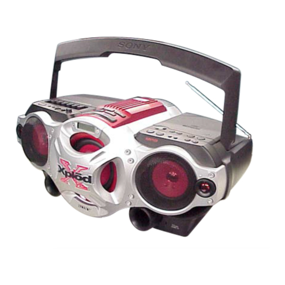
Photo : CFD-G555CP
Model Name Using Similar Mechanism
CD
CD Mechanism Type
Section
Optical Pick-up Type
Model Name Using Similar Mechanism
TAPE
Section
Tape Transport Mechanism Type
Q Q
3
6 7
1 3
1 5
SPECIFICATIONS
CD RADIO CASSETTE-CORDER
co
.
9 4
2 8
Canadian Model
CFD-G555CPK
E Model
Australian Model
CFD-G555CP
Mexican Model
CFD-G555CPK
CFD-G550CP
KSM-213CDP/C2NP
KSS-213C
CFD-G500/G550
MF-G500
0 5
8
2 9
9 4
2 8
Tape playback
Sony R20P: approx. 1.5 h
Sony alkaline LR20: approx. 6 h
CD playback
Sony R20P: approx. 1 h
Sony alkaline LR20: approx. 4 h
Dimensions
Approx. 530 × 241 × 369 mm (w/h/d)
(incl. projecting parts)
Mass
Approx. 8.0 kg (incl. batteries)
Supplied accessories
AC power cord (1)
Remote control (1)
• Abbreviation
AUS : Australian model
E41
: AC 230V area in E model
E92
: AC 120V area in E model
MX
: Mexican model
SP
: Singapore model
Design and specifications are subject to change
without notice.
m
9 9
9 9
Table of Contents

Related Manuals for Sony CFD-G555CP


Summary of Contents for Sony CFD-G555CP
- Page 1 Sony R20P: approx. 6 h Recording system Sony alkaline LR20: approx. 18 h 4-track 2 channel stereo CD RADIO CASSETTE-CORDER Fast winding time Approx. 120 s (sec.) with Sony cassette C-60 u163 Sony Corporation 9-887-100-02 Personal Audio Division 2006D16-1 Published by Sony Techno Create Corporation ©...
-
Page 2: Table Of Contents
7-2. Cabinet (Front) Section ........... 50 3-13. TUNER Board (CFD-G555CPK) ........16 7-3. Cabinet (Rear) Section ............ 51 3-14. H/P Board, TUNER Board (CFD-G555CP) ....16 7-4. Cabinet (Upper) (1) Section (CFD-G555CPK) ....52 3-15. MAIN Board ..............17 7-5. Cabinet (Upper) (1) Section (CFD-G555CP) ....53 3-16. -
Page 3: Servicing Notes
CFD-G555CP/G555CPK Ver. 1.1 SECTION 1 3 7 63 1515 0 SERVICING NOTES SAFETY CHECK-OUT NOTES ON HANDLING THE OPTICAL PICK-UP After correcting the original service problem, perform the following BLOCK OR BASE UNIT safety check before releasing the set to the customer: Check the antenna terminals, metal trim, “metallized”... -
Page 4: General
CFD-G555CP/G555CPK SECTION 2 This section is extracted from instruction manual. 3 7 63 1515 0 GENERAL CFD-G555CP (1/2) L 13942296513 u163 http://www.xiaoyu163.com... - Page 5 CFD-G555CP/G555CPK 3 7 63 1515 0 CFD-G555CP (2/2) L 13942296513 u163 http://www.xiaoyu163.com...
- Page 6 CFD-G555CP/G555CPK 3 7 63 1515 0 CFD-G555CPK (1/2) L 13942296513 u163 http://www.xiaoyu163.com...
- Page 7 CFD-G555CP/G555CPK 3 7 63 1515 0 CFD-G555CPK (2/2) L 13942296513 u163 http://www.xiaoyu163.com...
-
Page 8: Disassembly
3-2. CABINET (UPPER) (1) SECTION (Page 9) 3-3. CABINET (UPPER) (2) SECTION (Page 9) 3-4. CABINET (FRONT) SECTION (Page 10) CFD-G555CPK model CFD-G555CP model 3-10. CD KEY BOARD 3-12. CD KEY BOARD (Page 14) (Page 15) 3-11. MIC BOARD, POWER KEY BOARD,... -
Page 9: Cabinet (Upper) (1) Section
CFD-G555CP/G555CPK 3 7 63 1515 0 Note: Follow the disassembly procedure in the numerical order given. 3-2. CABINET (UPPER) (1) SECTION 1 Open the handle in the 4 two screws direction of the arrow. (+ BV tapping (B3) ) -
Page 10: Cabinet (Front) Section
CFD-G555CP/G555CPK 3 7 63 1515 0 3-4. CABINET (FRONT) SECTION 4 four screws BV tapping (B3) 3 four screws BV tapping (B3) cabinet (front) section 2 four screws BV tapping (B3) battery lid L 13942296513 3-5. TUNER KEY BOARD, VOL KEY BOARD... -
Page 11: Lcd Panel Assy
CFD-G555CP/G555CPK 3 7 63 1515 0 3-6. LCD PANEL ASSY 5 LCD panel assy 4 five screws BV tapping (B3) woofer speaker L 13942296513 1 two screws BV tapping (B3) 2 two screws BV tapping (B3) u163 http://www.xiaoyu163.com... -
Page 12: Led Board
CFD-G555CP/G555CPK 3 7 63 1515 0 3-7. LED BOARD 2 two claws 1 two claws light guide LED plate 6 LED 2 board 7 LED 3 board claw L 13942296513 claw 8 LED 4 board claw claw 5 LED 1 board Route the harnesses as shown below. -
Page 13: Lcd Board
CFD-G555CP/G555CPK 3 7 63 1515 0 3-8. LCD BOARD 3 two screws 1 two screws BV tapping (B3) BV tapping (B3) 4 two LED holders (L) 6 woofer cover 2 two LED holders (R) 5 alignment ring 7 three screws... -
Page 14: Power Board, Trans Board
CFD-G555CP/G555CPK 3 7 63 1515 0 3-9. POWER BOARD, TRANS BOARD qa two screws BV tapping (B3) 0 two screws BV tapping (B3) Remove the harnesses. 7 two screws BV tapping (B3) 9 screw BV tapping (B3) 2 CNP902 (4P) -
Page 15: Mic Board, Power Key Board, H/P Board (Cfd-G555Cpk)
(power) 8 screw PWH tapping (B2.6) 0 H/P board L 13942296513 3 CNP394 (3P) 9 CNP391 (9P) 3-12. CD KEY BOARD (CFD-G555CP) 3 two screws 2 ten screws PWH tapping (B2.6) BV tapping (B2.6) 5 screw BV tapping (B2.6) -
Page 16: Tuner Board (Cfd-G555Cpk)
1 two screws BV tapping (B3) Remove the soldering. TUNER board flexible flat cable (11core) (CNP1) L 13942296513 3-14. H/P BOARD, TUNER BOARD (CFD-G555CP) Remove the soldering. 1 two screws 5 screw BV tapping (B3) PWH tapping (B2.6) 6 JACK HOLD board... -
Page 17: Main Board
CFD-G555CP/G555CPK 3 7 63 1515 0 3-15. MAIN BOARD 5 three screws flexible flat cable (11 core) BV tapping (B3) Remove the soldering. qs MAIN board Remove the soldering. connector (2P) flexible flat cable flexible flat cable (11 core) -
Page 18: Optical Pick-Up (Kss-213C)
CFD-G555CP/G555CPK 3 7 63 1515 0 3-17. OPTICAL PICK-UP (KSS-213C) 5 optical pick-up 1 gear (A) claw 2 claw 4 sled shaft L 13942296513 3-18. TAPE MECHANISM DECK 1 three screws BV tapping (B3) 3 tape mechanism deck Open the cassette lid. -
Page 19: Tc Board
CFD-G555CP/G555CPK 3 7 63 1515 0 3-19. TC BOARD 1 screw 4 TC board Remove soldering from the four points. yellow red white black TC board 2 hook L 13942296513 3-20. MAIN BELT, SUB BELT 1 two screws ( +BIND DT M2 × 6) -
Page 20: Mechanical Adjustments
CFD-G555CP/G555CPK SECTION 4 SECTION 5 MECHANICAL ADJUSTMENTS 3 7 63 1515 0 ELECTRICAL ADJUSTMENTS PRECAUTION TAPE SECTION 0 dB = 0.775 V 1. Clean the following parts with a denatured-alcohol-moistened swab : • Standard Output Level record/playback head pinch roller... - Page 21 CFD-G555CP/G555CPK 3 7 63 1515 0 0 dB = 1 µV AM IF ADJUSTMENT TUNER SECTION Adjust for a maximum reading on level meter. • AM Section Setting: 450 kHz RADIO BAND•AUTO PRESET button: AM AM FREQUENCY COVERAGE ADJUSTMENT...
- Page 22 CFD-G555CP/G555CPK 3 7 63 1515 0 Adjustment Location: L3,CT3 AM TRACKING ADJUSTMENT L1,CT1 – TUNER BOARD (Component Side) – FM TRACKNG ADJUSTMENT TP-ANT (JW2) AM IF ADJUSTMENT FM IF ADJUSTMENT FM FREQUENCY AM FREQUENCY COVERAGE COVERAGE ADJUSTMENT ADJUSTMENT – TUNER BOARD (Conductor Side) –...
-
Page 23: Diagrams
CFD-G555CP/G555CPK Ver. 1.1 SECTION 6 3 7 6 3 1 5 1 5 0 DIAGRAMS • Circuit Boards Location THIS NOTE IS COMMON FOR PRINTED WIRING BOARDS AND SCHEMATIC DIAGRAMS. (In addition to this, the necessary note is printed in each block.) For Schematic Diagrams. -
Page 24: Block Diagram - Cd/Mp3 Section
CFD-G555CP/G555CPK 6-1. BLOCK DIAGRAM – CD/MP3 SECTION – 3 7 6 3 1 5 1 5 0 OPTICAL PICK-UP BLOCK (KSS-213C) MAIN LCHO SECTION CD L CH INTERPOLATION SLICE ERROR (Page 25) MUTE DIGITAL FIN2 EFMIN LEVEL CORRECTION &... -
Page 25: Block Diagram - Main Section
CFD-G555CP/G555CPK 6-2. BLOCK DIAGRAM – MAIN SECTION – 3 7 6 3 1 5 1 5 0 OVER LOAD WOOFER AMP IC351 Q351 WOOFER SP393 CONTROL WOOFER R.RO Q321-323 R.IN MUTE IC321 R.LINE REC/PB Q354 CD_IN_R CD/MP3 ELECTRONIC VOLUME... -
Page 26: Printed Wiring Board - Cd Section
CFD-G555CP/G555CPK 6-3. PRINTED WIRING BOARD – CD SECTION – • :Uses unleaded solder. • See page 23 for Circuit Boards Location. 3 7 6 3 1 5 1 5 0 G555CP G555CPK (Page 32) (Page 33) 1 3 9 4 2 2 9 6 5 1 3... -
Page 27: Schematic Diagram - Cd Section
CFD-G555CP/G555CPK • See page 42 for Waveforms. • See page 42, 43 for IC Block Diagrams. • See page 45 for IC Pin Function Description. 6-4. SCHEMATIC DIAGRAM – CD SECTION – 3 7 6 3 1 5 1 5 0... -
Page 28: Printed Wiring Board - Tuner Section
CFD-G555CP/G555CPK 6-5. PRINTED WIRING BOARD – TUNER SECTION – • :Uses unleaded solder. • See page 23 for Circuit Boards Location. 3 7 6 3 1 5 1 5 0 G555CP:E92/ G555CPK SP,E41,AUS (CV) G555CP MAIN BOARD FFC11P (Page 32) -
Page 29: Schematic Diagram - Tuner Section
CFD-G555CP/G555CPK 6-6. SCHEMATIC DIAGRAM – TUNER SECTION – • See page 42 for Waveforms. • See page 43 for IC Block Diagrams. 3 7 6 3 1 5 1 5 0 IC B/D JC12 JC11 G555CP: E92/ G555CPK SP,E41,AUS... -
Page 30: Printed Wiring Board - Tc Section
CFD-G555CP/G555CPK 6-7. PRINTED WIRING BOARD – TC SECTION – • See page 23 for Circuit Boards Location. • :Uses unleaded solder. 3 7 6 3 1 5 1 5 0 T301 C307 C305 R307 C304 R308 R306 C306 IC301... -
Page 31: Schematic Diagram - Tc Section
CFD-G555CP/G555CPK 6-8. SCHEMATIC DIAGRAM – TC SECTION – • See page 42 for Waveforms. • See page 44 for IC Block Diagram. 3 7 6 3 1 5 1 5 0 IC301 R103 R112 R301 IC B/D C102 R102... -
Page 32: Printed Wiring Boards - Main Section (G555Cp)
CFD-G555CP/G555CPK 6-9. PRINTED WIRING BOARDS – MAIN SECTION (G555CP) – • See page 23 for Circuit Boards Location. • :Uses unleaded solder. 3 7 6 3 1 5 1 5 0 CD KEY TUNER KEY BOARD BOARD BOARD KH401... -
Page 33: Printed Wiring Boards - Main Section (G555Cpk)
CFD-G555CP/G555CPK 6-10. PRINTED WIRING BOARDS – MAIN SECTION (G555CPK) – • See page 23 for Circuit Boards Location. • :Uses unleaded solder. 3 7 6 3 1 5 1 5 0 CD KEY TUNER KEY BOARD BOARD BOARD MIC BOARD... -
Page 34: Schematic Diagram - Main Section (1/3)
CFD-G555CP/G555CPK 6-11. SCHEMATIC DIAGRAM – MAIN SECTION (1/3) – • See page 44 for IC Block Diagram. 3 7 6 3 1 5 1 5 0 R364 R365 IC351 BA5417 C360 CNP393 D351 MC2840 SP393 Q351 KTC3198GR-AT R225 R125 R124 2.2k... -
Page 35: Schematic Diagram - Main Section (2/3)
CFD-G555CP/G555CPK 6-12. SCHEMATIC DIAGRAM – MAIN SECTION (2/3) – • See page 42 for Waveform. • See page 47 for IC Pin Function Description. 3 7 6 3 1 5 1 5 0 KHP805 R884 R885 C126 C226 Q803... -
Page 36: Schematic Diagram - Main (3/3), Control Section
CFD-G555CP/G555CPK 6-13. SCHEMATIC DIAGRAM – MAIN (3/3), CONTROL SECTION – 3 7 6 3 1 5 1 5 0 LCD401 R427 2.2k IC891 RPM7140-V4 L401 R443 2.2k C403 D402 1 50V C441 R428 L-7104SRD-H R469 100k C440 C444 C439... -
Page 37: Printed Wiring Boards - Control Section (G555Cp)
CFD-G555CP/G555CPK 6-14. PRINTED WIRING BOARDS – CONTROL SECTION (G555CP) – • See page 23 for Circuit Boards Location. • :Uses unleaded solder. 3 7 6 3 1 5 1 5 0 CD KEY BOARD P0WER MODE WOOFER KH401 SLEEP... -
Page 38: Printed Wiring Boards - Control Section (G555Cpk)
CFD-G555CP/G555CPK 6-15. PRINTED WIRING BOARDS – CONTROL SECTION (G555CPK) – • See page 23 for Circuit Boards Location. • :Uses unleaded solder. 3 7 6 3 1 5 1 5 0 CD KEY BOARD WOOFER FOLDER PRESET 1-869-451- TUNER KEY BOARD... -
Page 39: Printed Wiring Board - Power Section (G555Cp)
CFD-G555CP/G555CPK 6-16. PRINTED WIRING BOARD – POWER SECTION (G555CP) – • See page 23 for Circuit Boards Location. • :Uses unleaded solder. 3 7 6 3 1 5 1 5 0 BATTERY 1 BOARD BATTERY 2 BOARD POWER BOARD... -
Page 40: Printed Wiring Board - Power Section (G555Cpk)
CFD-G555CP/G555CPK 6-17. PRINTED WIRING BOARD – POWER SECTION (G555CPK) – • See page 23 for Circuit Boards Location. • :Uses unleaded solder. 3 7 6 3 1 5 1 5 0 BATTERY 1 BOARD BATTERY 2 BOARD POWER BOARD... -
Page 41: Schematic Diagram - Power Section
CFD-G555CP/G555CPK 6-18. SCHEMATIC DIAGRAM – POWER SECTION – 3 7 6 3 1 5 1 5 0 (Page 34) KH903 BATTERY BATTERY C901 C909 0.022uF 2200 D901 JW904 1N5401M CNJ901 D902 1N5401M JW903 JW919 C902 0.022uF F902 JW905 JW918 C903 0.022uF... - Page 42 CFD-G555CP/G555CPK 3 7 6 3 1 5 1 5 0 • Waveforms • IC Block Diagrams – CD/MP3 Board – – TUNER Board – – MAIN Board – – CD/MP3 Board – IC2 w; (XOUT) IC801 ek (X2) IC701 4 (RF)
- Page 43 CFD-G555CP/G555CPK 3 7 63 1515 0 – CD/MP3 Board – – TUNER Board – IC702 BA5826FP-E2 IC1 TA2149BN GND1 FM RF FM RF-OUT SP– D.BUFF VCC1 FM RF-IN SL– AM RF-IN D.BUFF AM LOW CUT LEVEL D.BUFF SHIFT MIX OUT FM OSC D.BUFF...
- Page 44 CFD-G555CP/G555CPK 3 7 63 1515 0 – MAIN Board – IC321 BD3870FS-E2 Treble1 Treble2 Bass2 Bass1 Logic fc=8kHz fc=8kHz fo=80Hz fo=80Hz Vcc/2 Vcc/2 0dB- -87dB Vcc/2 Vcc/2 Vcc/2 L 13942296513 – TC Board – IC301 TA2068N LINE L.LIN L.PO...
- Page 45 CFD-G555CP/G555CPK 3 7 63 1515 0 • IC PIN FUNCTION DESCRIPTION CD/MP3 BOARD IC1001 LC78684E-US-E (MP3 DECODER, CD-ROM DECODER, ANTI-SHOCK CONTROLLER) Pin No. Pin Name Description LRSY (I) CD L/R clock input ADDATA (O) Audio data output ADBCK (O)
- Page 46 CFD-G555CP/G555CPK 3 7 63 1515 0 Pin No. Pin Name Description DRAM write OK input (at CD-DA, H: active)/DRAM data request flag input WOK (I) (not used) Data connecting point detection completion flag output (at CD-DA, H: active)/DRAM CNTOK (O)
- Page 47 CFD-G555CP/G555CPK 3 7 63 1515 0 MAIN BOARD IC801 uPD7894216AGF-561-3BA-A (SYSTEM CONTROLLER) Pin No. Pin Name Description TU-CE PLL IC chip enable output TU-DATA PLL IC data output TU-CLK PLL IC clock output TU-COUNT PLL IC IF count data result input...
- Page 48 CFD-G555CP/G555CPK 3 7 63 1515 0 Pin No. Pin Name Description INTB(MP3) Decoder IC interrupt signal input WRQ(CD) CD interrupt signal input AVDD — Power supply pin (+3.3V) AVREF0 — Power supply pin (+3.3V) KEY1 A/D key input 1...
-
Page 49: Exploded Views
CFD-G555CP/G555CPK Ver. 1.1 SECTION 7 3 7 63 1515 0 EXPLODED VIEWS NOTE: • -XX and -X mean standardized parts, so they • The mechanical parts with no reference The components identified by mark 0 or may have some difference from the original number in the exploded views are not supplied. -
Page 50: Cabinet (Front) Section
CFD-G555CP/G555CPK 3 7 63 1515 0 7-2. CABINET (FRONT) SECTION L 13942296513 not supplied (LCD board) Ref. No. Part No. Description Remark Ref. No. Part No. Description Remark 2-657-087-01 FRAME, X PLODE 3-254-145-11 SCREW (B3), (+) BV TAPPING 2-657-083-11 PANEL, LCD 3-252-827-01 SCREW (B2.6), (+) BV TAPPING... -
Page 51: Cabinet (Rear) Section
CFD-G555CP/G555CPK Ver. 1.1 3 7 63 1515 0 7-3. CABINET (REAR) SECTION T901 F902 not supplied (BATTERY 2 board) L 13942296513 not supplied (BATTERY 1 board) Ref. No. Part No. Description Remark Ref. No. Part No. Description Remark 3-264-908-01 CHASSIS (TRANS) -
Page 52: Cabinet (Upper) (1) Section (Cfd-G555Cpk)
CFD-G555CP/G555CPK Ver. 1.1 3 7 63 1515 0 7-4. CABINET (UPPER) (1) SECTION (CFD-G555CPK) ANT1 S801 cabinet (upper) (2) section L 13942296513 supplied (JACK HOLD board) Ref. No. Part No. Description Remark Ref. No. Part No. Description Remark 3-252-828-01 SCREW (B2.6), (+) PWH TAPPING... -
Page 53: Cabinet (Upper) (1) Section (Cfd-G555Cp)
CFD-G555CP/G555CPK Ver. 1.1 3 7 63 1515 0 7-5. CABINET (UPPER) (1) SECTION (CFD-G555CP) ANT1 cabinet (upper) S801 (2) section supplied (JACK HOLD board) L 13942296513 Ref. No. Part No. Description Remark Ref. No. Part No. Description Remark 3-252-828-01 SCREW (B2.6), (+) PWH TAPPING... -
Page 54: Cabinet (Upper) (2) Section
CFD-G555CP/G555CPK 3 7 63 1515 0 7-6. CABINET (UPPER) (2) SECTION not supplied IC351 supplied Q972 not supplied Q971 IC371 tape mechanism deck section CD mechanism section L 13942296513 Ref. No. Part No. Description Remark Ref. No. Part No. -
Page 55: Tape Mechanism Deck Section
CFD-G555CP/G555CPK 3 7 63 1515 0 7-7. TAPE MECHANISM DECK SECTION M971 supplied supplied L 13942296513 HRP301 Ref. No. Part No. Description Remark Ref. No. Part No. Description Remark 2-663-212-01 BELT (B1), SUB 3-245-709-21 SCREW 2-663-211-01 BELT (B1), MAIN... -
Page 56: Optical Pick-Up Section (Ksm-213Cdp/C2Np)
CFD-G555CP/G555CPK 3 7 63 1515 0 7-8. OPTICAL PICK-UP SECTION (KSM-213CDP/C2NP) not supplied L 13942296513 M701 M702 Ref. No. Part No. Description Remark Ref. No. Part No. Description Remark 0 501 8-848-483-05 OPTICAL PICK-UP (KSS-213C/Q-RP) 2-626-907-11 GEAR (A) 2-174-500-01 SCREW (2X3) -
Page 57: Electrical Parts List
CFD-G555CP/G555CPK Ver. 1.1 SECTION 8 BATTERY 1 BATTERY 2 3 7 63 1515 0 ELECTRICAL PARTS LIST CD KEY CD/MP3 NOTE: • Due to standardization, replacements in the • RESISTORS When indicating parts by reference number, parts list may be different from the parts All resistors are in ohms. - Page 58 CFD-G555CP/G555CPK CD/MP3 3 7 63 1515 0 Ref. No. Part No. Description Remark Ref. No. Part No. Description Remark C753 1-162-923-11 CERAMIC CHIP 47PF < TRANSISTOR > C754 1-162-923-11 CERAMIC CHIP 47PF C756 1-162-923-11 CERAMIC CHIP 47PF Q701 8-729-054-57 TRANSISTOR...
- Page 59 CFD-G555CP/G555CPK CD/MP3 LED 1 3 7 63 1515 0 Ref. No. Part No. Description Remark Ref. No. Part No. Description Remark R766 1-216-797-11 METAL CHIP 1/10W C437 1-162-923-11 CERAMIC CHIP 47PF R1001 1-216-809-11 METAL CHIP 1/10W C438 1-162-923-11 CERAMIC CHIP...
- Page 60 CFD-G555CP/G555CPK LED 2 LED 3 LED 4 MAIN 3 7 63 1515 0 Ref. No. Part No. Description Remark Ref. No. Part No. Description Remark A-1167-870-A LED 2 BOARD, COMPLETE (G555CPK) C151 1-126-964-11 ELECT 10uF A-1167-978-A LED 2 BOARD, COMPLETE (G555CP)
- Page 61 CFD-G555CP/G555CPK MAIN 3 7 63 1515 0 Ref. No. Part No. Description Remark Ref. No. Part No. Description Remark C346 1-126-942-61 ELECT 1000uF C821 1-162-915-11 CERAMIC CHIP 10PF 0.5PF C348 1-128-548-11 ELECT 4700uF C823 1-104-658-91 ELECT 100uF C349 1-104-666-11 ELECT...
- Page 62 CFD-G555CP/G555CPK MAIN 3 7 63 1515 0 Ref. No. Part No. Description Remark Ref. No. Part No. Description Remark CNP806 1-815-443-11 PIN, CONNECTOR (PWB) 2P Q323 8-729-027-46 TRANSISTOR DTC114YKA-T146 < DIODE > Q351 8-729-036-89 TRANSISTOR KTC3198GR-AT Q352 8-729-028-90 TRANSISTOR...
- Page 63 CFD-G555CP/G555CPK MAIN 3 7 63 1515 0 Ref. No. Part No. Description Remark Ref. No. Part No. Description Remark R253 1-216-829-11 METAL CHIP 4.7K 1/10W R433 1-216-841-11 METAL CHIP 1/10W (G555CPK) (G555CPK) R434 1-216-821-11 METAL CHIP 1/10W R254 1-216-833-11 METAL CHIP...
- Page 64 CFD-G555CP/G555CPK MAIN 3 7 63 1515 0 Ref. No. Part No. Description Remark Ref. No. Part No. Description Remark R833 1-216-841-11 METAL CHIP 1/10W R889 1-216-841-11 METAL CHIP 1/10W R834 1-216-821-11 METAL CHIP 1/10W R890 1-216-841-11 METAL CHIP 1/10W...
- Page 65 CFD-G555CP/G555CPK Ver. 1.1 POWER POWER KEY TRANS 3 7 63 1515 0 Ref. No. Part No. Description Remark Ref. No. Part No. Description Remark < RESISTOR > A-1167-863-A TRANS BOARD, COMPLETE (including POWER BOARD, COMPLETE) (MX) R426 1-216-821-11 METAL CHIP...
- Page 66 CFD-G555CP/G555CPK Ver. 1.1 TUNER 3 7 63 1515 0 Ref. No. Part No. Description Remark Ref. No. Part No. Description Remark R103 1-216-843-11 METAL CHIP 1/10W 1-162-970-11 CERAMIC CHIP 0.01uF R104 1-216-835-11 METAL CHIP 1/10W (SP, E41, AUS) R105...
- Page 67 CFD-G555CP/G555CPK TUNER TUNER KEY VOL KEY 3 7 63 1515 0 Ref. No. Part No. Description Remark Ref. No. Part No. Description Remark < DIODE > 1-216-809-11 METAL CHIP 1/10W 1-216-825-11 METAL CHIP 2.2K 1/10W 8-719-078-48 DIODE KV1471ETR-G 8-719-078-48 DIODE KV1471ETR-G 1-216-825-11 METAL CHIP 2.2K...
- Page 68 CFD-G555CP/G555CPK Ver. 1.1 3 7 63 1515 0 Ref. No. Part No. Description Remark MISCELLANEOUS ************** 1-831-781-21 CABLE, FLEXIBLE FLAT (11 CORE) 1-452-732-11 MAGNET 1-452-732-11 MAGNET 1-832-026-11 CABLE, FLEXIBLE FLAT (16 CORE) 1-831-730-21 CABLE, FLEXIBLE FLAT (20 CORE) 1-831-778-21 CABLE, FLEXIBLE FLAT (11 CORE)
- Page 69 CFD-G555CP/G555CPK 3 7 63 1515 0 MEMO L 13942296513 u163 http://www.xiaoyu163.com...
- Page 70 CFD-G555CP/G555CPK 3 7 63 1515 0 REVISION HISTORY Clicking the version allows you to jump to the revised page. Also, clicking the version at the upper right on the revised page allows you to jump to the next revised page.