Sony CDP-XB720 Service Manual
Hide thumbs
Also See for CDP-XB720:
- Operating instructions manual (64 pages) ,
- Service manual (41 pages) ,
- Operating instructions manual (64 pages)
Table of Contents
Quick Links
Table of Contents

Related Manuals for Sony CDP-XB720


Summary of Contents for Sony CDP-XB720
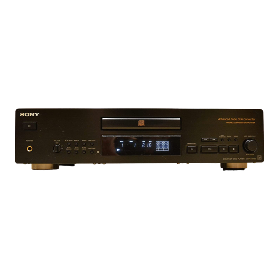
- Page 1 CDP-XB720/XB720E SERVICE MANUAL AEP Model CDP-XB720 UK Model CDP-XB720E Photo: CDP-XB720 Model Name Using Similar Mechanism CDP-XE520 CD Mechanism Type CDM14FLS-5BD25 Base Unit Type BU-5BD25 Optical Pick-up Type KSS-213BA/F-NP SPECIFICATIONS COMPACT DISC PLAYER MICROFILM – 1 –...
-
Page 2: Table Of Contents
WITH MARK ! ON THE SCHEMATIC DIAGRAMS AND IN THE PARTS LIST ARE CRITICAL TO SAFE OPERATION. REPLACE THESE COMPONENTS WITH SONY PARTS WHOSE PART NUMBERS APPEAR AS SHOWN IN THIS MANUAL OR IN SUPPLEMENTS PUBLISHED BY SONY. – 2 –... -
Page 3: Servicing Note
SECTION 1 SERVICING NOTE HOW TO OPEN THE DISC TRAY WHEN POWER SWITCH NOTES ON HANDLING THE OPTICAL PICK-UP BLOCK TURNS OFF OR BASE UNIT Insert a tapering driver into the aperture of the unit bottom, and turn The laser diode in the optical pick-up block may suffer in the direction of arrow. - Page 4 CD-TEXT TEST DISC This unit is able to display the TEXT data (character information) written in the CD on its fluorescent indicator tube. The CD-TEXT TEST DISC (TGCS-313: J-2501-126-A) is used for checking the display. To check, perform the following procedure. Procedure: 1.
- Page 5 Table 2: CD-TEXT TEST DISC Recorded Contents and Display (In this unit, some special characters cannot be displayed. This is no a fault.) TRACK Recorded contents Display ! ” # $ % & ´ (21h to 27h)1kHz 0dB L&R ···· ! ” # $ % & are not displayed + , –...
-
Page 6: General
SECTION 2 GENERAL Front Panel LOCATION OF PARTS AND CONTROLS 1 1/u (power) switch 2 PLAY MODE button 3 REPEAT button 4 FADER button 5 TIME/TEXT button 6 Disc tray 7 0,) button 8 EDIT/TIME FADE button 9 CHECK button 10 CLEAR button 11 AMS knob (PUSH ENTER) 12 p (stop) button... -
Page 7: Disassembly
SECTION 3 DISASSEMBLY Note : Follow the disassembly procedure in the numerical order given. 3-1. FRONT PANEL • In order to remove the front panel block when the power supply does not turn on, rotate the cam with tapering driver as the figure shows, and the loading part will be moved. -
Page 8: Test Mode
SECTION 4 TEST MODE 4-1. AF MODE Button No. Button No. Button Button The following checks can be performed in the AF mode, which is Displayed Displayed set by connecting the JW004 (AFADJ) terminal on MAIN LANGUAGE EDIT/ board to the Ground and turning on the power. MUSIC SCAN TIME FADE •... - Page 9 4-3. AGING MODE [ MAIN BOARD ] – Component Side – This unit is equipped with an aging mode to check operations of the mechanism deck. • When faults occur: Aging stops, and the state when aging stopped is displayed on the fluorescent display tube.
-
Page 10: Electrical Block Checking
SECTION 5 ELECTRICAL BLOCK CHECKING S-curve waveform Note: 1. CD Block is basically designed to operate without adjustment. symmetry Therefore, check each item in order given. 2. Use YEDS-18 disc (3-702-101-01) unless otherwise indicated. 3. Use an oscilloscope with more than 10MΩ impedance. 4. - Page 11 1 track jump waveform Adjustment Location : Center of the waveform [ MAIN BOARD ] – Component Side – A (DC voltage) + 0.7 level : 1.3 Vp-p symmetry – 0.6 JW004 (AFADJ) E-F Balance Check (With general remote commander) JW003 oscilloscope (ADJ)
-
Page 12: Diagrams
SECTION 6 DIAGRAMS 6-1. CIRCUIT BOARDS LOCATION POWER board BD board SW board HP board (AEP) DF board MAIN board LOADING board PANEL board – 12 –... - Page 13 THIS NOTE IS COMMON FOR PRINTED WIRING BOARDS AND SCHEMATIC DIAGRAMS. (In addition to this, the necessary note is printed in each block.) For schematic diagrams. Note: • All capacitors are in µF unless otherwise noted. pF: µµF 50 WV or less are not indicated except for electrolytics and tantalums.
- Page 14 WAVEFORMS 3.9Vp-p 5.5 Vp-p 33.8MHz 2.82 MHz IC101 &¡ XTAI IC301 $º 64FSO 1.2Vp-p 1.3 Vp-p (PLAY) 45 MHz IC101 %º RF AC IC301 @• XOUT 2.5V 5.3 Vp-p APPROX 500mVp-p (PLAY) 2.1 MHz IC101 $¡ TE IC301 2 BCK I !º...
-
Page 15: Printed Wiring Board - Bd Section
CDP-XB720/XB720E 6-2. PRINTED WIRING BOARD – BD SECTION – • See page 12 for Circuit Boards Location. • Semiconductor Location Ref. No. Location IC102 Q101 – 15 –... - Page 16 (Page 19) • Semiconductor Location Ref. No. Location IC101 IC103 – 16 –...
-
Page 17: Schematic Diagram - Bd Section
CDP-XB720/XB720E 6-3. SCHEMATIC DIAGRAM – BD SECTION – • See page 14 for Waveforms. • See page 30 for IC Pin Functions. • See page 34 for IC Block Diagrams. (Page 21) – 18 – – 17 –... -
Page 18: Printed Wiring Board - Main Section
CDP-XB720/XB720E 6-4. PRINTED WIRING BOARD – MAIN SECTION – • See page 12 for Circuit Boards Location. (Page 28) • Semiconductor Location Ref. No. Location D631 D651 D679 D680 D681 D682 D691 D692 D721 IC301 IC401 IC451 IC631 IC651 IC652... -
Page 19: Schematic Diagram - Main Section
CDP-XB720/XB720E 6-5. SCHEMATIC DIAGRAM – MAIN SECTION – • See page 36 for IC Block Diagrams. (Page 17) (Page 29) (Page 27) (Page (Page 27) – 21 – –22 –... - Page 20 CDP-XB720/XB720E 6-6. PRINTED WIXRING BOARD – DISPLAY SECTION – • See page 12 for Circuit Boards Location. (Page 21) • Semiconductor Location Ref. No. Location IC501 IC502 Q501 Q502 – 24 – – 23 –...
-
Page 21: Schematic Diagram - Display Section
CDP-XB720/XB720E 6-7. SCHEMATIC DIAGRAM – DISPLAY SECTION – • See page 32 for IC Pin Functions. (Page 21) – 25 – – 26 –... -
Page 22: Schematic Diagram - Power/Hp Section
CDP-XB720/XB720E 6-8. SCHEMATIC DIAGRAM – POWER/HP SECTION – (Page 22) (Page – 27 –... -
Page 23: Printed Wiring Board - Power/Hp Section
6-9. PRINTED WIRING BOARD – POWER/HP SECTION – • See page 12 for Circuit Boards Location. (Page 20) (Page – 28 –... -
Page 24: Schematic Diagram - Loading Motor Section
CDP-XB720/XB720E 6-10. SCHEMATIC DIAGRAM – LOADING MOTOR SECTION – (Page 21) 6-11. PRINTED WIRING BOARD – LOADING MOTOR SECTION – • See page 12 for Circuit Boards Location. LOADING BOARD S152 LOAD CN151 S151 LOAD M151 LOADING (Page 19) MOTOR... -
Page 25: Ic Pin Functions
6-12. IC PIN FUNCTIONS • IC101 DIGITAL SIGNAL PROCESSOR (CXD2585Q) Pin No. Pin Name Function – DVDD Digital power supply XRST System reset “L” : reset MUTE Muting input “H” : mute DATA Serial data input, supplied from CPU XLAT Latch input, supplied from CPU CLOK Serial data transfer clock input, supplied from CPU... - Page 26 Pin No. Pin Name Function Tracking error signal input Center servo analog input RFDC RF signal input Test pin (Not used) ADIO – Analog ground AVSS0 Stabilized current input for operational amplifiers IGEN – Analog power supply AVDD0 EFM full swing output ASYO Asymmetry comparate voltage input ASYI...
- Page 27 • IC501 SYSTEM CONTROL (CXP82832-009Q) Pin Name Function Pin No. FL grid signal output FL grid signal output – Connected to VDD – Power supply (+5V) SCOR Sub code sync input 6, 7 – Ground RMIN Remote control signal input –...
- Page 28 Pin Name Function Pin No. – Ground – Not used – Connected to ground VDD (+5V) – Power supply (+5V) VFDP (–30V) – Pull down voltage (–30V) XSEL Not used REINIT – Not used LP CONTROL LP control hold output B-MUTE Line mute control output 50 to 66...
-
Page 29: Ic Block Diagrams
6-13. IC BLOCK DIAGRAMS • BD section IC101 CXD2585Q 71 70 64 63 62 61 67 66 65 Digital VPCO Clock DVDD0 V16M Generator XRST VCTL MUTE Interface BIAS Error AVDD1 Corrector DATA XLAT CLOCK FILI Interface Digital Sub Code FILO demodurator Processor... - Page 30 IC102 BA6392FP BUFF CH1 OUT F 28 GND BUFF BUFF CH1 OUT R 27 CH4 OUT F LEVEL SHIFT CAPA IN 1 26 CH4 OUT R BUFF CH1 R IN 25 VB IN INTERFACE CH1 F IN 24 VS IN BUFF VREF IN 23 VB IN...
-
Page 31: Main Section
• Main section IC301 CXD8735N INVO INVI BCKI TEST OVERFLOW DETECTER DATA1 128FsO FIR1 FIR2 FIR3 LRCKI DINIT FIR4 INIT OVFLAG MUTEL OVERFLOW DETECTER SHIFT MUTER FIR1 FIR2 FIR3 LATCH FIR4 SYSM 64FSI MCKIN 3rd order X0.75 L.I.P NOISE DVSS1 SHAPER DITHER DVSS1... -
Page 32: Exploded Views
SECTION 7 EXPLODED VIEWS NOTE: The components identified by • Items marked “*” are not stocked since they are mark ! or dotted line with mark seldom required for routine service. Some delay ! are critical for safety. should be anticipated when ordering these items. Replace only with part number •... -
Page 33: Front Panel Section
Part No. Description Remark Ref. No. Part No. Description Remark 4-942-568-41 EMBLEM (NO.5), SONY 4-997-213-01 BUTTON (F.R) 4-998-790-01 KNOB, POWER 4-974-510-01 SCREW (+BV 3X8 B)(UK) * 53 1-668-724-11 SW BOARD 7-685-646-79 SCREW +BVTP 3X8 TYPE2 N-S (AEP) 4-951-620-01 SCREW (2.6X8), +BVTP... -
Page 34: Mechanism Deck Section (Cdm14Fls-5Bd25)
7-3. MECHANISM DECK SECTION (CDM14FLS-5BD25) BU-5BD25 not supplied M151 Ref. No. Part No. Description Remark Ref. No. Part No. Description Remark 1-452-925-21 MAGNET ASSY 4-933-134-01 SCREW +PTPWH M2.6X6 4-933-110-41 HOLDER (MG) 4-995-814-11 TABLE (FL), DISC 4-959-996-01 SPRING (932), COMPRESSION 4-967-268-01 GEAR (C) 4-933-129-01 HOLDER (BU) 4-927-649-01 BELT 4-933-111-11 CHASSIS (MD) -
Page 35: Base Unit Section (Bu-5Bd25)
7-4. BASE UNIT SECTION (BU-5BD25) M102 M101 The components identified by mark ! or dotted line with mark ! are critical for safety. Replace only with part number specified. Ref. No. Part No. Description Remark Ref. No. Part No. Description Remark ! 151 8-848-379-31 OPTICAL PICK-UP KSS-213BA/F-NP... -
Page 36: Electrical Parts List
SECTION 8 ELECTRICAL PARTS LIST Note: • SEMICONDUCTORS • Due to standardization, replacements in the parts list The components identified by In each case, u: µ , for example: may be different from the parts specified in the mark ! or dotted line with mark uA...: µ... - Page 37 LOADING MAIN Ref. No. Part No. Description Remark Ref. No. Part No. Description Remark < SWITCH > < CAPACITOR > S101 1-572-085-11 SWITCH, LEAF (LIMIT) C301 1-161-494-00 CERAMIC 0.022uF C351 1-102-945-00 CERAMIC 8.0PF ±0.5PF 50V C352 1-102-945-00 CERAMIC 8.0PF ±0.5PF 50V ************************************************************** C353 1-136-850-11 FILM...
- Page 38 MAIN Ref. No. Part No. Description Remark Ref. No. Part No. Description Remark C670 1-162-294-31 CERAMIC 0.001uF J721 1-774-726-11 JACK (S-LINK CONTROL A1) J781 1-778-228-11 JACK, PIN 1P (DIGITAL OUT:COAXIAL)(AEP) C671 1-126-962-11 ELECT 3.3uF J781 1-784-689-11 JACK, PIN 1P (DIGITAL OUT:COAXIAL)(UK) C672 1-164-159-21 CERAMIC 0.1uF...
- Page 39 MAIN PANEL Ref. No. Part No. Description Remark Ref. No. Part No. Description Remark R462 1-249-411-11 CARBON 1/4W IC502 8-749-014-66 IC NJL64H400A R463 1-249-411-11 CARBON 1/4W R464 1-249-441-11 CARBON 100K 1/4W < TRANSISTOR > R465 1-247-807-31 CARBON 1/4W Q501 8-729-029-66 TRANSISTOR DTC114ESA Q502 8-729-029-66 TRANSISTOR DTC114ESA R631...
- Page 40 PANEL POWER Ref. No. Part No. Description Remark Ref. No. Part No. Description Remark S522 1-554-303-21 SWITCH, TACTILE (·) R641 1-247-843-11 CARBON 3.3K 1/4W R642 1-247-843-11 CARBON 3.3K 1/4W S523 1-554-303-21 SWITCH, TACTILE (P) R643 1-212-873-11 FUSIBLE 1/4W F S524 1-554-303-21 SWITCH, TACTILE (p) R644 1-247-807-31 CARBON...
- Page 41 CDP-XB720/XB720E Ref. No. Part No. Description Remark ************** HARDWARE LIST ************** 7-685-871-01 SCREW +BVTT 3X6 (S) 7-685-885-09 SCREW +BVTT 4X16 (S) 7-621-775-10 SCREW +B 2.6X4 7-621-255-15 SCREW +P 2X3 7-685-134-19 SCREW +BTP 2.6X8 TYPE2 N-S 98F097549-1 Sony Corporation Printed in Hungary © 1998. 6 9-922-853-11 Home A&V Products Company...