Table of Contents
CDX-GT06/CXS-GT06HP
SERVICE MANUAL
Ver. 1.0 2006.07
• CXS-GT06HP is composed of CDX-GT06,
2 way speaker, 3 way speaker.
• The tuner and CD sections have no adjustments.
AUDIO POWER SPECIFICATIONS
POWER OUTPUT AND TOTAL HARMONIC DISTORTION
22 watts per channel minimum continuous average power into
4 ohms, 4 channels driven from 20 Hz to 20 kHz with no more
than 5% total harmonic distortion.
CD Player section
Signal-to-noise ratio:
120 dB
Frequency response:
10 – 20,000 Hz
Wow and flutter:
Below measurable limit
Tuner section
FM
Tuning range:
87.5 – 107.9 MHz
Antenna terminal:
External antenna connector
Intermediate frequency: 10.7 MHz/450 kHz
Usable sensitivity:
9 dBf
Selectivity:
75 dB at 400 kHz
Signal-to-noise ratio:
67 dB (stereo), 69 dB (mono)
Harmonic distortion at 1 kHz:
0.5 % (stereo), 0.3 % (mono)
Separation:
35 dB at 1 kHz
Frequency response:
30 – 15,000 Hz
AM
Tuning range:
530 – 1,710 kHz
Antenna terminal:
External antenna connector
Intermediate frequency: 10.7 MHz/450 kHz
Sensitivity:
30 µV
Sony Corporation
9-887-357-01
eVehicle Division
2006G04-1
Published by Sony Techno Create Corporation
© 2006.07
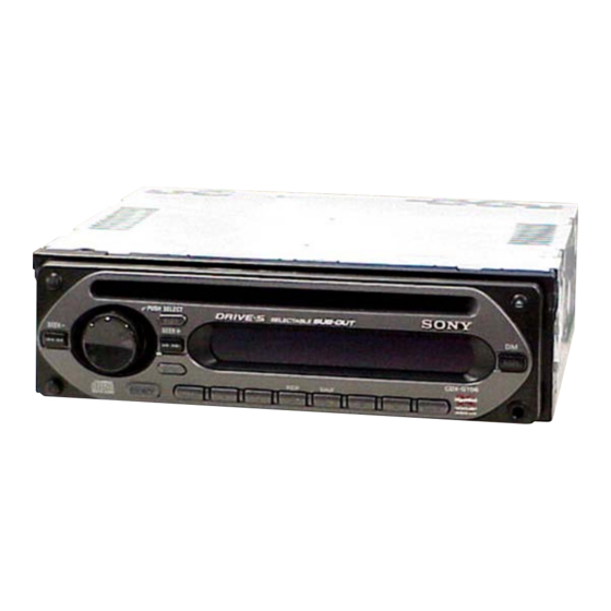
(Photo: CDX-GT06)
Model Name Using Similar Mechanism
CD Drive Mechanism Type
Optical Pick-up Name
SPECIFICATIONS
Power amplifier section
Outputs:
Speaker impedance:
Maximum power output: 45 W × 4 (at 4 ohms)
General
Outputs:
Inputs:
Tone controls:
Power requirements:
Dimensions:
Mounting dimensions:
Mass:
Supplied accessories:
FM/AM COMPACT DISC PLAYER
US Model
CDX-GT10W/GT100
MG-611XE-186//C
KSS1000E
Speaker outputs (sure seal connectors)
4 – 8 ohms
Audio outputs terminal (sub/rear switchable)
Power antenna relay control terminal
Power amplifier control terminal
Antenna input terminal
AUX input jack (stereo mini jack)
Low: ±10 dB at 60 Hz (XPLOD)
Mid: ±10 dB at 1 kHz (XPLOD)
High: ±10 dB at 10 kHz (XPLOD)
12 V DC car battery (negative ground)
Approx. 178 × 50 × 179 mm
(7
× 2 × 7
in) (w/h/d)
1/8
1/8
Approx. 182 × 53 × 161 mm
(7
× 2
× 6
in) (w/h/d)
1/4
1/8
3/8
Approx. 1.2 kg (2 lb 11 oz)
Parts for installation and connections (1 set)
– Continued on next page –
Table of Contents

Related Manuals for Sony CDX-GT06


Summary of Contents for Sony CDX-GT06
- Page 1 CDX-GT06/CXS-GT06HP SERVICE MANUAL US Model Ver. 1.0 2006.07 • CXS-GT06HP is composed of CDX-GT06, (Photo: CDX-GT06) 2 way speaker, 3 way speaker. • The tuner and CD sections have no adjustments. Model Name Using Similar Mechanism CDX-GT10W/GT100 CD Drive Mechanism Type...
- Page 2 COMPONENTS IDENTIFIED BY MARK 0 OR DOTTED LINE WITH MARK 0 ON THE SCHEMATIC DIAGRAMS AND IN THE PARTS LIST ARE CRITICAL TO SAFE OPERATION. REPLACE THESE COMPONENTS WITH SONY PARTS WHOSE PART NUMBERS APPEAR AS SHOWN IN THIS MANUAL OR IN SUPPLEMENTS PUBLISHED BY SONY.
- Page 3 CDX-GT06/CXS-GT06HP SERVICE NOTES Notes on Chip Component Replacement • Never reuse a disconnected chip component. CAUTION • Notice that the minus side of a tantalum capacitor may be damaged Use of controls or adjustments or performance of procedures other by heat.
-
Page 4: Table Of Contents
CDX-GT06/CXS-GT06HP TEST DISCS TABLE OF CONTENTS Please use the following test discs for the check on the voltage and the waveforms of the CD section. GENERAL Location of Controls and Basic Operations ....5 YDES-18 (Part No. 3-702-101-01) Connections ..............5 PATD-012 (Part No. -
Page 5: General
CDX-GT06/CXS-GT06HP SECTION 1 GENERAL This section is extracted from instruction manual. Location of controls and basic operations Main unit CDX-GT06 1 OFF button 0 SOURCE button To power off; stop the source. To power on; change the source (Radio/CD/ AUX). -
Page 6: Connection Diagram
CDX-GT06/CXS-GT06HP Power amplifi er (not supplied) Amplifi cador de potencia (no suministrado) Active subwoofer (not supplied) Altavoz potenciador de graves activo (no suministrado) Rear speaker (not supplied) Altavoz posterior RCA pin cord (not supplied) (no suministrado) AUDIO OUT can be switched to SUB or REAR. -
Page 7: Disassembly
CDX-GT06/CXS-GT06HP SECTION 2 DISASSEMBLY Note: This set can be disassemble according to the following sequence. 2-1. SUB PANEL ASSY (Page 8) 2-2. CD MECHANISM BLOCK (Page 8) 2-10. SERVO BOARD 2-3. MAIN BOARD 2-4. CHASSIS (T) SUB ASSY (Page 12) -
Page 8: Sub Panel Assy
CDX-GT06/CXS-GT06HP Note: Follow the disassembly procedure in the numerical order given. 2-1. SUB PANEL ASSY 3 two claws 2 two claws 1 two screws (+PTT 2.6 × 6) 4 sub panel assy 2-2. CD MECHANISM BLOCK 6 bracket (CD) 7 CD mechanism block 5 two screws (+PTT 2.6 ×... -
Page 9: Main Board
CDX-GT06/CXS-GT06HP 2-3. MAIN BOARD 1 three screws (+BTT 2.6 × 5) 2 two screws (+PTT 2.6 × 8) 3 MAIN board 2-4. CHASSIS (T) SUB ASSY 4 claw 2 two screws (+P 1.7 × 2.2) 1 two screws (+P 1.7 × 2.2) -
Page 10: Roller Arm Assy
CDX-GT06/CXS-GT06HP 2-5. ROLLER ARM ASSY 3 washer (1.1-2.5) 5 roller arm assy 4 gear (RA1) 2 spring (RAR) 1 spring (RAL) 2-6. CHASSIS (OP) ASSY 0 chassis (OP) assy 9 compression spring (damper) lever (D) 1 optical pick-up (16 core) -
Page 11: Optical Pick-Up
CDX-GT06/CXS-GT06HP 2-7. OPTICAL PICK-UP 2 chucking arm sub assy 5 claw 1 tension spring (CHKG) 7 optical pick-up 6 main shaft 4 rack (SL) 3 screw (+B 1.4 × 5) 2-8. SL MOTOR ASSY (M902) 1 screw (+P 1.4 × 1.8) -
Page 12: Le Motor Assy (M903)
CDX-GT06/CXS-GT06HP 2-9. LE MOTOR ASSY (M903) 7 screw 9 gear (LE) assy (+M 1.7 × 2.5) 8 bearing (LEB-N) 0 screw (+M 1.7 × 2.5) qd two toothed lock screws 2 gear (LE1) (+M 1.4 ) lever (D) bracket (LEM-N) -
Page 13: Diagrams
CDX-GT06/CXS-GT06HP SECTION 3 DIAGRAMS 3-1. BLOCK DIAGRAM — CD SECTION — • R-ch is omitted due to same as L-ch. • Siganal Path : CD PLAY DETECTOR MAIN 77 AGCI AGCO 71 RFI 69 ASY LOUT CD-L SECTION (Page 14) -
Page 14: Block Diagram -Main Section
CDX-GT06/CXS-GT06HP 3-2. BLOCK DIAGRAM — MAIN SECTION — ELECTRONIC VOLUME IC401 (Page 13) CD-L 9 CD LCH J330 SECTION OUT SUB-L AUDIO OUT R-CH 8 CD RCH OUT SUB-R R-CH REAR R-CH R-CH J901 5 AUX LCH I2C-BUS 3 AUX RCH... -
Page 15: Block Diagram -Display Section
CDX-GT06/CXS-GT06HP 3-3. BLOCK DIAGRAM — DISPLAY SECTION — • NOTE FOR PRINTED WIRING BOARDS AND SCHEMATIC DIAGRAMS THIS NOTE IS COMMON FOR PRINTED WIRING SYSTEM CONTROL LCD DRIVER BOARDS AND SCHEMATIC DIAGRAMS. IC501 (3/3) IC901 (In addition to this, the necessary note is printed in each block.) -
Page 16: Printed Wiring Boards -Cd Mechanism Section
CDX-GT06/CXS-GT06HP 3-5. PRINTED WIRING BOARDS — CD MECHANISM SECTION — • Refer to page 15 for Circuit Boards Location. : Uses unleaded solder. (Page 18) CDX-GT06/CXS-GT06HP... -
Page 17: Schematic Diagram -Cd Mechanism Section
CDX-GT06/CXS-GT06HP • Refer to page 24 for Waveforms. • Refer to page 24 for IC Block Diagram. 3-6. SCHEMATIC DIAGRAM — CD MECHANISM SECTION — • Refer to page 27 for IC Pin Description of IC1. TP19 TP32 TP33 R14 R15... -
Page 18: Printed Wiring Board -Main Section
CDX-GT06/CXS-GT06HP 3-7. PRINTED WIRING BOARD — MAIN SECTION — • Refer to page 15 for Circuit Boards Location. : Uses unleaded solder. J330 • Semiconductor Location Ref. No. Location D479 D503 D580 F-11 D581 F-11 D601 C-10 D609 D617 D719... -
Page 19: Schematic Diagram -Main Section (1/3)
CDX-GT06/CXS-GT06HP 3-8. SCHEMATIC DIAGRAM — MAIN SECTION (1/3) — • Refer to page 25 for IC Block Diagram. C484 J330 IC B/D IC401 C474 C401 FB411 FB410 C411 C410 C413 C405 C404 C435 C432 R431 R405 C431 C412 Q431 R432... -
Page 20: Schematic Diagram -Main Section (2/3)
CDX-GT06/CXS-GT06HP 3-9. SCHEMATIC DIAGRAM — MAIN SECTION (2/3) — • Refer to page 26 for IC Block Diagram. JC795 C774 C775 C765 C764 IC B/D C751 D751 D752 C750 D753 D754 JC754 JC755 D755 D756 IC750 TDA8589BJ/N2/R1 D757 CN601 D758... -
Page 21: Schematic Diagram -Main Section (3/3)
CDX-GT06/CXS-GT06HP • Refer to page 24 for Waveforms. 3-10. SCHEMATIC DIAGRAM — MAIN SECTION (3/3) — • Refer to page 29 for IC Pin Description of IC501. (Page 19) (Page 20) (Page 17) L301 FB603 D719 CN701 FB304 CNP301 R516... -
Page 22: Printed Wiring Boards -Key Section
CDX-GT06/CXS-GT06HP 3-11. PRINTED WIRING BOARDS — KEY SECTION — • Refer to page 15 for Circuit Boards Location. : Uses unleaded solder. (Page 18) MAIN BOARD CN701 • Semiconductor Location Ref. No. Location D901 H-10 D903 H-10 D981 H-10 D982... -
Page 23: Schematic Diagram -Key Section
CDX-GT06/CXS-GT06HP 3-12. SCHEMATIC DIAGRAM — KEY SECTION — R981 LSW909(2/2) LSW908(2/2) R982 LSW902(2/2) LSW919(2/2) LSW916(2/2) LSW914(2/2) R943 R952 R955 R957 R931 R941 R956 R958 LSW918(2/2) LSW913(2/2) LSW903(2/2) R932 LED951 LSW910(2/2) LSW911(2/2) R933 R942 LSW920(2/2) LSW917(2/2) LSW915(2/2) LSW912(2/2) LSW901(2/2) LED932 IC901... - Page 24 CDX-GT06/CXS-GT06HP • WAVEFORMS • IC BLOCK DIAGRAMS — SERVO Board — (CD PLAY) — MAIN Board — IC2 BA5966FP-FE2 (SERVO Board) IC1 wd (XTAL) IC501 i; (XIN) 0.7Vp-p 1.2Vp-p OPIN4+ LDCTL 32.768 kHz OUTR OUTF 16.9344MHz OPIN4– OPOUT1 OPOUT4 0.2 V/DIV, 0.2 µ sec/DIV 0.2 V/DIV, 0.1 µ...
- Page 25 CDX-GT06/CXS-GT06HP IC401 BD3806AFS-E2 (MAIN Board (1/3)) FADER FADER FADER FADER (0~-58, (0~-58, (0~-58, (0~-58, C BUS -∞dB) -∞dB) -∞dB) -∞dB) GAIN+ATT LOGIC (+10~-29, -∞dB) 2ND ORDER LPF fc:OFF,80,120,160Hz 2ND ORDER Q: 0.707 BASS fo:60,70,80,100,120,140,160,200Hz TONE TONE Q:0.5,0.75,1,1.25 PASS PASS MIDDLE...
- Page 26 CDX-GT06/CXS-GT06HP IC750 TDA8589BJ/N2/R1 (MAIN Board (2/3)) OUT-FL- C BUS OUT-FL+ OUT-RL- PGND3 OUT-RL+ IN-RL IN-FL S-GND PROTECTION/ DIAGNOSTIC IN-FR IN-RR BEEP OUT-RR+ PGND2 OUT-RR- OUT-FR+ STANDBY/ MUTE OUT-FR- CHIP DETECT/ PGND1 DIAGNOSTIC BATTERY TEMPERATURE DIAG DETECTION PROTECTION ENABLE LOGIC ANT-REM...
- Page 27 CDX-GT06/CXS-GT06HP • IC PIN DESCRIPTIONS IC1 µPD63712GC-8EU-A (RF AMP, DIGITAL SERVO, DIGITAL SIGNAL PROCESSOR) (SERVO BOARD) Pin No. Pin Name Pin Description Laser diode ON/OFF control signal output (L: laser OFF, H: laser ON) Dimmer monitor input from optical pick-up laser diode.
- Page 28 CDX-GT06/CXS-GT06HP Pin No. Pin Name Pin Description SCKIN Not used. (Connect to SCKO in this set.) SCKO Not used. (Connect to SCKIN in this set.) LRCKIN Not used. (Connect to LRCK in this set.) LRCK Not used. (Connect to LRCKIN in this set.) DVDD —...
- Page 29 CDX-GT06/CXS-GT06HP IC501 MB90488BPF-G-186-AE1 (SYSTEM CONTROL) (MAIN BOARD (3/3)) Pin No. Pin Name Pin Description AREASEL2 Destination setting pin AREASEL1 Destination setting pin AREASEL0 Destination setting pin COL SW Illumination color select signal input BEEP Beep signal output CYRIL SEL Cyril select signal input Not used in this set.
- Page 30 DAVN RDS data block synchronized detect signal input Not used in this set. Not used. (Open) UNISI SONY bus data signal input Not used in this set. UNI SO SONY bus data signal output Not used in this set. (Open)
-
Page 31: Exploded Views
CDX-GT06/CXS-GT06HP SECTION 4 EXPLODED VIEWS NOTE: • The mechanical parts with no reference • Color Indication of Appearance Parts The components identified by mark 0 or dotted line with mark number in the exploded views are not supplied. Example : 0 are critical for safety. -
Page 32: Front Panel Section
Description Remark X-2067-579-1 BUTTON ASSY (S) X-2067-569-1 HOLDER (LCD) ASSY X-2149-325-1 PANEL SUB ASSY, FRONT 3-251-320-01 EMBLEM (NO. 2.5), SONY 2-631-526-11 PLATE (CD), LIGHT GUIDE 2-631-511-04 PANEL, FRONT BACK A-1206-099-A PANEL ASSY, FRONT 3-040-315-01 COVER (AC OUT) X-2102-729-1 KNOB (VOL) (SV) ASSY... -
Page 33: Cd Mechanism Section (1) (Mg-611Xe-186//C)
CDX-GT06/CXS-GT06HP 4-3. CD MECHANISM SECTION (1) (MG-611XE-186//C) not supplied (SENSOR board) not supplied not supplied not supplied not supplied Ref. No. Part No. Description Remark Ref. No. Part No. Description Remark A-1088-624-A CHASSIS (T) SUB ASSY 2-345-767-21 SPRING (KF60), TENSION... -
Page 34: Cd Mechanism Section (3) (Mg-611Xe-186//C)
CDX-GT06/CXS-GT06HP 4-4. CD MECHANISM SECTION (2) (MG-611XE-186//C) (including M901) M902 not supplied not supplied Ref. No. Part No. Description Remark Ref. No. Part No. Description Remark A-1088-612-A CHASSIS (OP) COMPLETE ASSY 3-261-959-21 SPRING (SL), TORSION 3-316-938-91 SCREW (B1.4X5), TAPPING 3-253-736-21 SPRING (CHKG), TENSION... -
Page 35: Cd Mechanism Section (4) (Mg-611Xe-186//C)
CDX-GT06/CXS-GT06HP 4-5. CD MECHANISM SECTION (3) (MG-611XE-186//C) M903 Ref. No. Part No. Description Remark Ref. No. Part No. Description Remark 3-262-755-11 WASHER (1.1-2.5) 2-186-696-22 BRACKET (LEM-N) 2-186-699-21 GEAR (RA1) 3-345-648-91 SCREW (M1.4), TOOTHED LOCK A-1088-618-A ARM ASSY, ROLLER A-1088-623-A GEAR (LE) ASSY... - Page 36 CDX-GT06/CXS-GT06HP 4-6. CD MECHANISM SECTION (4) (MG-611XE-186//C) Ref. No. Part No. Description Remark Ref. No. Part No. Description Remark 2-186-700-21 GEAR (CHK1) 2-590-545-22 GEAR (LE2-M) 3-259-470-24 GEAR (LE1) A-1088-620-A CHASSIS (M) BLOCK ASSY 3-253-755-23 LEVER (D) 3-262-755-11 WASHER (1.1-2.5)
-
Page 37: Electrical Parts List
CDX-GT06/CXS-GT06HP SECTION 5 JACK ELECTRICAL PARTS LIST NOTE: • Due to standardization, replacements in • Items marked “*” are not stocked since The components identified by mark 0 or dotted line with mark. the parts list may be different from the they are seldom required for routine service. - Page 38 CDX-GT06/CXS-GT06HP MAIN Ref. No. Part No. Description Remark Ref. No. Part No. Description Remark R922 1-216-025-11 RES-CHIP 1/10W C401 1-126-964-11 ELECT 10uF R931 1-216-812-11 METAL CHIP 1/10W C404 1-127-715-11 CERAMIC CHIP 0.22uF R932 1-216-812-11 METAL CHIP 1/10W C405 1-127-715-11 CERAMIC CHIP 0.22uF...
- Page 39 CDX-GT06/CXS-GT06HP MAIN Ref. No. Part No. Description Remark Ref. No. Part No. Description Remark C770 1-127-715-11 CERAMIC CHIP 0.22uF FB605 1-216-864-11 SHORT CHIP C771 1-127-715-11 CERAMIC CHIP 0.22uF FB606 1-216-864-11 SHORT CHIP C774 1-115-340-11 CERAMIC CHIP 0.22uF C775 1-115-340-11 CERAMIC CHIP 0.22uF...
- Page 40 CDX-GT06/CXS-GT06HP MAIN Ref. No. Part No. Description Remark Ref. No. Part No. Description Remark 1-414-595-11 INDUCTOR, FERRITE BEAD R538 1-216-845-11 METAL CHIP 100K 1/10W 1-414-595-11 INDUCTOR, FERRITE BEAD R539 1-216-864-11 SHORT CHIP R301 1-216-821-11 METAL CHIP 1/10W R540 1-216-845-11 METAL CHIP...
- Page 41 CDX-GT06/CXS-GT06HP MAIN SENSOR SERVO Ref. No. Part No. Description Remark Ref. No. Part No. Description Remark R910 1-216-789-11 METAL CHIP 1/10W 1-162-962-11 CERAMIC CHIP 470PF R911 1-216-825-11 METAL CHIP 2.2K 1/10W 1-107-826-11 CERAMIC CHIP 0.1uF R912 1-216-864-11 SHORT CHIP 1-107-826-11 CERAMIC CHIP 0.1uF...
- Page 42 CDX-GT06/CXS-GT06HP SERVO Ref. No. Part No. Description Remark Ref. No. Part No. Description Remark 1-216-833-11 METAL CHIP 1/10W PARTS FOR INSTALLATION AND CONNECTIONS 1-216-833-11 METAL CHIP 1/10W ************************************** 1-216-833-11 METAL CHIP 1/10W 1-216-833-11 METAL CHIP 1/10W X-3382-647-1 FRAME ASSY, FITTING...
- Page 43 CDX-GT06/CXS-GT06HP MEMO...
- Page 44 CDX-GT06/CXS-GT06HP REVISION HISTORY Clicking the version allows you to jump to the revised page. Also, clicking the version at the upper on the revised page allows you to jump to the next revised page. Ver. Date Description of Revision 2006.07...