Yamaha DM1000 Service Manual
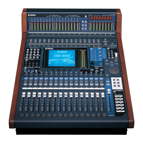
Digital production console/ peak meter bridge/wooden side panels
Hide thumbs
Also See for DM1000:
- Owner's manual (382 pages) ,
- Manual (30 pages) ,
- Startup manual (18 pages)
Table of Contents
Quick Links
PEAK METER BRIDGE/WOODEN SIDE PANELS
This document is printed on chlorine free (ECF) paper with soy ink.
PA
011681
Dm1000: 200303-600000
MB1000: 200303-105000
SP1000: 200303-35000
DIGITAL PRODUCTION CONSOLE/
/MB1000/SP1000
CONTENTS
BLOCK DIAGRAM
OVERALL CONNECTOR CIRCUIT DIAGRAM
SERVICE MANUAL
................................................... 4
.......................................................... 13
.................................. 14
............................................ 46
.................................. 58
....................................... 65
................................................... 103/109
........................................ 143/144
................................... 150
1.329K-6554
DM1000/MB1000/SP1000
............... 23
............................ 28
................................ 47
.................. 115/129
................. 145
.... 146/148
.......... 150
............... 151
............................ 166
HAMAMATSU, JAPAN
Printed in Japan '03.03
1
Table of Contents

Related Manuals for Yamaha DM1000


Summary of Contents for Yamaha DM1000
- Page 1 LSI PIN DESCRIPTION ........ 47 IC BLOCK DIAGRAM ........58 CIRCUIT BOARDS ........65 INSPECTIONS ........... 103/109 DM1000/MB1000 SERVICE CHECK PROGRAM ....115/129 MB1000 TEST PROGRAM ........143/144 INITIALIZING THE DM1000 ....145 TRANSMITTING PARAMETER SETTINGS VIA MIDI (BULK DUMP) ..146/148 CHECKING THE BATTERY AND THE SYSTEM VERSION ..
- Page 2 IMPOR TANT NOTICE This manual has been provided for the use of authorized Yamaha Retailers and their service personnel. It has been assumed that basic service procedures inherent to the industry, and more specifically Yamaha Products, are already known and under- stood by the users, and have therefore not been restated.
- Page 3 DM1000/MB1000/SP1000 LITHIUM BATTERY HANDLING This product uses a lithium battery for memory back-up. WARNING : Lithium batteries are dangerous because they can be exploded by improper handling. Observe the following pre- cautions when handling or replacing lithium batteries. Leave lithium battery replacement to qualified service personnel.
-
Page 4: Specifications
DM1000/MB1000/SP1000 SPECIFICATIONS General Spec Number of scene memories 44.1 kHz, 48 kHz, 88.2 kHz, 96 kHz Internal Sampling Frequency Normal rate: 44.1 kHz–10% to 48 kHz+6% External Double rate: 88.2 kHz–10% to 96 kHz+6% Less than 1.6 ms CH INPUT to OMNI OUT... - Page 5 DM1000/MB1000/SP1000 — Input patch Phase Normal/reverse On/off Gate-type * Key in: 12 ch Group (1–12, 13–24, 25–36, 37–48)/AUX1–8 On/off Comp-type * Key in: self /Stereo Link Pre EQ/pre fader/post fader –96.0 to +12.0 dB (0.1 dB step) Attenuator 4-band PEQ (TYPE1) * On/off 0–43400 samples...
- Page 6 DM1000/MB1000/SP1000 On/off Comp-type * Pre EQ/pre fader/post fader Attenuator –96.0 to +12.0 dB (0.1 dB step) 4-band PEQ * On/off On/off — STEREO Fader 100 mm motorized Balance 127 positions (Left=1–63, Center, Right=1–63) Delay 0–29100 samples Displayed on LCD Peak hold on/off...
- Page 7 DM1000/MB1000/SP1000 100 V, 50/60 Hz 135 W Japan Power Requirements 120 V, 60 Hz 135 W U.S./Canada Other 220–240 V, 50/60 Hz 135 W 200 x 585 x 436 mm (7.8" x 23.0" x 17.1") With MB1000 and SP1000 installed: 295 x 635 x 486 mm (11.6" x 25.0" x...
- Page 8 DM1000/MB1000/SP1000 Comp Parameters –54 dB to 0 dB (0.1 dB step) Threshold x=1, 1.1, 1.3, 1.5, 1.7, 2, 2.5, 3, 3.5, 4, 5, 6, 8, 10, 20, ∞ (16 points) Ratio (x :1) Out gain 0 dB to +18 dB (0.1 dB step)
- Page 9 DM1000/MB1000/SP1000 Libraries Presets 52 (EFFECT 2–4: 44) Effect library (EFFECT 1–4) User memories Presets Compressor library User memories Presets Gate library User memories Presets EQ library User memories Presets Channel library User memories Presets Surround Monitor library User memories Presets...
- Page 10 DM1000/MB1000/SP1000 Digital Input Spec Input Format Data length Level Connector XLR-3-31 type (Balanced) * AES/EBU 24-bit RS422 2TR IN DIGITAL 0.5 Vpp/75 Ω IEC-60958 24-bit Phono 1. XLR-3-31 type connectors are balanced (1=GND, 2=HOT, 3=COLD). Digital Output Spec Output Format...
- Page 11 DM1000/MB1000/SP1000 I/O Slot Spec (1-2) Each I/O SLOT accepts a digital interface card. SLOT #1 has a serial interface. OUTPUT number of Maker Model Function INPUT Format Resolution Frequency Note Available cards Can handle MY8-AT Digital I/O ADAT 20 bit 44.1/48 kHz...
-
Page 12: Control Port
DM1000/MB1000/SP1000 REMOTE Port Signal Signal RX+/GND * RX–/RX– * RTS/RX+ * TX–/TX+ * CTS/TX– * TX+/GND * N.C. 1. RS422 (for AD824)/SONY 9 pin protocol (P2) CONTROL Port Signal Signal GPO0 GPO1 GPO2 GPO3 GPO4 GPO5 GPO6 GPO7 GPI0 GPI1... - Page 13 DM1000/MB1000/SP1000 DIMENSIONS Top view Front view Side view Units: mm With MB1000 and SP1000 installed Top view Front view Side view Units: mm...
-
Page 14: Panel Layout
DM1000/MB1000/SP1000 PANEL LAYOUT DM1000 Control Panel SELECTED CHANNEL Section (p. 18) AD Input Section (p. 15) DISPLAY ACCESS Section (p. 17) Headphones +48V +48V +48V +48V +48V +48V +48V +48V +48V +48V +48V +48V +48V +48V +48V +48V & Talkback Section (p. - Page 15 DM1000/MB1000/SP1000 AD Input Section +48V +48V +48V +48V +48V +48V +48V +48V +48V +48V +48V +48V +48V +48V +48V +48V 20dB 20dB 20dB 20dB 20dB 20dB 20dB 20dB 20dB 20dB 20dB 20dB 20dB 20dB 20dB 20dB GAIN GAIN GAIN GAIN...
- Page 16 DM1000/MB1000/SP1000 STEREO Section AUTO q [AUTO] button w [SEL] button e [ON] button r [STEREO] fader STEREO AUX SELECT Section AUX SELECT DISPLAY q [DISPLAY] button w [AUX 1]–[AUX 8] buttons ENCODER MODE Section ENCODER MODE q [DISPLAY] button DISPLAY...
- Page 17 DM1000/MB1000/SP1000 DISPLAY ACCESS Section q [AUTOMIX] button w [DIO] button e [SETUP] button r [UTILITY] button DISPLAY ACCESS t [MIDI] button y [REMOTE] button AUTOMIX SETUP UTILITY u [METER] button MIDI REMOTE METER VIEW i [VIEW] button o [PAIR/GROUP] button...
- Page 18 DM1000/MB1000/SP1000 SELECTED CHANNEL Section q ROUTING [DISPLAY] button w ROUTING [1]–[8] buttons SELECTED CHANNEL e ROUTING [STEREO] button ROUTING EQUALIZER r ROUTING [DIRECT] button DISPLAY DISPLAY t EQUALIZER [DISPLAY] button HIGH y EQUALIZER [HIGH] button u EQUALIZER [HIGH-MID] button HIGH MID...
- Page 19 DM1000/MB1000/SP1000 USER DEFINED KEYS Section USER DEFINED KEYS DISPLAY q [DISPLAY] button w [1]-[12] buttons Data Entry Section q Parameter wheel w [ENTER] button e [DEC] & [INC] buttons r Left, Right, Up, Down cursor buttons ENTER Headphones & Talkback Section...
-
Page 20: Rear Panel
DM1000/MB1000/SP1000 MONITOR Section q [DISPLAY] button MONITOR w [SOLO] indicator DISPLAY e [CLEAR] button r [2TR D1] button SOLO CLEAR t [2TR D2] button 2TR D2 STEREO 2TR D1 y [STEREO] button u [SLOT] button SLOT i [BUS] button MONITOR... - Page 21 DM1000/MB1000/SP1000 SLOT Section SLOT SLOT q [SLOT 1] & [SLOT 2] Digital I/O & Control Section METER SMPTE IN REMOTE MIDI TO HOST WORD CLOCK 2TR IN DIGITAL CONTROL AES/EBU COAXIAL COAXIAL AES/EBU q [METER] connector w [CONTROL] connector e [SMPTE TIME CODE INPUT] connector r [REMOTE] connector t [MIDI IN &...
- Page 22 DM1000/MB1000/SP1000 MB1000 Controls q Channel indicators w [INPUT METERING POSITION] indicators e [OUTPUT METERING POSITION] indicators r [PEAK HOLD] button t [TIME CODE] display y [1-16] / [17-32] / [33-48] / [REMOTE 1] / [REMOTE 2] / [MASTER] buttons u Level meters...
-
Page 23: Circuit Board Layout
DM1000/MB1000/SP1000 CIRCUIT BOARD LAYOUT DM1000 Bottom AssemblyMAIN Power transformer ... -
Page 24
DM1000/MB1000/SP1000
MAIN Power transformer ... -
Page 25
DM1000/MB1000/SP1000 Rear Assembly U
HAAD HAAD ... -
Page 26
DM1000/MB1000/SP1000 Control Panel Asembly
(1/4) (2/4) (3/4) (4/4) -
Page 27: Table Of Contents
DM1000/MB1000/SP1000 MB1000 Front Panel Assembly Rear Panel AssemblyMAIN... -
Page 28: Disassembly Procedure
(See page 150.) Disassembling the DM1000 Removing the SP1000 (Time required: About 2 minutes) 1-1. If the SP1000 is attached to the DM1000, remove the ten (10) screws marked [A], and then both sides must be removed. (Fig.1) DM1000 SP1000... - Page 29 DM1000/MB1000/SP1000 Rear Assembly U (Time required: About 9 minutes) 4-1. Remove the SP1000. (See procedure 1.) 4-2. Remove the MB1000. (See procedure 2.) 4-3. Fasten the control panel assembly. (See procedure 3.) 4-4. Remove the six (6) screws marked [40A] and the two (2) screws marked [70A].
- Page 30 DM1000/MB1000/SP1000 Bottom Assembly Section DCD Circuit Board (Time required: About 8 minutes) 5-1. Remove the SP1000. (See procedure 1.) 5-2. Remove the MB1000. (See procedure 2.) 5-3. Fasten the control panel assembly. (See procedure 3.) 5-4. Remove the four (4) screws marked [410] and the two (2) screws marked [411].
- Page 31 DM1000/MB1000/SP1000 MAIN Circuit Board (Time required: About 12 minutes) 9-1. Remove the SP1000. (See procedure 1.) 9-2. Remove the MB1000. (See procedure 2.) 9-3. Fasten the control panel assembly. (See procedure 3.) 9-4. Remove the rear assembly U. (See procedure 4-5.) 9-5.
-
Page 32
DM1000/MB1000/SP1000
[341] [335] OPT angle Bottom stay DCA 1/5 [230] Photo.5 Photo.7 Photo.6 Heat sink DCAIC angle Bottom stay [12B] OPT angle [12B] [340] [411] Photo.4 [410] IF plate ... -
Page 33
DM1000/MB1000/SP1000
[130A] AC shield plate MAIN [285] [12C] [60B] Power transformer Lithium Battery Battery VN103500 VN103600(Battery holder for VN103500) Notice for back-up battery removal Push the battery as shown in figure, then the battery will pop up. Druk de batterij naar beneden zoals aangeven in de tekening de batterij springt dan naar voren. - Page 34 DM1000/MB1000/SP1000 AC Shield Plate (Time required: About 10 minutes) 13-1. Remove the SP1000. (See procedure 1.) 13-2. Remove the MB1000. (See procedure 2.) 13-3. Fasten the control panel assembly. (See procedure 3.) 13-4. Fasten the rear assembly U. (See procedure 4-4.) 13-5.
- Page 35 DM1000/MB1000/SP1000 [265]: Cord holder (underneath the ferrite core) [255] Locking card spacer Ferrite core [290A] Power switch knob [255]: Bind Head Tapping Screw-B 3.0X6 MFZN2BL (EP600230) Photo.9 [290A]: Bind Head Tapping Screw-S 4.0X8 MFZN2BL (VI693100) Photo.8 [290B] [290B]: Bind Head Tapping Screw-S 4.0X8 MFZN2BL (VI693100)
- Page 36 DM1000/MB1000/SP1000 Rear Assembly U Section ADA Circuit Board (Time required: About 10 minutes) 17-1. Remove the SP1000. (See procedure 1.) 17-2. Remove the MB1000. (See procedure 2.) 17-3. Fasten the control panel assembly. (See procedure 3.) 17-4. Fasten the rear assembly U. (See procedure 4-4.) 17-5.
-
Page 37
DM1000/MB1000/SP1000
[120A] [120A] [120A] [120A] [120A] [120A] [120A] [120A] [120A] [110B] [130B] [130B] [120A] [120A] [110B] [110B] [110B] [110B] [110B] [110B] [130B] [130B] [130B] [180] [190] [180] Knob x18 PC support Headt sink HAAD HAAD [240A] [110B]: Bonding Tapping Screw-B 3.0X8 MFZN2BL (VN413300) - Page 38 DM1000/MB1000/SP1000 Heat Sink (Time required: About 8 minutes) 19-1. Remove the SP1000. (See procedure 1.) 19-2. Remove the MB1000. (See procedure 2.) 19-3. Fasten the control panel assembly. (See procedure 3.) 19-4. Remove the two (2) screws marked [70A]. (Fig.2) 19-5.
-
Page 39
DM1000/MB1000/SP1000
HAAD HAAD HAAD Button assembly x16 Knob spacer x18 Photo.13 [60C]: Bind Head Tapping Screw-B 3.0X8 MFZN2BL (EP600190) Fig.7 [60C] Control Panel Assembly Section When removing the circuit board, if it is hard to handle while the control panel assembly is fixed slantwise at the stay, open it widely at 180°... - Page 40 DM1000/MB1000/SP1000 LCD Circuit Board (Time required: About 8 minutes) 24-1. Remove the SP1000. (See procedure 1.) 24-2. Remove the MB1000. (See procedure 2.) 24-3. Fasten the control panel assembly. (See procedure 3.) 24-4. Remove the two (2) screws marked [120B] and the two (2) screws marked [170].
-
Page 41
DM1000/MB1000/SP1000
[300]: Encoder knob [350B]: Knob [310]: Encoder knob x16 Encoder knob Fader knob x17 Fig.8... -
Page 42
DM1000/MB1000/SP1000
[120D] [220B] (1/4) (1/4) (2/4 Meter) [220B] (3/4 Joystick) [220B] [218] [220A] (4/4 Encoder) Encoder angle bracket Cord holder [220A] Cord holder [220B] Insulation sheet [240B] Cord holder Cord holder [260] Encoder angle bracket [120B]: Bind Head Tapping Screw-B 3.0X8 MFZN2BL (EP600190) - Page 43 DM1000/MB1000/SP1000 (Time required: About 10 minutes) 27-1. Remove the SP1000. (See procedure 1.) 27-2. Remove the MB1000. (See procedure 2.) 27-3. Fasten the control panel assembly. (See procedure 3.) 27-4. Remove the LCD shield plate. (See procedure 24-4.) 27-5. Remove the PN1 (2/4 meter) circuit board.
- Page 44 DM1000/MB1000/SP1000 Disassembling the MB1000 Rear Panel (Time required: About 3 minutes) 28-1. Remove the MB1000. (See procedure 2.) 28-2. Remove the sixteen (16) screws marked [40C]. The rear panel can then be removed from the front panel. (Fig.10) PN Circuit Board (Time required: About 4 minutes) 29-1.
-
Page 45
DM1000/MB1000/SP1000 Front panel
[40C] [40C] [40C] Rear panel [40C]: Bind Head Tapping Screw-B 3.0X8 MFZN2BL (EP600190) Fig.10 [50] Cable holder [70C] MAIN [70B] Meter angle L... -
Page 46: Installing An Optional Card
INSTALLING AN OPTIONAL CARD Follow the steps below to install an optional mini-YGDAI card. 1 Make sure that the power to the DM1000 is turned off. 2 Undo the two fixing screws and remove the slot cover, as shown below. -
Page 47: Lsi Pin Description
DM1000/MB1000/SP1000 LSI PIN DESCRIPTION DM1000 M37641M8-141FP (X2485200) CPU (USB 32K) ................47 HD6417709SF133 (X2081A00) CPU (SH-3) ................. 48 SH7042 (X4409A00) CPU (SUB) ....................49 MBCG46183-129PFV-G (XV833A00) Gate Array (SIO4) ............50 SGH603064F-62F (XV973A00) Gate Array .................. 50 YSS910-S (XV988A00) DSP6 (Digital Signal Processor) ............51 YSS919B-H (XZ693B00) DSP7 (Digital Signal Processor) ............ - Page 48 DM1000/MB1000/SP1000 HD6417709SF133 (X2081A00) CPU (SH3) MAIN: IC001 NAME FUNCTION NAME FUNCTION CKE/PTK5 CK enable / Port K Mode control RAS3L/PTJ0 RAS address bus / Port J Vcc(RTC) Power supply +1.8 V PTJ1 Port J XTAL2 CASL/PTJ2 CAS address bus / Port J...
- Page 49 DM1000/MB1000/SP1000 SH7042 (X4409A00) CPU (SUB) FD: IC203 NAME FUNCTION NAME FUNCTION PE14 Port E PE15 Data bus Ground Ground Data bus Power supply +5V Address bus Data bus Ground XTAL Crystal oscillator Mode control EXTAL Crystal oscillator Mode control Non-maskable interrupt request...
- Page 50 DM1000/MB1000/SP1000 MBCG46183-129PFV-G (XV833A00) Gate Array (SIO4) MAIN: IC651 NAME FUNCTION NAME FUNCTION TX31 Transmit Data 31 Data Bus RX32 Receive Data 32 TX32 Transmit Data 32 /IRQ0 Interrupt Request Port 0 RX33 Receive Data 33 /IRQ1 Interrupt Request Port 1...
- Page 51 DM1000/MB1000/SP1000 YSS910-S (XV988A00) DSP6 (Digital Signal Processor) MAIN: IC301-304 NAME FUNCTION NAME FUNCTION Power supply (3.3 V) Ground Ground DB13 System master clock input (60 MHz or 30 MHz) DB14 System master clock output (High or 30 MHz) DB15 Vdd5...
- Page 52 DM1000/MB1000/SP1000 YSS919-H (XZ693A00) DSP7 (Digital Signal Processor) MAIN: IC201-206 NAME FUNCTION NAME FUNCTION PLLEN PLL enable input (0: PLL unuse, 1: PLL use) SIO32 /TEST Test mode setting (0: TEST, 1: Normal) SIO33 AVss Analog ground SIO34 PLL filter SIO35...
- Page 53 DM1000/MB1000/SP1000 MBCG61594-130 (X3299A00) ATSC2A MAIN: IC501, 502 NAME FUNCTION NAME FUNCTION Power supply +3.3V Power supply +3.3V XTST LSI test pin PB_H_M4_SEL Port B audio data input buffer active select Ground PB_O_MUTE Port B mute WT_X CPU interface write input...
- Page 54 DM1000/MB1000/SP1000 YM3436DK (XG948E0) DIR2 (Digital Format Interface Receiver) MAIN: IC144 NAME FUNCTION NAME FUNCTION DAUX Auxiliary input for audio data RSTN System reset input HDLT Asynchronous buffer operation flag Vdda VCO section power (+5V) DOUT Audio data output CTLN VCO control input N...
- Page 55 DM1000/MB1000/SP1000 S1D13704F00A100 (X3498A00) LCDC (LCD Controller) MAIN: IC027 NAME FUNCTION NAME FUNCTION COREV Power supply +3.3V COREV Power supply +3.3V /WAIT Wait signal DRDY TFT/D-TFD display enable DB15 LCDPWR LCD power control DB14 TESTEN Test enable input DB13 CNF4 DB12...
- Page 56 DM1000/MB1000/SP1000 ICS2008BV-T (X2832B00) T.C. Reader/Generator JK1: IC254 NAME FUNCTION NAME FUNCTION INTR Interrupt request Clear to send RESET Master reset UART transmit data FRAME Color frame A / B input Ready to send CLICK LTC SYNC input LRCLK SMPTE LTC receive clock...
- Page 57 DM1000/MB1000/SP1000 MB1000 SH7042 (X4409A00) CPU (SH-2) MAIN: IC106 NAME FUNCTION NAME FUNCTION PE14 Port E PE15 Data bus Ground Ground Data bus Power supply +5V Address bus Data bus Ground XTAL Crystal oscillator Mode control EXTAL Crystal oscillator Mode control...
-
Page 58: Ic Block Diagram
DM1000/MB1000/SP1000 IC BLOCK DIAGRAM DM1000 TC74VHC00F (XT229A00) HD74LV02AFPEL (IS000200) TC74VHC04F-EL (XM332A00) MAIN: IC138 MAIN: IC020-022 MAIN: IC131 Quad 2 Input NOR Hex Inverter SN74HC00NSR (XE165A00) FD: IC106 Quad 2 Input NAND TC74VHC08F (XT014A00) TC74VHC11F (EL) (XT812A00) TC74VHC14F-EL (XW876A00) MAIN: IC604... - Page 59 DM1000/MB1000/SP1000 TC74VHC138F (XT015A00) TC74VHC157F (EL) (XT475A00) HD74HC123AP (IR012310) FD: IC301, 401, 501 MAIN: IC503-506 DCA: IC350 3 to 8 Demultiplexer Quad 2 to 1 Multiplexer Dual Retriggerable Single Shot SELECT 1 Rext / Cext Select STROBE Cext Output Enable 2 Cext...
- Page 60 DM1000/MB1000/SP1000 74VHC245SJX (XY874A00) HD74LV574AFPEL (IS057400) HD74HC4051FPEL (XP373A00) SN74LV574ANSR (IS057410) ADA: ICIC955, 956 FD: IC110, 114, 120, 603, 604, 609 HAAD: IC952, 953 Single 8-channel FD: IC602 TC74HC245AF (XS720A00) Multiplexer/Demultiplexer Octal D-Type Flip-Flop FD: IC404, 405, 408 TC74VHC245F (XT487A00) Output MAIN: IC102-106, 113-116, 132, 133,...
- Page 61 DM1000/MB1000/SP1000 SN75C1168NSR (XU073A00) DS26C32ATMX (XU815A00) TC7S04F (XM182A00) JK1: IC203 JK1: IC001 ADA: IC954 JK2: IC701 HAAD: IC951 Quad Differential Line Receiver Line Driver/Receiver Inverter Gate INPUT A INPUT A INPUT B OUTPUT A INPUT B ENABLE OUTPUT B OUTPUT C...
- Page 62 DM1000/MB1000/SP1000 CY2305 (XY937A00) MAIN: IC003 Clock Buffer Block Diagram CLKOUT Pin No. Signal Function CLKA1 Input reference frequency, 5V-tolerant input CLK OUT CLKA2 CLK2 Buffered clock output CLK2 CLK4 CLK1 Buffered clock output CLKA3 Ground CLK1 CLKA4 CLK3 Buffered clock output 3.3V supply...
- Page 63 DM1000/MB1000/SP1000 TLC2932IPWR (XV064A00) MAIN: IC143 LOGIC V PFD INHIBIT VCO INHBIT VCO V VCO OUT SELECT LOGIC V VCO V DETECTOR CHARGE PUMP SELECT BIAS VCO OUT COIN VCO GND VCO INHBIT PFD OUT PFD INHIBIT LOGIC GND LOGIC GND...
- Page 64 DM1000/MB1000/SP1000 MB1000 TC74HC238AF (XT163A00) MAIN: IC109 3 to 8 Line Decoder Select Inputs Enable Data Inputs Output TC74HC245AF (XS720A00) SN75C1168N SR (XU073A00) TD62M8600F (XV014A00) MAIN: IC108 MAIN: IC103 PN: IC202, 206 PN: IC201 Line Driver/Receiver Source Driver Octal 3-State Bus Transceiver...
-
Page 65: Circuit Boards
DM1000/MB1000/SP1000 CIRCUIT BOARDS DM1000 DCCOM (AC) Circuit Board (X3434C0) ........66 DCCOM (DCA 1/5) Circuit Board (X3434C0) ....... 67 DCCOM (DCA 2/5) Circuit Board (X3434C0) ....... 66 DCCOM (DCA 3/5) Circuit Board (X3434C0) ....... 66 DCCOM (DCA 4/5) Circuit Board (X3434C0) ....... 66 DCD Circuit Board (X3858B0) .......... - Page 66 DM1000/MB1000/SP1000 POWER ON/OFF DCCOM (AC) Circuit Board to AC Inlet Assembly to Power Transformer to Bottom Chassis (for ground) Component side DCCOM (DCA 2/5) Circuit Board DCCOM (DCA 3/5) Circuit Board to DCA 1/5-IC302 to DCA 1/5-IC301 Component side Component side...
- Page 67 DM1000/MB1000/SP1000 DCCOM (DCA 1/5) Circuit Board to DCA 4/5 -CN403 to DCA 3/5 -CN402 to FD-CN202 to DCA 2/5 -CN401 Power Transformer to HAAD 1/2 -CN952 to ADA -CN954 to OPT -CN807 to JK1-CN653 Component side 2NAP-V990110-2 (J, U, V models)
- Page 68 DM1000/MB1000/SP1000 DCD Circuit Board to MAIN-CN006 not installed to FD-CN201 to PN1 (1/4)-CN105 Power Transformer Component side 2NAP-V990130-2...
- Page 69 DM1000/MB1000/SP1000 DCD Circuit Board Pattern side 2NAP-V990130-2...
- Page 70 DM1000/MB1000/SP1000 FD Circuit Board to MAIN-CN003 to PN1 (1/4)-CN101 to PN1 (1/4)-CN102 installed 1 fader 2 fader 3 fader 4 fader 5 fader 6 fader 7 fader 8 fader 9 fader 2NAP-V989990-2...
- Page 71 DM1000/MB1000/SP1000 to DCA 1/5-CN306 to PN1 (1/4)-CN104 to PN1 (1/4)-CN103 to DCD-CN202 fader 10 fader 11 fader 12 fader 13 fader 14 fader 15 fader 16 fader STEREO fader Component side 2NAP-V989990-2...
- Page 72 DM1000/MB1000/SP1000 FD Circuit Board to DCA 1/5-CN306 to PN1 (1/4)-CN104 to DCD-CN202 to PN1 (1/4)-CN103 2NAP-V989990-3...
- Page 73 DM1000/MB1000/SP1000 to PN1 (1/4)-CN102 to PN1 (1/4)-CN101 to MAIN-CN003 installed Pattern side 2NAP-V989990-3...
- Page 74 DM1000/MB1000/SP1000 HACOM (ADA) Circuit Board to MAIN-CN901 to XLR-CN151 to XLR-CN551 HACOM (ADA) Circuit Board 2NAP-V989910-2 2NAP-V989910-3...
- Page 75 DM1000/MB1000/SP1000 to DCA 1/5-CN305 to XLR-CN951 to XLR-CND51 Component side Pattern side 2NAP-V989910-2 2NAP-V989910-3...
- Page 76 DM1000/MB1000/SP1000 HACOM (HAAD 1/2) Circuit Board to XLR-CN101 to XLR-CN501 PAD 20dB 1 PAD 20dB 2 PAD 20dB 3 PAD 20dB 4 PAD 20dB 5 PAD 20dB 6 PAD 20dB 7 PAD 20dB 8 PAD 20dB 9 PAD 20dB 10...
- Page 77 DM1000/MB1000/SP1000 to XLR-CN901 to XLR-CND01 20dB 10 PAD 20dB 11 PAD 20dB 12 PAD 20dB 13 PAD 20dB 14 PAD 20dB 15 PAD 20dB 16 TALKBACK LEVEL to HAAD 2/2 -CN003 PHONES GAIN 10 GAIN 11 GAIN 12 GAIN 13...
- Page 78 DM1000/MB1000/SP1000 HACOM (HAAD 1/2) Circuit Board HACOM (HAAD 2/2) Circuit Board 2NAP-V989910-3 Pattern side...
- Page 79 DM1000/MB1000/SP1000 Pattern side 2NAP-V989910-3...
- Page 80 DM1000/MB1000/SP1000 JKCOM (JK1) Circuit Board to DCA 1/5-CN307 to MAIN-CN651 SMPTE IN MIDI IN/OUT REMOTE CONTROL to MAIN-CN652 TO HOST USB AES/EBU AES/EBU COAX WORD CLOCK 2TR IN/OUT DIGITAL JKCOM (JK2) Circuit Board Component side to MAIN-CN701 Component side 2NAP-V989800-2...
- Page 81 DM1000/MB1000/SP1000 JKCOM (JK1) Circuit Board Pattern side JKCOM (JK2) Circuit Board Pattern side 2NAP-V989800-2...
- Page 82 DM1000/MB1000/SP1000 JKCOM (OPT) Circuit Board to MAIN-CN801 SLOT1 to MAIN-CN802 to DCA 1/5-CN302 to MAIN-CN803 SLOT2 to MAIN-CN804 Component side 2NAP-V989800-2...
- Page 83 DM1000/MB1000/SP1000 JKCOM (OPT) Circuit Board Pattern side 2NAP-V989800-2...
- Page 84 DM1000/MB1000/SP1000 MAIN Circuit Board to FD-CN203 not used (for check) to LCD -CN501 to DCD-CN203 to HAAD 1/2-CN951 to ADA-CN953 Lithium Battery Battery VN103500 VN103600(Battery holder for VN103500) Notice for back-up battery removal Battery Push the battery as shown in figure, then the battery will pop up.
- Page 85 DM1000/MB1000/SP1000 to OPT-CN802 to OPT -CN801 to JK1 -CN652 to JK1 -CN651 to JK2 -CN701 to OPT-CN804 to OPT-CN803 Component side 2NAP-V989750-2...
- Page 86 DM1000/MB1000/SP1000 MAIN Circuit Board 2NAP-V989750-2...
- Page 87 DM1000/MB1000/SP1000 Component side 2 layer 2NAP-V989750-2...
- Page 88 DM1000/MB1000/SP1000 MAIN Circuit Board 2NAP-V989750-2...
- Page 89 DM1000/MB1000/SP1000 Component side 5 layer 2NAP-V989750-2...
- Page 90 DM1000/MB1000/SP1000 MAIN Circuit Board 2NAP-V989750-3...
- Page 91 DM1000/MB1000/SP1000 Pattern side 2NAP-V989750-3...
- Page 92 DM1000/MB1000/SP1000 PNCOM (PN1 (1/4)) Circuit Board to FD-CN403 to FD-CN404 2NAP-V990000-2...
- Page 93 DM1000/MB1000/SP1000 to PN1 (2/4)-CN401 to PN1 (3/4)-CN109 to PN1 (4/4) -CN111 to DCD -CN204 to PN2 -CN301 to FD-CN401 to FD-CN402 Component side 2NAP-V990000-2...
- Page 94 DM1000/MB1000/SP1000 PNCOM (PN1 (1/4)) Circuit Board 2NAP-V990000-2...
- Page 95 DM1000/MB1000/SP1000 Pattern side 2NAP-V990000-2...
- Page 96 DM1000/MB1000/SP1000 PNCOM (PN1 (2/4)) Circuit Board LCD contrast Component side to LCD-CN503 to PN1 (1/4)-CN107 Pattern side PNCOM (PN1 (3/4)) Circuit Board PNCOM (PN1 (4/4)) Circuit Board Parameter wheel Component side Pattern side Joy stick Component side Pattern side PNCOM (PN2) Circuit Board...
- Page 97 DM1000/MB1000/SP1000 PNCOM (LCD) Circuit Board LCD Module LCD Module to PN1 (2/4)-CN402 to MAIN-CN005 Component side Pattern side 2NAP-V990000-2...
- Page 98 DM1000/MB1000/SP1000 XLR Circuit Board to HAAD 1/2-CND02 to HAAD 1/2-CN902 +48V ON/OFF +48V ON/OFF +48V ON/OFF +48V ON/OFF +48V ON/OFF +48V ON/OFF +48V ON/OFF 10 +48V ON/OFF 9 INPUT INPUT INPUT INPUT INPUT INPUT INPUT INPUT OMNI IN OMNI IN...
- Page 99 DM1000/MB1000/SP1000 MAIN Circuit Board to PN-CN201 installed to METER (DM1000) Component side 2NAP-V990400-2...
- Page 100 DM1000/MB1000/SP1000 MAIN Circuit Board Pattern side 2NAP-V990400-2...
- Page 101 DM1000/MB1000/SP1000 PN Circuit Board to MAIN-CN102 Component side 2NAP-V990410-2...
- Page 102 DM1000/MB1000/SP1000 PN Circuit Board Pattern side 2NAP-V990410-2...
- Page 103 DM1000/MB1000/SP1000 INSPECTIONS Perform the Check of DM1000. 1-4. Fader Inspection 1. Preparations q Preparations 1-1. Parameters a. Press the LAYER [MASTER] key to select the The parameters are as follows unless otherwise master layer. specified. b. Move all the faders all the way up.
- Page 104 DM1000/MB1000/SP1000 e Residual noise (OMNI OUT 1~12) y Crosstalk between left and right Parameter Switch BUS OUT Off. Parameter PAN L swung to cut off. Permissible range Input frequency Output level (L) Permitted range (R) -86dBu or below 1kHz -10dBu...
- Page 105 DM1000/MB1000/SP1000 e Distortion ratio (CH 1~16) 2-5. CH IN 1~16 level meter operation check Parameters Input the regulated level to the Input frequency Output level Permissible range channels being measured. 1kHz +22dBu 0.02% or below 1~16 CH can be input at the same time.
- Page 106 DM1000/MB1000/SP1000 3-3. OMNI IN 1~4 4-2. 2TR DIGITAL IN 1, 2 Parameters Inspect with OMNI OUT 1. Parameters Use Parameter System Two. q Distortion ratio (OMNI IN 1~4) For distortion measurement, select BW: 80kHz. Input frequency Output level Permissible range Inspect with OMNI OUT 1 and 2.
- Page 107 DM1000/MB1000/SP1000 4-3. WORD CLOCK IN, 2TR DIGITAL IN 1 and 2 PLL 5-2. WORD CLOCK EXT operation range Parameters Select the WORD CLOCK as follows. Parameters Use Parameter System Two. WORD CLOCK IN inspection: For distortion measurement, select WC IN BW: 80kHz.
- Page 108 [ENTER] switch. Set the CH 1~16 Fader to 10 dB Adjust CH1-16 +10dB 1) Connect the PC and the DM1000 with the USB and the STEREO Fader to 0 dB, STEREO 0dB cable. then press the [ENTER] switch.
- Page 109 DM1000/MB1000/SP1000...
- Page 110 DM1000/MB1000/SP1000...
- Page 111 DM1000/MB1000/SP1000...
- Page 112 DM1000/MB1000/SP1000...
- Page 113 DM1000/MB1000/SP1000...
- Page 114 DM1000/MB1000/SP1000...
-
Page 115: Dm1000/Mb1000 Service Check Program
DM1000/MB1000/SP1000 DM1000/MB1000 SERVICE CHECK PROGRAM Execute the Service Check Program for DM1000 and MB1000. (Fig. 3) Outline Example B of individual check screen (when checking each 0-1. Operation method one of multiple items automatically or visually) Keys used for the service check on the panel... - Page 116 The voltage of the backup battery by A/D display the dialog box for confirmation. Select Yes is measured and judgment is automatic. and press the [ENTER] key to restart the DM1000 in the service check mode. Example of execution screen...
- Page 117 DM1000/MB1000/SP1000 DSP6 test items DSP7 test items 1-13. WORD CLOCK test WORD CLOCK OUT → IN is counted by 1: CPU Interface (Data bus) 1: CPU Interface (Data Bus) Contents: 2: CPU Interface (Data bus) 2: CPU Interface (Chip Select)
- Page 118 DM1000/MB1000/SP1000 1-22. PANEL LED test 1-24. PANEL SW test Contents: Visually check that the 7-segment LEDs Contents: Check that all of the switches on the panel and LEDs on the panel light in the specified respond when pressed in the specified order.
- Page 119 DM1000/MB1000/SP1000 • Move all of the FADERs to the set positions 2) Explanation of the automatic judgment display of the (three positions) and the stop positions will FADER Up/Down be checked and whether or not the values “NG: CH 1, 1020, (990...1023), 980”...
- Page 120 DM1000/MB1000/SP1000 Example of execution screen 1-32. METER SW test Contents: Check that the corresponding LEDs light/ If the judgment is OK or NG, turn off when the MB1000 SWs are the test continues with the check pressed. of the next channel automatically.
- Page 121 DM1000/MB1000/SP1000 2. Supplement LCD display Fig. 1 Panel SW operation order screen (See SW operation Fig. 1 and 2 for operation order.) LCD display: 53 columns × 30 lines (320 × 240 dots with Font 5×7) The [DEC] SW is not displayed during the 1-24.
- Page 122 DM1000/MB1000/SP1000 SW operation Fig. 1 GROUP 1 SW operation Fig. 2 GROUP 2...
- Page 123 DM1000/MB1000/SP1000 LED lighting order Fig. 1 LED lighting order Fig. 2...
- Page 124 Startup method While pressing the [AUX SELECT DISPLAY] and 3-1. Outline [AUX5] keys, turn the power ON. Execute the Audio Check for DM1000. Limits • Possible operation keys are for the DATA ENTRY Check method SECTION only.
- Page 125 DM1000/MB1000/SP1000 MODE Changing the input/output terminals ANALOG Patches the ANALOG I/O to the input/output. SLOT 1 Patches the SLOT 1 I/O to the input/output. SLOT 2 Patches the SLOT 2 I/O to the input/output. 2TRD Patches the 2TRD 1, 2 I/O to the input/output.
- Page 126 DM1000/MB1000/SP1000 CH20 OMNI4 CH21 INPUT1 CH22 INPUT2 CH23 INPUT3 CH24 INPUT4 CH25 INPUT5 CH26 INPUT6 CH27 INPUT7 CH28 INPUT8 CH29 INPUT9 CH30 INPUT10 CH31 INPUT11 CH32 INPUT12 CH33 INPUT13 CH34 INPUT14 CH35 INPUT15 CH36 INPUT16 CH37 OMNI1 CH38 OMNI2 CH39...
- Page 127 DM1000/MB1000/SP1000 CH30 SLOT1-14 CH31 SLOT1-15 CH32 SLOT1-16 CH33 SLOT1-1 CH34 SLOT1-2 CH35 SLOT1-3 CH36 SLOT1-4 CH37 SLOT1-5 CH38 SLOT1-6 CH39 SLOT1-7 CH40 SLOT1-8 CH41 SLOT1-9 CH42 SLOT1-10 CH43 SLOT1-11 CH44 SLOT1-12 CH45 SLOT1-13 CH46 SLOT1-14 CH47 SLOT1-15 CH48 SLOT1-16 Mode: Patch setting during SLOT2...
- Page 128 DM1000/MB1000/SP1000 CH40 SLOT2-8 CH41 SLOT2-9 CH42 SLOT2-10 CH43 SLOT2-11 CH44 SLOT2-12 CH45 SLOT2-13 CH46 SLOT2-14 CH47 SLOT2-15 CH48 SLOT2-16 MODE: Patch setting during 2TRD INPUT CH IN PORT OUTPUT CH(BUS/AUX) OUT PORT 2TRD1L BUS1 2TRD1L 2TRD1R BUS2 2TRD1R 2TRD2L BUS3...
- Page 129 --- PANEL ALL LED --- 1 BRIGHTNESS NG 2 RED LEDs OK 3 GREEN LEDs OK 4 ORANGE LEDs EXIT ([DEC] Key->[ENTER] Key) --- DM1000 test --- (C)YAMAHA 2003 F/W Ver. MAIN Vx.xx METER Vx.xx SUB1 Vx.xx PLLP2 OK 22 PANEL LED...
- Page 130 DM1000/MB1000/SP1000 --- PLLP2 --- Adrs,Data BUS EXIT ([DEC] Key->[ENTER] Key) --- BATT --- DM1000 2TR IN DIGITAL1 2TR IN DIGITAL2 BATT NG:BATT (2.56V) 2TR OUT DIGITAL1 2TR OUT DIGITAL2 EXIT ([DEC Key]->[ENTER Key]) WORD CLOCK IN WORD CLOCK OUT TO HOST-USB...
- Page 131 DM1000/MB1000/SP1000 → → → → → → → --- WORD CLOCK --- ... NG: IC201 Interface (Data Bus) OUT->IN 0000 0000 XXXX 0000 0000 0000 0000 X00X NG PLL (DIR2,DBL) NG PLL UnLock Connection (DSP7 → DSP6) Disconnect BNC cable 1 IC201 S0[xx] →...
- Page 132 DM1000/MB1000/SP1000 --- PANEL LED --- 1 CH1...CH16 PEAK-SIGNAL OK 2 AUX SELECT..FADER MODE OK 3 CH1..CH16 SEL-SOLO-ON, STEREO AUTO-SEL-ON OK 4 ROUTING..SCENE MEMORY OK 5 MONITOR OK 6 LAYER..USER DEFINED KEYS OK 7 STEREO METER OK 8 ALL LED ON...
- Page 133 DM1000/MB1000/SP1000 --- FADER Move --- 1 FADER Up Position OK 2 FADER Down Position OK 3 FADER Up NG 4 FADER Down OK 5 FADER Position1 OK 6 FADER Position2 OK 7 FADER Position3 [ENTER] key to Start FADER Up EXIT ([DEC] Key->[ENTER] Key)
- Page 134 DM1000/MB1000/SP1000 --- MESSAGE LOG --- [ 2 BATT] NG:BATT (2.56V) [ 6 MIDI] OK: SCI2 BACK:[UP] NEXT:[DOWN] EXIT:[ENTER] Page...
- Page 135 DM1000/MB1000/SP1000...
- Page 136 DM1000/MB1000/SP1000...
- Page 137 DM1000/MB1000/SP1000...
- Page 138 DM1000/MB1000/SP1000 DM1000 Audio Check (c) YAMAHA2003 MODE CLOCK ANALOG SLOT1 SLOT2 2TRD INT 48k INT 48k INPUT DSP7-1 DSP7-2 IN PORT IC103 IC201 IC202 INPUT1 16, 17 DSP7-3 DSP7-4 DSP7-5 DSP7-6 IC203 IC204 IC205 IC206 PHONE BUS1 DSP7-5 DSP7-6 DSP7-5...
- Page 139 DM1000/MB1000/SP1000...
- Page 140 DM1000/MB1000/SP1000...
- Page 141 DM1000/MB1000/SP1000...
- Page 142 DM1000/MB1000/SP1000...
-
Page 143: Mb1000 Test Program
Preparation 1) Connect the D-sub 15-pin cable to the [METER] terminal on the rear of the DM1000. 2) If there is no DM1000, supply +16.5 V power with an external power supply to the +12V terminal and the ground terminal. - Page 144 DM1000/MB1000/SP1000...
-
Page 145: Initializing The Dm
• You can also store the data to an external MIDI device, such as a MIDI data filer, by using MIDI Bulk Dump. (See page 146.) 1 Make sure that the power to the DM1000 is turned off. 2 While holding down the SCENE MEMORY [STORE] button, turn on the POWER ON/OFF switch. -
Page 146: Transmitting Parameter Settings Via Midi (Bulk Dump)
TRANSMITTING PARAMETER SETTINGS VIA MIDI (BULK DUMP) You can back up data stored in the DM1000, such as libraries and Scenes, to an external MIDI device by using MIDI Bulk Dump. In this way, you can later restore previous DM1000 settings by transmitting this MIDI data back to the DM1000. - Page 147 Note: Data selected by the SETUPMEM button includes MIDI transmission and reception port settings and message settings. After you store to an external device bulk dump data that has its reception disabled, if the DM1000 later starts to receive this particular data, DM1000 bulk dump reception will be turned off immediately, and the DM1000 will be unable to receive subsequent data.
- Page 148 DM1000/MB1000/SP1000...
- Page 149 DM1000/MB1000/SP1000...
-
Page 150: Checking The Battery And The System Version
You can correct the shifted faders using the Calibration function. 1 Make sure that the power to the DM1000 is turned off. 2 While holding down the [ENTER] button, turn on the POWER ON/OFF switch. -
Page 151: Midi Data Format
127 (7F) Active sense Command rx/tx function * ‘tx’ indicates that the data can be transmitted from the DM1000, and F0 7F dd 06 … F7 MMC MMC command ‘rx’ indicates that the data can be received by the DM1000. COMMAND F0 7F dd 07 …... -
Page 152: Program Change
However if [OMNI] is ON, they will be received regardless of the These messages are transmitted when the Machine Control section of the channel. When a message is received, a Scene Memory will be recalled according DM1000 is operated. to the settings of the [Program Change Table]. Transmission 2.12.2 BULK DUMP... - Page 153 2.12.2.3 Setup memory bulk dump format words of 7-bit data. Of the setup memory of the DM1000, this bulk-dumps data other than the User Conversion from actual data into bulk data define layer, User define plug-in, User define keys, Control change table, and d[0~6]: actual data Program change table.
- Page 154 0bbbbbbb bb System exclusive message STATUS 11110000 F0 total block number(minimum number is 0) BLOCK INFO. 0ttttttt tt Manufacture’s ID number (YAMAHA) ID No. 01000011 43 current block number(0-total block number) 0bbbbbbb bb n=0-15 (Device number=MIDI Channel) SUB STATUS 0010nnnn 2n User define layer data of block[bb]...
- Page 155 256 and following are data for the corresponding channel of the edit buffer. ee=(Invert(‘L’+…+de)+1)&0x7F CHECK SUM 0eeeeeee ee For reception by the DM1000, only the user area is valid. (40-199, 256-) End of exclusive 11110111 F7 System exclusive message STATUS 11110000 F0 Manufacture’s ID number (YAMAHA)
- Page 156 256 and following are data for the corresponding channel of the edit buffer. current block number(0-total block number) 0bbbbbbb bb For reception by the DM1000, only the user area is valid. (36-127, 256-) GATE Library data of block[bb] DATA 0ddddddd ds...
- Page 157 0:Library no.0 – 32:Library no.32, 256:current input patch data, 8192:UNDO Manufacture’s ID number (YAMAHA) ID No. 01000011 43 For reception by the DM1000, only the user area is valid. (1-32, 256, 8192) n=0-15 (Device number=MIDI Channel) SUB STATUS 0010nnnn 2n System exclusive message...
- Page 158 The second and third bytes of the DATA NAME indicate the library number. ‘C’ 0:Library no.0 – 32:Library no.32, 256:current data, 8192:UNDO 01000011 43 For reception by the DM1000, only the user area is valid. (1-32, 256, 8192) ‘9’ 00111001 39 ‘1’...
- Page 159 System exclusive message BLOCK INFO. 0bbbbbbb bh STATUS 11110000 F0 0bbbbbbb bl Manufacture’s ID number (YAMAHA) ID No. 01000011 43 total block number(minimum number is 0) 0ttttttt th n=0-15 (Device number=MIDI Channel) SUB STATUS 0000nnnn 0n 0ttttttt tl FORMAT No.
- Page 160 2.12.3.1.2 Parameter Change basic format (Universal 2.12.3.3 Parameter request (Edit buffer) format) System exclusive message STATUS 11110000 F0 System exclusive message Manufacture’s ID number (YAMAHA) STATUS 11110000 F0 ID No. 01000011 43 Manufacture’s ID number (YAMAHA) n=0-15 (Device number=MIDI Channel) ID No.
- Page 161 (such as bulk re- ception) Reception (only transmitted by the DM1000) This message is echoed if [Parameter change ECHO] is ON. Data received from a port that is assigned to [Cascade Link] and whose Device 2.12.3.12.1 Parameter change (Function call response:...
- Page 162 When the title is changed on the DM1000, this message will be transmitted with Transmission the device number set to [Tx CH]. When a memory or library is cleared on the DM1000, this message will be trans- mitted with the device number set to [Tx CH]. STATUS...
- Page 163 ECHO] is ON. STATUS 11110000 F0 System exclusive message When this is received, the patch link data of the specified scene will be modified. Manufacture’s ID number (YAMAHA) ID No. 01000011 43 Transmission n=0-15 (Device number=MIDI Channel) SUB STATUS 0001nnnn 1n...
- Page 164 SUB STATUS 0001nnnn 1n 2.12.3.26 Parameter change (Sort Table) MODEL ID (digital mixer) GROUP ID 00111110 3E When scene memory sort is executed on the DM1000, the memory sort table DM1000 MODEL ID 00001100 0C will be transmitted to Studio Manager. Remote meter...
- Page 165 11110111 F7 data is transmitted continuously while the transmission is enabled, even when the Automix Status on the DM1000 has been changed. 2.12.3.31 Parameter change (Remote Time Counter) Transmission will be disabled if the power is turned off and on again, or if the When transmission is enabled by receiving a Request of Remote Time Counter, PORT setting is changed.
-
Page 166: Midi Implementation Chart
DM1000/MB1000/SP1000 YAMAHA [Digital Mixing Console-Internal Parameters] Date: 26 Aug. 2002 MIDI Implementation Chart Model: DM1000 Version: 1.0 Function... Transmitted Recognized Remarks Basic Default 1—16 1—16 Memorized Channel Changed 1—16 1—16 Default OMNI off/OMNI on Mode Messages Memorized Altered ************** Note 0—127... -
Page 167: Parts List
DIGITAL PRODUCTION CONSOLE PARTS LIST CONTENTS OVERALL ASSEMBLY ..........2 BOTTOM ASSEMBLY ........5 REAR ASSEMBLY U ........9 CONTROL PANEL ASSEMBLY ....12 ELECTRICAL PARTS ........17-69 Notes : DESTINATION ABBREVIATIONS A : Australian model M : South African model B : British model O : Chinese model C : Canadian model... - Page 168 Rear assembly U: See page 9. Control panel assembly: See page 12. Bottom assembly: See page 5. U,V models only DIGITAL PRODUCTION CONSOLE MODEL DM1000 RISK OF ELECTRIC SHOCK 120V 135W 60Hz DO NOT OPEN MADE IN JAPAN AVIS RISQUE DE CHOC ELECTRIQUE-NE PAS OUVRIR.
- Page 169 DM1000 Pic.2 Pic.1 MAIN-JK1 wiring Control panel assembly: See page 12. Bottom assembly: See page 5. Rear assembly U: See page 9.
- Page 170 DM1000 PART NO. DESCRIPTION REMARKS REF NO. RANK OVERALL ASSEMBY DM1000 Overall Assembly (V968750) Overall Assembly (V968760) Overall Assembly H,B,W (V968770) Overall Assembly (V968780) Bottom Assembly (V968810) Bottom Assembly (WA33150) Bottom Assembly H,B,W,K (WA33170) V 9 8 9 7 5 0 0...
- Page 171 285 350 145 10c 10d 10c 10d B view A view 260 260a 330 330d 327 330 330a 330 330c C view 330 330b D view...
- Page 172 DM1000 Side panel R 260 260a Top view...
- Page 173 DM1000 PART NO. DESCRIPTION REMARKS REF NO. RANK BOTTOM ASSEMBLY DM1000 Bottom Assembly (V968810) Bottom Assembly (WA33150) Bottom Assembly H,B,W,K (WA33170) WA177000 Bottom Chassis Support Angle, Transformer (WA24590) EG340190 Bind Head Tapping Screw-B 4.0X8 MFZN2BL Leg Black CB806590 VR138400 Bind Head Tapping Screw-B 4.0X12 MFZN2BL...
- Page 174 DM1000 PART NO. DESCRIPTION REMARKS REF NO. RANK CB069250 Cord Holder BK-1 : New Parts RANK: Japan only...
- Page 175 x 16 x 18 x 18 HAAD 2/2 B view HAAD 1/2 A view...
- Page 176 DM1000 Bottom view Top view HAAD 1/2...
- Page 177 DM1000 PART NO. DESCRIPTION REMARKS REF NO. RANK REAR ASSEMBLY U UPPER DM1000 (V968800) Shield Sheet (WA04420) V 9 8 9 9 4 0 0 Circuit Board DM1K ADA (HACOM) (V989910) EP600190 Bind Head Tapping Screw-B 3.0X8 MFZN2BL V 9 8 9 9 3 0 0...
- Page 178 PN1 (2/4) A view...
- Page 179 See page 59 for the buttons of the PN1 and PN2 circuit boards. PN1 (3/4) PN1 (1/4) PN1 (4/4)
- Page 180 DM1000 Bottom view...
- Page 181 DM1000 Bottom view...
- Page 182 DM1000 PART NO. DESCRIPTION REMARKS REF NO. RANK CONTROL PANEL ASSEMBLY DM1000 (V968790) V 9 6 8 8 2 0 0 Control Panel V 9 1 1 6 0 0 0 Sponge Spacer, Panel Adhesive Tape W=4.5 (WB32820) WA212900 Cover, 7 Seg. LED...
- Page 183 DM1000 ELECTRICAL PARTS PART NO. DESCRIPTION REMARKS REF NO. RANK ELECTRICAL PARTS DM1000 V 9 9 0 1 6 0 0 Circuit Board DM1K AC (DCCOM) J,U,V (V990110)(X3434C0) V 9 9 0 2 0 0 0 Circuit Board DM1K AC (DCCOM)
- Page 184 DM1000 PART NO. DESCRIPTION REMARKS REF NO. RANK CN301 LB932080 Base Post Connector VH 8P TE CN302 VK025500 Wire Trap 52147 11P TE CN304 VK025700 Wire Trap 52147 13P TE CN305 VK025600 Wire Trap 52147 12P TE CN306 VF728300 Wire Trap...
- Page 185 DM1000 PART NO. DESCRIPTION REMARKS REF NO. RANK TR304 VS150800 Transistor 2SC3200 GR TR305 VM923000 Transistor 2SD2015 TR370 I D 0 6 6 7 0 0 Transistor 2SD667 C,D TR371 V 2 7 9 7 7 0 0 Transistor 2SC5395 E,F...
- Page 186 DM1000 PART NO. DESCRIPTION REMARKS REF NO. RANK -105 US062470 Ceramic Capacitor-SL(chip) 470P 50V J C106 US064100 Ceramic Capacitor-B (chip) 0.0100 50V K C107 US064100 Ceramic Capacitor-B (chip) 0.0100 50V K C108 US061470 Ceramic Capacitor-CH(chip) 47P 50V J C109 US064100 Ceramic Capacitor-B (chip) 0.0100 50V K...
- Page 187 DM1000 PART NO. DESCRIPTION REMARKS REF NO. RANK C713 US064100 Ceramic Capacitor-B (chip) 0.0100 50V K -723 US064100 Ceramic Capacitor-B (chip) 0.0100 50V K C724 UF138220 Electrolytic Cap. (chip) 220 16V UUR1C2 C725 VR169000 Monolithic Mylar Capacitor 0.33 50V J...
- Page 188 DM1000 PART NO. DESCRIPTION REMARKS REF NO. RANK -706 V 8 9 7 4 0 0 0 Zener Diode NNCD6.2MF 6.2V SMD DA800 V 8 9 7 4 0 0 0 Zener Diode NNCD6.2MF 6.2V SMD -805 V 8 9 7 4 0 0 0 Zener Diode NNCD6.2MF 6.2V SMD...
- Page 189 DM1000 PART NO. DESCRIPTION REMARKS REF NO. RANK R102 RD357100 Carbon Resistor (chip) 10.0K 63M J R103 RD357100 Carbon Resistor (chip) 10.0K 63M J R104 RD357120 Carbon Resistor (chip) 12.0K 63M J R105 HF756200 Carbon Resistor 2.0K 1/4 J R106...
- Page 190 DM1000 PART NO. DESCRIPTION REMARKS REF NO. RANK R729 RD357470 Carbon Resistor (chip) 47.0K 63M J R730 RD357470 Carbon Resistor (chip) 47.0K 63M J R731 RD358160 Carbon Resistor (chip) 160.0K 63M J R732 RD357470 Carbon Resistor (chip) 47.0K 63M J...
- Page 191 DM1000 PART NO. DESCRIPTION REMARKS REF NO. RANK R827 RD358160 Carbon Resistor (chip) 160.0K 63M J R828 RD357470 Carbon Resistor (chip) 47.0K 63M J R829 RD357470 Carbon Resistor (chip) 47.0K 63M J R830 RD358160 Carbon Resistor (chip) 160.0K 63M J...
- Page 192 DM1000 PART NO. DESCRIPTION REMARKS REF NO. RANK -926 RD358100 Carbon Resistor (chip) 100.0K 63M J R927 RD358160 Carbon Resistor (chip) 160.0K 63M J R928 RD357470 Carbon Resistor (chip) 47.0K 63M J R929 RD357470 Carbon Resistor (chip) 47.0K 63M J...
- Page 193 DM1000 PART NO. DESCRIPTION REMARKS REF NO. RANK TR718 VU384100 Transistor 2SB1181F5 P,Q,R TR719 V 3 0 3 3 5 0 0 Digital Transistor DTC143XKA TP -721 V 3 0 3 3 5 0 0 Digital Transistor DTC143XKA TP TR722...
- Page 194 DM1000 PART NO. DESCRIPTION REMARKS REF NO. RANK TR923 VU384100 Transistor 2SB1181F5 P,Q,R TR924 VU384300 Transistor 2SD1733F5 P,Q,R TR925 VU384100 Transistor 2SB1181F5 P,Q,R TR926 VU384300 Transistor 2SD1733F5 P,Q,R TR927 VU384100 Transistor 2SB1181F5 P,Q,R TR928 VU384300 Transistor 2SD1733F5 P,Q,R TR929 VU384100...
- Page 195 DM1000 PART NO. DESCRIPTION REMARKS REF NO. RANK C034 UU167100 Electrolytic Cap. 10.00 50.0V C035 UU167100 Electrolytic Cap. 10.00 50.0V C036 UU147470 Electrolytic Cap. 47.00 25.0V C037 UU147470 Electrolytic Cap. 47.00 25.0V C038 US064100 Ceramic Capacitor-B (chip) 0.0100 50V K...
- Page 196 DM1000 PART NO. DESCRIPTION REMARKS REF NO. RANK C183 UU168100 Electrolytic Cap. 100.00 50.0V -186 UU168100 Electrolytic Cap. 100.00 50.0V C202 V J 0 9 7 4 0 0 Electrolytic Cap.-KL 10.00 50.0V C203 V J 0 9 7 4 0 0 Electrolytic Cap.-KL...
- Page 197 DM1000 PART NO. DESCRIPTION REMARKS REF NO. RANK -359 US145100 Ceramic Capacitor-F (chip) 0.1000 25V Z C360 UB245220 Monolithic Ceramic Cap. F 0.220 25V Z C361 US062100 Ceramic Capacitor-SL(chip) 100P 50V J -364 US062100 Ceramic Capacitor-SL(chip) 100P 50V J C365...
- Page 198 DM1000 PART NO. DESCRIPTION REMARKS REF NO. RANK C536 UA353100 Mylar Capacitor 1000P 50V J C537 UU166100 Electrolytic Cap. 1.00 50.0V C539 US145100 Ceramic Capacitor-F (chip) 0.1000 25V Z -543 US145100 Ceramic Capacitor-F (chip) 0.1000 25V Z C544 UU166100 Electrolytic Cap.
- Page 199 DM1000 PART NO. DESCRIPTION REMARKS REF NO. RANK C709 US061100 Ceramic Capacitor-CH(chip) 10P 50V D C710 US062220 Ceramic Capacitor-SL(chip) 220P 50V J C711 US061220 Ceramic Capacitor-CH(chip) 22P 50V J C712 US061100 Ceramic Capacitor-CH(chip) 10P 50V D C713 US061470 Ceramic Capacitor-CH(chip)
- Page 200 DM1000 PART NO. DESCRIPTION REMARKS REF NO. RANK C868 UA353100 Mylar Capacitor 1000P 50V J C869 US064100 Ceramic Capacitor-B (chip) 0.0100 50V K -874 US064100 Ceramic Capacitor-B (chip) 0.0100 50V K C875 UU166100 Electrolytic Cap. 1.00 50.0V C877 US145100 Ceramic Capacitor-F (chip) 0.1000 25V Z...
- Page 201 DM1000 PART NO. DESCRIPTION REMARKS REF NO. RANK CA17 US064100 Ceramic Capacitor-B (chip) 0.0100 50V K CA31 UR347470 Electrolytic Cap. 47.00 25.0V CA32 US062220 Ceramic Capacitor-SL(chip) 220P 50V J CA33 US062220 Ceramic Capacitor-SL(chip) 220P 50V J CA34 US064100 Ceramic Capacitor-B (chip) 0.0100 50V K...
- Page 202 DM1000 PART NO. DESCRIPTION REMARKS REF NO. RANK CD32 US062220 Ceramic Capacitor-SL(chip) 220P 50V J CD33 US062220 Ceramic Capacitor-SL(chip) 220P 50V J CD34 US064100 Ceramic Capacitor-B (chip) 0.0100 50V K CD35 US064100 Ceramic Capacitor-B (chip) 0.0100 50V K CD36 UA353100...
- Page 203 DM1000 PART NO. DESCRIPTION REMARKS REF NO. RANK CG11 US061220 Ceramic Capacitor-CH(chip) 22P 50V J CG12 US061100 Ceramic Capacitor-CH(chip) 10P 50V D CG13 US061470 Ceramic Capacitor-CH(chip) 47P 50V J CG16 US064100 Ceramic Capacitor-B (chip) 0.0100 50V K CG17 US064100 Ceramic Capacitor-B (chip) 0.0100 50V K...
- Page 204 DM1000 PART NO. DESCRIPTION REMARKS REF NO. RANK IC452 XJ598A00 NJM78L05UA REGULATOR +5V IC453 XF291A00 UPC4570G2 OP AMP IC454 XF291A00 UPC4570G2 OP AMP IC455 XP844A00 NJM4556AL OP AMP IC456 XP844A00 NJM4556AL OP AMP IC501 XF291A00 UPC4570G2 OP AMP IC502 XF291A00...
- Page 205 DM1000 PART NO. DESCRIPTION REMARKS REF NO. RANK R002 RD256220 Carbon Resistor (chip) 2.2K 0.1 J R003 RD256220 Carbon Resistor (chip) 2.2K 0.1 J R004 RD255220 Carbon Resistor (chip) 220.0 0.1 J R005 RD257470 Carbon Resistor (chip) 47.0K 0.1 J...
- Page 206 DM1000 PART NO. DESCRIPTION REMARKS REF NO. RANK R133 V I 1 9 4 9 0 0 Metal Film Resistor (chip) 1.0K 1/10 D R135 V I 1 9 5 6 0 0 Metal Film Resistor (chip) 2.0K 1/10 D...
- Page 207 DM1000 PART NO. DESCRIPTION REMARKS REF NO. RANK R263 RD254390 Carbon Resistor (chip) 39.0 0.1 J R264 RD254390 Carbon Resistor (chip) 39.0 0.1 J R265 RD258100 Carbon Resistor (chip) 100.0K 0.1 J R266 RD258100 Carbon Resistor (chip) 100.0K 0.1 J...
- Page 208 DM1000 PART NO. DESCRIPTION REMARKS REF NO. RANK R376 V I 1 9 7 4 0 0 Metal Film Resistor (chip) 10.0K 1/10 D R377 V I 1 9 8 1 0 0 Metal Film Resistor (chip) 20.0K 1/10 D...
- Page 209 DM1000 PART NO. DESCRIPTION REMARKS REF NO. RANK R509 RD254100 Carbon Resistor (chip) 10.0 0.1 J R510 RD254100 Carbon Resistor (chip) 10.0 0.1 J R511 V I 1 9 9 0 0 0 Metal Film Resistor (chip) 47.0K 1/10 D...
- Page 210 DM1000 PART NO. DESCRIPTION REMARKS REF NO. RANK R620 V I 1 9 7 3 0 0 Metal Film Resistor (chip) 9.1K 1/10 D R621 V I 1 9 7 3 0 0 Metal Film Resistor (chip) 9.1K 1/10 D...
- Page 211 DM1000 PART NO. DESCRIPTION REMARKS REF NO. RANK -754 RD259100 Carbon Resistor (chip) 1.0M 0.1 J R755 V I 1 9 7 4 0 0 Metal Film Resistor (chip) 10.0K 1/10 D -758 V I 1 9 7 4 0 0 Metal Film Resistor (chip) 10.0K 1/10 D...
- Page 212 DM1000 PART NO. DESCRIPTION REMARKS REF NO. RANK R884 RD255100 Carbon Resistor (chip) 100.0 0.1 J -889 RD255100 Carbon Resistor (chip) 100.0 0.1 J R890 V I 1 9 7 4 0 0 Metal Film Resistor (chip) 10.0K 1/10 D...
- Page 213 DM1000 PART NO. DESCRIPTION REMARKS REF NO. RANK RA16 V I 1 9 5 7 0 0 Metal Film Resistor (chip) 2.2K 1/10 D RA17 V I 1 9 0 7 0 0 Metal Film Resistor (chip) 18.0 1/10 D...
- Page 214 DM1000 PART NO. DESCRIPTION REMARKS REF NO. RANK RC32 V I 1 9 6 9 0 0 Metal Film Resistor (chip) 6.2K 1/10 D RC33 V I 1 9 4 9 0 0 Metal Film Resistor (chip) 1.0K 1/10 D...
- Page 215 DM1000 PART NO. DESCRIPTION REMARKS REF NO. RANK RF11 V I 1 9 9 0 0 0 Metal Film Resistor (chip) 47.0K 1/10 D RF12 V I 1 9 9 0 0 0 Metal Film Resistor (chip) 47.0K 1/10 D...
- Page 216 DM1000 PART NO. DESCRIPTION REMARKS REF NO. RANK TR101 I C 2 2 4 0 3 0 Transistor 2SC2240 GR,BL TR102 I C 2 2 4 0 3 0 Transistor 2SC2240 GR,BL TR151 VK432900 Transistor 2SD1915(F) S,T -154 VK432900 Transistor...
- Page 217 DM1000 PART NO. DESCRIPTION REMARKS REF NO. RANK V 9 8 9 8 4 0 0 Circuit Board DM1K JK1 (JKCOM) (V989800)(X3429B0) V 9 8 9 8 5 0 0 Circuit Board DM1K JK2 (JKCOM) (V989800)(X3429B0) V 9 8 9 8 6 0 0...
- Page 218 DM1000 PART NO. DESCRIPTION REMARKS REF NO. RANK DA102 V 9 4 2 4 9 0 0 Diode Array 1SS372 TE85L DA701 VV556300 Diode Array DAN217 0.3A X2 -704 VV556300 Diode Array DAN217 0.3A X2 EM051 VQ761400 EMI Filter (chip)
- Page 219 DM1000 PART NO. DESCRIPTION REMARKS REF NO. RANK R053 RD353470 Carbon Resistor (chip) 4.7 63M J R054 RD354750 Carbon Resistor (chip) 75.0 63M J R101 RD357100 Carbon Resistor (chip) 10.0K 63M J R102 RD357100 Carbon Resistor (chip) 10.0K 63M J...
- Page 220 DM1000 PART NO. DESCRIPTION REMARKS REF NO. RANK C022 UF018100 Electrolytic Cap. (chip) 100 6.3V C023 US061220 Ceramic Capacitor-CH(chip) 22P 50V J C024 US061220 Ceramic Capacitor-CH(chip) 22P 50V J C025 US063100 Ceramic Capacitor-B (chip) 1000P 50V K C026 US145100 Ceramic Capacitor-F (chip) 0.1000 25V Z...
- Page 221 DM1000 PART NO. DESCRIPTION REMARKS REF NO. RANK -294 US145100 Ceramic Capacitor-F (chip) 0.1000 25V Z C295 UF038100 Electrolytic Cap. (chip) 100 16V C296 US145100 Ceramic Capacitor-F (chip) 0.1000 25V Z -300 US145100 Ceramic Capacitor-F (chip) 0.1000 25V Z C303...
- Page 222 DM1000 PART NO. DESCRIPTION REMARKS REF NO. RANK IC002 X2157A00 UPC2918T-E1 REGULATOR +1.8V IC003 XY937A00 CY2305 CLOCK BUFFER IC004 XZ414B00 W986416DH-7 SDRAM 64M IC005 XZ414B00 W986416DH-7 SDRAM 64M IC006 X3496A00 M5M5W816TP-55HI SRAM 8M -009 X3496A00 M5M5W816TP-55HI SRAM 8M IC010 X4210A00...
- Page 223 DM1000 PART NO. DESCRIPTION REMARKS REF NO. RANK IC604 XT014A00 TC74VHC08F IC605 XZ349A00 CS8405A-CS IC606 XZ349A00 CS8405A-CS IC607 XY961A00 74VHC541SJX BUFFER IC651 XV833A00 MBCG46183-129PFV-G GATE ARRAY(SIO4) IC652 XW875A00 TC74VHC74F-EL D-FF IC653 XV242A00 TC74VHCT245AF TRANSCEIVER IC801 TC74VHCT245AF TRANSCEIVER XV242A00 -803 XV242A00...
- Page 224 DM1000 PART NO. DESCRIPTION REMARKS REF NO. RANK R166 RD357470 Carbon Resistor (chip) 47.0K 63M J R167 V I 1 9 6 1 0 0 Metal Film Resistor (chip) 3.3K 1/10 D R168 V I 1 9 6 1 0 0 Metal Film Resistor (chip) 3.3K 1/10 D...
- Page 225 DM1000 PART NO. DESCRIPTION REMARKS REF NO. RANK RA652 RE044220 Resistor Array 22X4 RA653 RE047100 Resistor Array 10KX4 RA801 RE044220 Resistor Array 22X4 RA802 RE044220 Resistor Array 22X4 RA803 RE047100 Resistor Array 10KX4 RA804 RE047100 Resistor Array 10KX4 RA805 RE044220...
- Page 226 DM1000 PART NO. DESCRIPTION REMARKS REF NO. RANK -120 UF037100 Electrolytic Cap. (chip) 10 16V C501 UF148100 Electrolytic Cap. (chip) 100 25V UUR1E1 C502 UF038100 Electrolytic Cap. (chip) 100 16V C503 US145100 Ceramic Capacitor-F (chip) 0.1000 25V Z -505 US145100 Ceramic Capacitor-F (chip) 0.1000 25V Z...
- Page 227 DM1000 PART NO. DESCRIPTION REMARKS REF NO. RANK LD106 V 3 6 7 0 2 0 0 LED Yellow LT1H40A ON 6 LD107 V 3 6 7 0 2 0 0 LED Yellow LT1H40A ON 7 LD108 V 3 6 7 0 2 0 0...
- Page 228 DM1000 PART NO. DESCRIPTION REMARKS REF NO. RANK LD201 V 3 6 7 0 0 0 0 LED Red LT1D40A PEAK 5 LD202 V 3 6 7 0 0 0 0 LED Red LT1D40A PEAK 6 LD203 V 3 6 7 0 0 0 0...
- Page 229 DM1000 PART NO. DESCRIPTION REMARKS REF NO. RANK LD409 V 3 6 7 0 2 0 0 LED Yellow LT1H40A L -7 LD410 V 3 6 7 0 2 0 0 LED Yellow LT1H40A L -8 LD411 V 3 6 7 0 2 0 0...
- Page 230 DM1000 PART NO. DESCRIPTION REMARKS REF NO. RANK SW102 VV056000 Tact Switch SKQNAED010 ON 2 SW103 VV056000 Tact Switch SKQNAED010 ON 3 SW104 VV056000 Tact Switch SKQNAED010 ON 4 SW105 VV056000 Tact Switch SKQNAED010 ON 5 SW106 VV056000 Tact Switch...
-
Page 231
DM1000 PART NO. DESCRIPTION REMARKS REF NO. RANK SW188 VV056000 Tact Switch SKQNAED010 OUTPUT PATCH
SW189 VV056000 Tact Switch SKQNAED010 SW190 VV056000 Tact Switch SKQNAED010 SW191 VV056000 Tact Switch SKQNAED010 SW192 VV056000 Tact Switch SKQNAED010 ... -
Page 232
DM1000 PART NO. DESCRIPTION REMARKS REF NO. RANK SW312 VV056000 Tact Switch SKQNAED010
SW313 VV056000 Tact Switch SKQNAED010 DISPLAY T501 VS602500 Inverter Transformer CLF16A TA101 VY703900 Transistor Array TD62309F(EL) -106 VY703900 Transistor Array TD62309F(EL) - Page 233 DM1000 PART NO. DESCRIPTION REMARKS REF NO. RANK EM701 V I 2 4 3 1 0 0 LC Filter DSS6NB32A271Q93A EM702 V I 2 4 3 1 0 0 LC Filter DSS6NB32A271Q93A EM751 V I 2 4 3 1 0 0...
- Page 234 DM1000 PART NO. DESCRIPTION REMARKS REF NO. RANK JKG01 V 9 8 6 2 1 0 0 Cannon Connector JACK NC3FBV1 INPUT 16 JKG51 V 9 8 6 2 1 0 0 Cannon Connector JACK NC3FBV1 OMNI IN 4 R101...
- Page 235 DM1000 PART NO. DESCRIPTION REMARKS REF NO. RANK SW501 V 9 8 8 4 0 0 0 Slide Switch SSAA110300 +48V ON/OFF 5 SW601 V 9 8 8 4 0 0 0 Slide Switch SSAA110300 +48V ON/OFF 6 SW701 V 9 8 8 4 0 0 0...
- Page 236 PEAK METER BRIDGE MB1000 PARTS LIST CONTENTS OVERALL ASSEMBLY ..........2 FRONT PANEL ASSEMBLY ....4 REAR PANEL ASSEMBLY ......5 ELECTRICAL PARTS ........6-12 Notes : DESTINATION ABBREVIATIONS A : Australian model M : South African model B : British model O : Chinese model C : Canadian model Q : South-east Asia model...
- Page 237 MB1000 OVERALL ASSEMBLY Rear panel assembly: See page 5. PEAK METER BRIDGE PEAK METER BRIDGE Front panel assembly: See page 4. MODEL MB1000 MODEL MB1000 UPC label MADE IN JAPAN MADE IN JAPAN SER.NO. J model Y model Front panel assembly: See page 4.
- Page 238 MB1000 Accessories DM1000 MB1000 MB1000 Rack angle Side of Meter Bridge PART NO. DESCRIPTION REMARKS REF NO. RANK OVERALL ASSEMBLY MB1000 (V969000) Front Panel Assembly (V969010) Rear Panel Assembly (V969020) V 9 6 9 1 0 0 0 Panel Sheet...
-
Page 239: Front Panel Assembly
MB1000 FRONT PANEL ASSEMBLY See page 7 for the buttons of the PN circuit board. A view PART NO. DESCRIPTION REMARKS REF NO. RANK FRONT PANEL ASSEMBLY MB1000 (V969010) V 9 6 9 0 3 0 0 Front Panel Adhesive Tape #500 W=3 (VE36240) V 6 1 8 0 0 0 0... -
Page 240: Rear Panel Assembly
MB1000 REAR PANEL ASSEMBLY PART NO. DESCRIPTION REMARKS REF NO. RANK REAR PANEL ASSEMBLY MB1000 (V969020) V 9 6 9 0 6 0 0 Rear Panel V 9 9 0 4 0 0 0 Circuit Board MB1K MAIN VU264700 Bushing TB-9513 V 6 5 5 2 6 0 0 DSUB Cable... - Page 241 MB1000 ELECTRICAL PARTS PART NO. DESCRIPTION REMARKS REF NO. RANK ELECTRICAL PARTS MB1000 V 9 9 0 4 0 0 0 Circuit Board MB1K MAIN (X3436B0) V 9 9 0 4 1 0 0 Circuit Board MB1K PN (X3437B0) V 9 9 0 4 0 0 0 Circuit Board MB1K MAIN (X3436B0)
- Page 242 MB1000 PART NO. DESCRIPTION REMARKS REF NO. RANK X101 V 3 7 1 9 2 0 0 Quartz Crystal Unit 6.7584MHz SMD-49 V 9 9 0 4 1 0 0 Circuit Board MB1K PN (X3437B0) V 8 4 8 7 2 0 0 Button Light Gray S LENS PEAK HOLD,1-16,17-32,...
- Page 243 MB1000 PART NO. DESCRIPTION REMARKS REF NO. RANK LD242 V 3 6 7 0 2 0 0 LED Yellow LT1H40A 4/20/36/AUX4 -15 (INPUT) LD243 V 3 6 7 0 2 0 0 LED Yellow LT1H40A 4/20/36/AUX4 -12 (INPUT) LD244 V 3 6 7 0 2 0 0 LED Yellow LT1H40A 4/20/36/AUX4 -9...
- Page 244 MB1000 PART NO. DESCRIPTION REMARKS REF NO. RANK LD316 V 3 6 7 0 1 0 0 LED Yellow/Green LT1E40A 10/26/42/BUS2 -24 (INPUT) LD317 V 3 6 7 0 2 0 0 LED Yellow LT1H40A 10/26/42/BUS2 -18 (INPUT) LD318 V 3 6 7 0 2 0 0 LED Yellow LT1H40A 10/26/42/BUS2 -15...
- Page 245 MB1000 PART NO. DESCRIPTION REMARKS REF NO. RANK LD386 V 3 6 7 0 1 0 0 LED Yellow/Green LT1E40A 16/32/48/BUS8 -36 (INPUT) LD387 V 3 6 7 0 1 0 0 LED Yellow/Green LT1E40A 16/32/48/BUS8 -30 (INPUT) LD388 V 3 6 7 0 1 0 0 LED Yellow/Green LT1E40A 16/32/48/BUS8 -24...
- Page 246 MB1000 PART NO. DESCRIPTION REMARKS REF NO. RANK LD460 V 3 6 7 0 0 0 0 LED Red LT1D40A BUS5 OVER (OUTPUT) LD461 V 3 6 7 0 1 0 0 LED Yellow/Green LT1E40A BUS6 -48 (OUTPUT) LD462 V 3 6 7 0 1 0 0 LED Yellow/Green LT1E40A BUS6 -36...
- Page 247 MB1000 PART NO. DESCRIPTION REMARKS REF NO. RANK R211 RD356100 Carbon Resistor (chip) 1.0K 63M J R212 RD355100 Carbon Resistor (chip) 100.0 63M J R213 RD356100 Carbon Resistor (chip) 1.0K 63M J R221 RD355100 Carbon Resistor (chip) 100.0 63M J -228 RD355100 Carbon Resistor (chip)
- Page 248 WOODEN SIDE PANELS SP1000 PARTS LIST CONTENTS OVERALL ASSEMBLY ........2 Notes : DESTINATION ABBREVIATIONS A : Australian model M : South African model B : British model O : Chinese model C : Canadian model Q : South-east Asia model D : German model T : Taiwan model E : European model...
- Page 249 SP1000 OVERALL ASSEMBLY DM1000 MB1000 Side pad MB side pad Bind head screw VA314000 PART NO. DESCRIPTION REMARKS REF NO. RANK OVERALL ASSEMBLY SP1000 Overall Assembly (WA47920) Overall Assembly (WA47930) VA314000 Bind Head Screw PW 4.0X20 MFZN2BL WA176400 Side Pad L...
- Page 250 DIGITAL PRODUCTION CONSOLE CIRCUIT DIAGRAM CONTENTS BLOCK DIAGRAM (002~007) ..3 OVERALL CONNECTOR CIRCUIT DIAGRAM ............9 OVERALL CIRCUIT DIAGRAM AC .................. 10 DCA ................11 DCD ................12 FD (002~010) ..............13 ADA (002, 003) .............. 22 HAAD (002~004) ............24 JK1 (002~005) ...............
- Page 251 DM1000 BLOCK DIAGRAM 002 (DM1000) MAIN IC010(48P) IC004-IC005(54P) IC006-IC009(44P) IC011(9P) Flash SDRAM SRAM Backup Crystal Crystal oscillator oscillator 64M x2 8M x4 controller 49.152MHz 45.1584MHz X131 X132 BT001 CN801-CN804(40P) Module CPU_BUS CPU_BUS CN501 CN502(12P), CN504(4P) (16P) PLLP2 Crystal IC001 SH-3 CPU...
- Page 252 DM1000 BLOCK DIAGRAM 003 (DM1000) INS SEND 1-4 SO58 INS SEND 5-8 SO59 OAUX1-4 IC201(208P) INS SEND 9-12 SI41 SO60 OAUX5-8 DSP7 DIRECT OUT 1-4 SI42 SO61 DIRECT OUT 5-8 SO62 OBUS1-4 DIRECT OUT 9-12 SI44 SO63 OBUS5-8 SI45 16M SDRAM...
- Page 253 DM1000 BLOCK DIAGRAM 004 (DM1000) LED, SW CN106(12P) CN301(12P) LED, SW Matrix Matrix Encoders w/SW Joystick Monitor level (CH1-16) Encoders (Q, Freq., Gain, Parameter Wheel) LCD Contrast Volume TA101, TA102, TA107, TA109, IC101(16P) TA103, TA104, TA108, TA110 TA105, TA106 D Type...
- Page 254 HAAD MAIN JK101 CN951(32P) CN902(32P) CN901(27P) CN953(27P) JK201 JK301 JK401 CN101(17P) CN102(17P) CN152(16P) CN151(16P) JK151 JK501 JK251 JK601 JK351 JK701 JK451 JK801 CN501(17P) CN502(17P) CN352(16P) CN551(16P) JK901 JK551 JK651 JKA01 JKB01 JK751 JK851 JKC01 CN901(17P) CN552(16P) CN951(16P) CN902(17P) JK951 JKD01 JKA51 JKE01 JKB51...
- Page 255 DM1000 BLOCK DIAGRAM 006 (DM1000) (Gain Reduction) (Out Meter) METER METER COMP INPUT PATCH PEAK METER SIGNAL INSERT INSERT INSERT x 16 +48V INPUT 1( ...48) METER [INPUT] LEVEL METER (1-16) (Gain Reduction) OUTPUT SOLO 4BAND AD 1-16 STEREO L...
- Page 256 DM1000 BLOCK DIAGRAM 007 (DM1000) Analog Digital Digital Analog Analog Digital Analog INPUT MASTER MASTER OUTPUT GAIN INSERT PHASE GATE INSERT ATT. INSERT COMP DELAY LEVEL INSERT INSERT ATT. INSERT COMP INSERT DELAY PATCH PATCH Adder LEVEL dBFS Max. Max. Output...
- Page 257 DM1000 OVERALL CONNECTOR CIRCUIT DIAGRAM (DM1000) (1/4) CN504 LCD Module CN752 CND51 CN502 CN301 CN106 CN552 CN951 CN653 CN501 CN701 CN652 CN651 CN503 CN352 CN551 MAIN (2/4) CN152 CN151 CN901 CN953 CN005 CN701 CN652 CN651 (METER) CN401 CN107 HAAD CN954...
- Page 258 AC CIRCUIT DIAGRAM (DM1000) DM1000 POWER ON/OFF to Power transformer to AC Inlet Assembly Destination F101 J, U, V KB000780 T5AL 250V H, B, W, K KB000690 T2.5AL 250V Capacitor TO SERVICE PERSONNEL Critical Components Information Components having special characteristics are marked and must be replaced with parts having specifications equal to those originally installed.
- Page 259 DCA CIRCUIT DIAGRAM (DM1000) DM1000 SINGLE SHOT µ PC24A05HF ( XM967A00 ) NJM7905FA(XK309A00) REGULATOR +5V REGULATOR -5V to OPT-CN807 1: INPUT 1: OUTPUT 2: COMMON 2: INPUT 3: OUTPUT 3: COMMON µ PC24A15HF ( X3506A00 ) NJM7915FA(XD854A00) REGULATOR +15V REGULATOR -15V...
- Page 260 DCD CIRCUIT DIAGRAM (DM1000) DM1000 to FD-CN201 DC-DC CONVERTER to MAIN-CN006 to Power Transformer DC-DC CONVERTER to PN1 (1/4)-CN105 TO SERVICE PERSONNEL Critical Components Information Components having special characteristics are marked and must be replaced with parts having specifications equal to those originally installed.
- Page 261 FD CIRCUIT DIAGRAM 002 (DM1000) DM1000 MULTIPLEXER to DCD-CN202 REGULATOR +5V SH7042 to DCA 1/5-CN306 NJM78M05DL1A(TE1)(XS534A00) REGULATOR +5V 1: INPUT 2: GND 3: OUTPUT to MAIN-CN003 BUFFER Panel and Fader Drive Control Circuit : not installed FD CIRCUIT DIAGRAM 002 (DM1000)
- Page 262 FD CIRCUIT DIAGRAM 003 (DM1000) DM1000 GATE ARRAY GATE ARRAY Panel (Encoder) Interface Circuit DECODER FD CIRCUIT DIAGRAM 003 (DM1000) 28CC1-8826690-3...
- Page 263 FD CIRCUIT DIAGRAM 004 (DM1000) DM1000 to PN1 (1/4)-CN101 to PN1 (1/4)-CN103 D-FF D-FF DECODER to PN1 (1/4)-CN102 to PN1 (1/4)-CN104 D-FF D-FF TRANSCEIVER TRANSCEIVER Panel (LED sink/source driver) Interface Circuit TRANSCEIVER FD CIRCUIT DIAGRAM 004 (DM1000) 28CC1-8826690-4...
- Page 264 FD CIRCUIT DIAGRAM 005 (DM1000) DM1000 MULTIPLEXER MULTIPLEXER D-FF D-FF D-FF DECODER Fader Position Data and Motor Drive Permission Circuit FD CIRCUIT DIAGRAM 005 (DM1000) 28CC1-8826690-5...
- Page 265 FD CIRCUIT DIAGRAM 006 (DM1000) DM1000 OP AMP MULTIPLEXER D-FF OP AMP OP AMP OP AMP OP AMP OP AMP MULTIPLEXER OP AMP OP AMP OP AMP MULTIPLEXER OP AMP : Ceramic Capacitor Motor Drive Position Instruction Circuit FD CIRCUIT DIAGRAM 006 (DM1000)
- Page 266 µPC2912T-E1(X2091A00) NJM78L06UA TE1(X3620A00) FD CIRCUIT DIAGRAM 007 (DM1000) DM1000 REGULATOR +6V REGULATOR +12V REGULETOR +6V REGULETOR +12V REGULETOR +12V 1: INPUT 1: OUTPUT 2: GND 2: COMMON 3: OUTPUT 3: INPUT 4: GND 1 fader 4 fader OP AMP OP AMP...
- Page 267 FD CIRCUIT DIAGRAM 008 (DM1000) DM1000 REGULETOR +12V REGULETOR +12V 7 fader 10 fader OP AMP OP AMP OP AMP OP AMP 8 fader 11 fader OP AMP OP AMP OP AMP OP AMP 9 fader 12 fader OP AMP...
- Page 268 FD CIRCUIT DIAGRAM 009 (DM1000) DM1000 REGULETOR +12V REGULETOR +12V 13 fader 16 fader OP AMP OP AMP OP AMP OP AMP STEREO 14 fader fader OP AMP OP AMP OP AMP OP AMP 15 fader µPC2912T-E1(X2091A00) REGULATOR +12V OP AMP...
- Page 269 FD CIRCUIT DIAGRAM 010 (DM1000) DM1000 MULTIPLEXER MULTIPLEXER MULTIPLEXER OP AMP NAND OP AMP OP AMP OP AMP OP AMP Touch Sense Detection Circuit FD CIRCUIT DIAGRAM 010 (DM1000) 28CC1-8826690-10...
- Page 270 ADA CIRCUIT DIAGRAM 002 (DM1000) DM1000 to XLR-CN151 to XLR-CN551 to XLR-CN951 OMNI OUT OMNI OUT OMNI OUT OMNI OUT OMNI OUT OMNI OUT OMNI OUT OMNI OUT OMNI OUT OMNI OUT OMNI OUT OMNI OUT OP AMP OP AMP...
- Page 271 ADA CIRCUIT DIAGRAM 003 (DM1000) DM1000 OP AMP OP AMP OMNI IN 1 OMNI IN 2 OP AMP OP AMP to XLR-CND51 OP AMP OP AMP OMNI IN 3 OMNI IN 4 OP AMP OP AMP : Metal Film Resistor...
- Page 272 HAAD CIRCUIT DIAGRAM 002 (DM1000) DM1000 to DCA 1/5-CN304 to MAIN-CN902 HAAD INVERTER TRANSCEIVER REGULATOR +5V TRANSCEIVER NJM78L05UA(XJ598A00) REGULATOR +5V 1: OUTPUT 2: COMMON 3: INPUT OP AMP OP AMP OP AMP OP AMP OP AMP OP AMP OP AMP...
- Page 273 HAAD CIRCUIT DIAGRAM 003 (DM1000) DM1000 HAAD OP AMP OP AMP OP AMP OP AMP OP AMP OP AMP OP AMP OP AMP OP AMP OP AMP OP AMP OP AMP OP AMP OP AMP OP AMP OP AMP PAD 20dB 9...
- Page 274 HAAD CIRCUIT DIAGRAM 004 (DM1000) DM1000 TALKBACK MIC IN OP AMP OP AMP MIC & SAN (VU066300) TALKBACK LEVEL NJM78L05UA(XJ598A00) REGULATOR +5V HAAD 1: OUTPUT 2: COMMON 3: INPUT HAAD PHONES OP AMP PHONES LEVEL OP AMP OP AMP REGULETOR +5V...
- Page 275 JK1 CIRCUIT DIAGRAM 002 (DM1000) DM1000 LINE RECEIVER 2TR IN DIGITAL 1 AES/EBU 2TR IN/OUT DIGITAL 2 COAX R LINE DRIVER 2TR IN/OUT DIGITAL 2 COAX L 2TR OUT DIGITAL 1 AES/EBU LINE RECEIVER WORD CLOCK IN LINE DRIVER WORD CLOCK OUT...
- Page 276 JK1 CIRCUIT DIAGRAM 003 (DM1000) DM1000 to HOST USB INVERTER Photo Coupler MIDI INVERTER TO HOST USB MIDI IN, OUT INVERTER JK1 CIRCUIT DIAGRAM 003 (DM1000) 28CC1-8826682-3...
- Page 277 JK1 CIRCUIT DIAGRAM 004 (DM1000) DM1000 LINE DRIVER MULTIPLEXER REMOTE MULTIPLEXER INVERTER COMPARATOR SMPTE IN OP AMP T.C READER/GENERATOR D-FF CONTROL REMOTE TIME CODE IN TRANSCEIVER : Flame Proof C. Resistor CONTROL JK1 CIRCUIT DIAGRAM 004 (DM1000) 28CC1-8826682-4...
- Page 278 JK1 CIRCUIT DIAGRAM 005 (DM1000) DM1000 TRANSCEIVER to MAIN-CN652 TRANSCEIVER to DCA 1/5 -CN307 TRANSCEIVER to MAIN-CN651 I/F Section TRANSCEIVER JK1 CIRCUIT DIAGRAM 005 (DM1000) 28CC1-8826682-5...
- Page 279 JK2 CIRCUIT DIAGRAM (DM1000) DM1000 METER to MAIN-CN701 LINE DRIVER JK2 CIRCUIT DIAGRAM (DM1000) 28CC1-8826683-1...
- Page 280 OPT CIRCUIT DIAGRAM (DM1000) DM1000 to MAIN-CN804 to MAIN-CN802 SLOT2-b SLOT2-b to DCA 1/5-CN302 SLOT2-a SLOT1-a to MAIN-CN803 to MAIN-CN801 (X3949A00) REGULATOR -15V TAB IS INPUT REGULATOR -15V 1: GND 2: INPUT 3: OUTPUT OPT CIRCUIT DIAGRAM (DM1000) 28CC1-8826681-1...
- Page 281 MAIN CIRCUIT DIAGRAM 002 (DM1000) DM1000 µ PC2918T-E1(X2157A00) REGULATOR +1.8V CLOCK BUFFER REGULATOR +1.8V SDRAM 64M SDRAM 64M 1: INPUT 2: GND 3: OUTPUT 4: GND FLASH ROM 32M SYSTEM RESET OP AMP INVERTER socket Detection voltage: SRAM 8M SRAM 8M...
- Page 282 MAIN CIRCUIT DIAGRAM 003 (DM1000) DM1000 D-FF TRANSCEIVER LCD CONTROLLER to LCD-CN501 DC-DC CONVERTER DC-DC CONVERTER to DCD-CN203 (LCDC, POWER) MAIN CIRCUIT DIAGRAM 003 (DM1000) 28CC1-8826680-3...
- Page 283 MAIN CIRCUIT DIAGRAM 004 (DM1000) DM1000 INVERTER TRANSCEIVER TRANSCEIVER TRANSCEIVER TRANSCEIVER TRANSCEIVER TRANSCEIVER TRANSCEIVER TRANSCEIVER TRANSCEIVER TRANSCEIVER TRANSCEIVER TRANSCEIVER TRANSCEIVER TRANSCEIVER TRANSCEIVER TRANSCEIVER (CPU I/F) MAIN CIRCUIT DIAGRAM 004 (DM1000) 28CC1-8826680-4...
- Page 284 MAIN CIRCUIT DIAGRAM 005 (DM1000) DM1000 TRANSCEIVER TRANSCEIVER INVERTER TRANSCEIVER TRANSCEIVER INVERTER NAND INVERTER SYSTEM RESET TRANSCEIVER DIR2 PLLP2 INVERTER (CLOCK SYSTEM) : Metal Film Resistor : Mylar Capacitor MAIN CIRCUIT DIAGRAM 005 (DM1000) 28CC1-8826680-5 : Film Capacitor : not installed...
- Page 285 MAIN CIRCUIT DIAGRAM 006 (DM1000) DM1000 SDRAM 16M SDRAM 16M DSP7 DSP7 SDRAM 16M DSP7 DSP7 SDRAM 16M (DSP7) : Metal Film Resistor MAIN CIRCUIT DIAGRAM 006 (DM1000) 28CC1-8826680-6 : Mylar Capacitor : not installed...
- Page 286 MAIN CIRCUIT DIAGRAM 007 (DM1000) DM1000 SDRAM 16M SDRAM 16M DSP7 DSP7 : Metal Film Resistor : Mylar Capacitor : not installed (DSP7) MAIN CIRCUIT DIAGRAM 007 (DM1000) 28CC1-8826680-7...
- Page 287 MAIN CIRCUIT DIAGRAM 008 (DM1000) DM1000 DRAM 4M DRAM 4M DSP6 DSP6 DRAM 4M DRAM 4M DRAM 4M DRAM 4M DSP6 DSP6 DRAM 4M DRAM 4M TRANSCEIVER (DSP6) : not installed MAIN CIRCUIT DIAGRAM 008 (DM1000) 28CC1-8826680-8...
- Page 288 MAIN CIRCUIT DIAGRAM 009 (DM1000) DM1000 ATSC2A MULTIPLEXER MULTIPLEXER ATSC2A MULTIPLEXER MULTIPLEXER (ATSC2) MAIN CIRCUIT DIAGRAM 009 (DM1000) 28CC1-8826680-9...
- Page 289 MAIN CIRCUIT DIAGRAM 010 (DM1000) DM1000 BUFFER INVERTER (2TR Digital I/O) : Metal Film Resistor MAIN CIRCUIT DIAGRAM 010 (DM1000) 28CC1-8826680-10 : Mylar Capacitor...
- Page 290 MAIN CIRCUIT DIAGRAM 011 (DM1000) DM1000 to JK2-CN701 TRANSCEIVER D-FF to JK1-CN651 to JK1-CN652 GATE ARRAY (SIO4, JK1 I/F, JK2 I/F) MAIN CIRCUIT DIAGRAM 011 (DM1000) 28CC1-8826680-11...
- Page 291 MAIN CIRCUIT DIAGRAM 012 (DM1000) DM1000 TRANSCEIVER BUFFER TRANSCEIVER SLOT1-a SLOT2-b SLOT2-b SLOT1-a to OPT -CN801 to OPT -CN803 TRANSCEIVER to OPT -CN802 to OPT-CN804 (OPT I/F) BUFFER MAIN CIRCUIT DIAGRAM 012 (DM1000) 28CC1-8826680-12...
- Page 292 MAIN CIRCUIT DIAGRAM 013 (DM1000) DM1000 to ADA-CN953 to HAAD 1/2-CN951 TRANSCEIVER BUFFER BUFFER (ADA I/F, HA I/F) : not installed MAIN CIRCUIT DIAGRAM 013 (DM1000) 28CC1-8826680-13...
- Page 293 LCD CIRCUIT DIAGRAM (DM1000) REGULATOR +12V DM1000 to MAIN-CN005 to LCD Module to PN1 (2/4)-CN402 (LCD Contrast Volume) µPC2912T-E1(X2091A00) REGULATOR +12V 1: INPUT 2: GND 3: OUTPUT 4: GND DC-DC CONVERTER to LCD Module (back light) LCD CIRCUIT DIAGRAM (DM1000)
- Page 294 PN1 CIRCUIT DIAGRAM 002 (DM1000) DM1000 PN1 (1/4) to FD-CN403 DECODER to FD-CN404 to PN2-CN301 to FD-CN401 to PN1 (2/4)-CN401 PN1 (3/4) Joy stick to FD-CN402 MONITOR LEVEL to DCD-CN204 Driver, Connector, Volume, Joystick PN1 CIRCUIT DIAGRAM 002 (DM1000) 28CC1-8826687-2...
-
Page 295
PN1 CIRCUIT DIAGRAM 003 (DM1000) DM1000 PN1 (1/4) AUTIMIX SETUP UTILITY HIGH HIGH-MID LOW-MID DISPLAY DISPLAY DISPLAY CLEAR AUX1 AUX2 AUX3 AUX4
... -
Page 296
PN1 CIRCUIT DIAGRAM 004 (DM1000) DM1000 PN1 (1/4) SCENE MEMORY Cursor Left Cursor Up Cursor Down Cursor Right STORE Cursor Up Cursor Down RECALL
MEMORY> MEMORY> MEMORY> SEL STEREO AUTO ON STEREO ON STEREO AUTO... -
Page 297
PN1 CIRCUIT DIAGRAM 005 (DM1000) DM1000 FREQUENCY GAIN
Parameter wheel PN1 (1/4) PN1 (4/4) Encoder PN1 CIRCUIT DIAGRAM 005 (DM1000) 28CC1-8826687-5... - Page 298 PN1 CIRCUIT DIAGRAM 006 (DM1000) DM1000 PN1 (2/4) to PN1 (1/4)-CN107 LCD contrast to LCD-CN503 Meter LED, LCD contrast volume PN1 CIRCUIT DIAGRAM 006 (DM1000) 28CC1-8822687-6...
-
Page 299
PN2 CIRCUIT DIAGRAM (DM1000) DM1000 DISPLAY
KEYS> KEYS> KEYS> KEYS> KEYS> KEYS> to PN1 (1/4)-CN106 - Page 300 XLR CIRCUIT DIAGRAM (DM1000) DM1000 to ADA-CN752 OMNI OUT 1 OMNI OUT 2 OMNI OUT 3 OMNI OUT 4 OMNI OUT 5 OMNI OUT 6 OMNI OUT 7 OMNI OUT 8 OMNI OUT 9 OMNI OUT 10 OMNI OUT 11...
- Page 301 PEAK METER BRIDGE MB1000 CIRCUIT DIAGRAM CONTENTS BLOCK DIAGRAM ......3 OVERALL CONNECTOR CIRCUIT DIAGRAM ............4 OVERALL CIRCUIT DIAGRAM MAIN (002, 003) .............. 5 PN (002, 003) ..............7 Note: See parts list for details of circuit board component parts.
- Page 302 MB1000 BLOCK DIAGRAM (MB1000) IC203-205,207-209(16P) LED Driver IC202,206(16P) LED Matrix Switch Matrix CN201 (34P) CN102 (34P) IC102(5P) IC101(5P) 3.3V REGULATOR REGULATOR IC106(112P) IC103(16P) from DM1000 CN101 (14P) Driver/ Receiver 7042A MAIN BLOCK DIAGRAM (MB1000) 28CA1-8826694-2...
- Page 303 MB1000 OVERALL CONNECTOR CIRCUIT DIAGRAM (MB1000) MAIN CN201 CN102 CN101 D-Sub Cable from METER (DM1000) OVERALL CONNECTOR CIRCUIT DIAGRAM (MB1000)
- Page 304 MAIN CIRCUIT DIAGRAM 002 (MB1000) MB1000 METER (DM1000) LINE TRANSCEIVER DC-DC CONVERTER to PN-CN201 LM2596SX-3.3 (X3563A00) DC-DC CONVERTER Metal DC-DC CONVERTER 1: V 2: OUTPUT 3: GROUND 4: FEEDBACK 5: ON/OFF LM2596SX-5.0 (X3564A00) DC-DC CONVERTER Metal 1: OUTPUT 2: V...
- Page 305 MAIN CIRCUIT DIAGRAM 003 (MB1000) MB1000 DECODER not installed : Ceramic Capacitor : not installed SYSTEM RESET TRANSCEIVER MAIN CIRCUIT DIAGRAM 003 (MB1000) 28CC1-8826696-3...
- Page 306 PN CIRCUIT DIAGRAM 002 (MB1000) MB1000 SOURCE DRIVER to MAIN-CN102 DRIVER TRANSCEIVER DRIVER DRIVER BUS1 BUS2 BUS3 BUS4 BUS5 BUS6 BUS7 BUS8 METER BUS 1-8, TIME CODE, SW PN CIRCUIT DIAGRAM 002 (MB1000) 28CC1-8826697-2...
- Page 307 PN CIRCUIT DIAGRAM 003 (MB1000) MB1000 SOURCE DRIVER DRIVER DRIVER DRIVER CH10 CH11 CH12 CH13 CH14 CH15 CH16 METER CH1-8, CH9-16 PN CIRCUIT DIAGRAM 003 (MB1000) 28CC1-8826697-3...