
Related Manuals for LG SB74

Summary of Contents for LG SB74
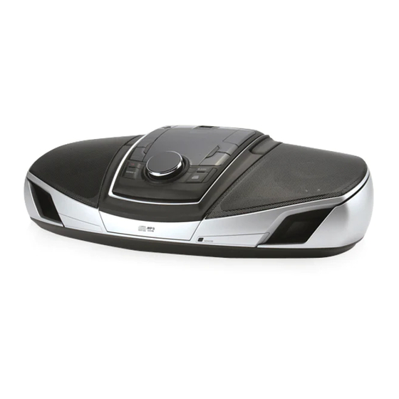
- Page 1 Internal Use Only Website http://biz.lgservice.com Stylish Powerful Portable Boom Box SERVICE MANUAL CAUTION BEFORE SERVICING THE UNIT, READ THE “SAFETY PRECAUTIONS” IN THIS MANUAL. MODEL : SB74 P/NO : AFN73250927 SEPTEMBER, 2009...
-
Page 2: Table Of Contents
• CABINET AND MAIN FRAME SECTION (SB74) ....... . . -
Page 3: Servicing Precautions
SECTION 1. GENERAL SERVICING PRECAUTIONS NOTES REGARDING HANDLING OF THE PICK-UP 1. Notes for transport and storage 1) The pick-up should always be left in its conductive bag until immediately prior to use. 2) The pick-up should never be subjected to external pressure or impact. Storage in conductive bag Drop impact 2. - Page 4 NOTES REGARDING COMPACT DISC PLAYER REPAIRS 1. Preparations 1) Compact disc players incorporate a great many ICs as well as the pick-up (laser diode). These compo- nents are sensitive to, and easily affected by, static electricity. If such static electricity is high voltage, components can be damaged, and for that reason components should be handled with care.
-
Page 5: Safety Precautions
SAFETY PRECAUTIONS Electrostatically Sensitive Devices (ESD) Some semiconductor (solid state) devices can be damaged easily by static electricity. Such components commonly are called Electrostatically Sensitive Devices (ESD). Examples of typical ESD devices are integrated circuits and some field-effect transistors and semiconductor chip components. The following techniques should be used to help reduce the incidence of component damage caused by static electricity. - Page 6 PROGRAM UPGRADE PROCESS Important Notice : When ugrade the software running, Do not shut down the power, it may damage the unit 1. Copy the software file into the USB flash, As the file name is [SB74_VXX.mcs] 2. Insert the USB flash into the USB host 3.
-
Page 7: Specifications
SPECIFICATIONS GENERAL Power supply Refer to main label. Power consumption Refer to main label. Net Weight 3.3 kg External dimensions (W x H x D) 524 x 155 x 288 mm Laser Semiconductor laser, wave length 780nm Frequency response (Audio) 100Hz to 18KHz Single to noise ratio More than 55dB... -
Page 8: Cabinet And Main Frame Section (Sb74)
SECTION 2. EXPLODED VIEWS NOTES) THE EXCLAMATION POINT WITHIN AN EQUILATERAL TRIANGLE IS INTENDED TO ALERT THE SERVICE PERSONNEL TO THE PRESENCE OF IMPORTANT SAFETY INFORMATION IN SERVICE • CABINET AND MAIN FRAME SECTION (SB74) LITERATURE. 274L 275L 252A 275R 274R... -
Page 10: Packing Accessory Section
• PACKING ACCESSORY SECTION Remote Control Battery Instruction Ass Packing Packing... -
Page 12: Troubleshooting Guide
SECTION 3. ELECTRICAL PART TROUBLESHOOTING GUIDE 1. SMPS PART Is the F901 nomal? Replace the F901 (Use same type Fuse) Is the BD901 nomal? Replace the BD901 Is the R901 nomal? Replace the R901 Is Vcc(9V~25V) supplied to IC911 pin5? Is the D911 nomal? Check or replace the D911 Is the D952 nomal? - Page 13 3. MUTING CIRCUIT (MUTE) Does “High” appear Check JK601 pin50 Check R202,R203 Check D205,D204 at Q206, Q208 “B”? Check the “Low” of Replace Q206, Q208 Check R635 Q206, Q208 “C” Check the IC603 pin81 MUTE “HIGH” or “LOW” Replace IC603 4.
- Page 14 5. AUDIO ABNORMAL (FUNCTION MODE) PORTABLE Check the input Check the input Check L800, L802 Check R800, R801 signal of U503 pin7,8 signal CN500 Check the output signal Check C810, C811 of U503 pin19,23 CD / USB Check the output signal of U703 pin55, 57 Check the input signal of U503 pin3, 4 and refer to CD troubleshooting Check the output signal of U503 pin19, 23...
- Page 15 6. U302/3.3V ABNORMAL U302 3.3V output Check Q308 output Check Replace ZD302 normal ? normal? ZD302 normal? Replace R308 Check R308 Check D301 Replace D301 Check R328 Replace R328 Check or replace Check Q302 output Check ECO-POWER R305,R303,Q301 is “HIHGT” Replace F301 Check F301 Refer to SMPS...
- Page 16 8. IC600 ABNORMAL Refer to power supply no 3.3V, Check both end voltage Q600 (3.3V) check or replace Q600 Check IC606 pin1 is “H”, Check Q601 is “H” Check or replace Q601 Check IC604 pin13 is 3.3V Check or replace L600 Check IC600 pin1, 6 X601 operation Check or replace X601 9.
- Page 17 11. U503 ABNORMAL Check the power supply to U503 pin24 Refer to power circuit troubleshooting Check the SCL/SDA data of U503 pin25, 26 Check JK601 pin47, 48 Vol_CLK/Vol_Data Check the control function Check or replace U503 12. U501 ABNORMAL LCD display check Check the power Refer to power supply supply to U501 pin7...
- Page 18 14. CD PART Turn on CD Check JK500/JK501 Check Open/Close Check R730,R731 pin34(Open 3.3V Close 0V) Check CN703 Check “READING” display Check Reading OK Check CN703 Check pickup movement Check U704 BA5927FM Check U703 Check U703 pin55, 57 Playing, check audio output 15.
- Page 19 16. USB PART Turn on the USB Check “CHECKING” Check connector locking Check Power supply circuit or “USB” display CN401, CN705 Q316 USB+5V Check CN401 Check CN705 Check MICOM IC603 Check reading pin2_5V pin3, 4 (D+, D-) pin116, 117 (D+, D-) Playing, Check U703 Check U503 pin3, 4...
-
Page 20: Waveforms Of Major Check Point
WAVEFORMS OF MAJOR CHECK POINT 1. SPINDLE DRIVE AND MOTOR WAVEFORM U704 pin19 U704 pin20 U704 pin22 U704 pin21 2. WHEN CD PLAYING FE/EE/TE/SP+ WAVEFORM U703 pin62 U703 pin61 U703 pin60 U704 pin21... - Page 21 3. WHEN CD SEARCHING EE/TE/FE WAVEFORM U703 pin61 U703 pin62 U703 pin60 4. WHEN CD PLAYING FD/TD WAVEFORM U703 pin14 U703 pin13 3-10...
- Page 22 5. CD STOP ACTION SLE+/SP+/T+/F+ WAVEFORM U704 pin21 U704 pin20 SLE+ U704 pin4 U704 pin2 6. CD READING CD-MCK/DIN/RW/BUSY WAVEFORM U703 pin41 U703 pin19 U703 pin20 U703 pin21 BUSY 3-11...
- Page 23 7. WHEN CD PLAYING RF WAVEFORM U703 pin63 8. CD READING DAC-LRCK/BCK/MCK/DATA WAVEFORM U703 pin39 LRCK U703 pin40 U703 pin41 DATA U703 pin38 3-12...
- Page 24 9. WHEN USB OPERATING D-/+5V/D+ WAVEFORM CN705 pin4 CN705 pin2 CN705 pin3 10. RADIO OPERATING TU-DA/CLK/RST WAVEFORM U101 pin2 SDIO U101 pin8 U101 pin1 3-13...
-
Page 25: Wiring Diagram
WIRING DIAGRAM 3-14... -
Page 26: Block Diagrams
BLOCK DIAGRAM 3-15... - Page 27 3-16...
-
Page 28: Circuit Diagrams
BE MODIFIED OR ALTERED WITH OUT PERMISSION WAY, IMPLEMENTATION OF THE LATEST SAFETY during Play mode. FROM THE LG CORPORATION. ALL COMPONENTS AND PERFORMANCE IMPROVEMENT CHANGES SHOULD BE REPLACED ONLY WITH TYPES INTO THE SET IS NOT DELAYED UNTIL THE NEW IDENTICAL TO THOSE IN THE ORIGINAL CIRCUIT. - Page 29 2. MAIN CIRCUIT DIAGRAM MAIN SB74 WAVEFORM 2009. 07. 10 3-19 3-20...
- Page 30 3. CD CIRCUIT DIAGRAM 7 11 18 25 2 15 SB74 WAVEFORM 2009. 07. 10 3-21 3-22...
- Page 31 4. MCU9800 CIRCUIT DIAGRAM MCU9800 SB74 2009. 07. 10 3-*23 3-24...
- Page 32 5. LCD/USB/PH CIRCUIT DIAGRAM LCD/USB/PH SB74 2009. 07. 10 3-25 3-26...
-
Page 33: Circuit Voltage Chart
CIRCUIT VOLTAGE CHART Pin No. Voltage Pin No. Voltage Pin No. Voltage Pin No. Voltage Pin No. Voltage Pin No. Voltage Pin No. Voltage U501 DGND 0.06 7.75 1.65 1.53 3.08 U301A 3.28 2.29 1.53 DGND 3.34 DGND 2.59 2.93 DGND 11.45 3.34... - Page 34 PRINTED CIRCUIT BOARD DIARGAMS 1-1. MAIN P.C. BOARD DIAGRAM ( TOP VIEW ) 3-29 3-30...
- Page 35 1-2. MAIN P.C. BOARD DIAGRAM ( BOTTOM VIEW ) 3-31 3-32...
- Page 36 2. SMPS P.C. BOARD DIAGRAM NOTE: Warning Parts that are shaded are critical With respect to risk of fire or electrical shock. 3-33 3-34...
- Page 37 3-1. MCU9800 P.C. BOARD DIAGRAM ( TOP VIEW ) 3-35 3-36...
- Page 38 3-2. MCU9800 P.C. BOARD DIAGRAM ( BOTTOM VIEW ) 3-37 3-38...
- Page 39 4. FRONT P.C. BOARD DIAGRAM 5. CD JACK P.C. BOARD DIAGRAM 3-39 3-40...