Table of Contents
Quick Links
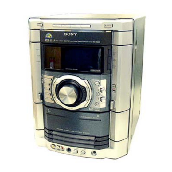
HCD-GN90D/GN100D
SERVICE MANUAL
Ver 1.0 2004. 07
• HCD-GN90D/GN100D are the Amplifier,
DVD player, tape deck and tuner
section in MHC-GN90D/GN100D.
This system incorporates Dolby* Digital, Dolby Pro Logic
(II) adaptive matrix surround decoder, and the DTS** Digital
Surround System.
* Manufactured under license from Dolby Laboratories.
"Dolby", "Pro Logic", and the double-D symbol are
trademarks of Dolby Laboratories.
** Manufactured under license from Digital Theater
Systems, Inc, "DTS" and " DTS Digital Surround" are
registered trademarks of Digital Theater Systems. Inc.
Amplifier section
MHC-GN100D
The following are measured at AC 120, 127, 220, 240V 50/60 Hz
DIN power output (rated)
Front speaker:
180 + 180 watts (6 ohms at 1 kHz, DIN)
Center speaker:
60 watts (8 ohms at 1 kHz, DIN)
Surround speaker:
60 + 60 watts (8 ohms at 1 kHz, DIN)
Continuous RMS power output (reference)
Front speaker:
235 + 235 watts
(6 ohms at 1 kHz, 10% THD)
Center speaker:
80 watts (8 ohms at 1 kHz, 10% THD)
Surround speaker:
80 + 80 watts
(8 ohms at 1 kHz, 10% THD)
MHC-GN90D
The following are measured at AC 120, 127, 220, 240V 50/60 Hz
DIN power output (rated)
Front speaker:
125 + 125 watts (6 ohms at 1 kHz, DIN)
Center speaker:
30 watts (8 ohms at 1 kHz, DIN)
Surround speaker:
30 + 30 watts (8 ohms at 1 kHz, DIN)
Continuous RMS power output (reference)
Front speaker:
170 + 170 watts
(6 ohms at 1 kHz, 10% THD)
Center speaker:
50 watts (8 ohms at 1 kHz, 10% THD)
Surround speaker:
50 + 50 watts
(8 ohms at 1 kHz, 10% THD)
Sony Corporation
9-877-976-01
Home Audio Company
2004G02-1
Published by Sony Engineering Corporation
© 2004.07
Model Name Using Similar Mechanism
DVD
DVD Mechanism Type
Section
Base Unit Name
Optical Pick-up Name
TAPE
Model Name Using Similar Mechanism
Section
SPECIFICATIONS
Inputs
GAME INPUT (VIDEO):
(phono jack)
GAME INPUT (AUDIO):
(phono jacks)
VIDEO/SAT (AUDIO) IN:
(phono jacks)
MIC:
(phone jack)
Outputs
AUDIO OUT:
(phono jacks)
VIDEO OUT:
(phono jack)
COMPONENT VIDEO
OUT:
MiNi Hi-Fi COMPONENT SYSTEM
E Model
HCD-GN90D/GN100D
Australian Model
HCD-GN100D
NEW
CDM74D2-DVBU62
DVBU62
DBU-3
NEW
1 Vp-p, 75 ohms
Voltage 250 mV,
impedance 47 kilohms
voltage 450 mV/250 mV,
impedance 47 kilohms
sensitivity 1 mV,
impedance 10 kilohms
Voltage 250 mV
impedance 1 kilohms
max. output level 1 Vp-p,
unbalanced, Sync.
negative load impedance
75 ohms
Y: 1 Vp-p, 75 ohms
P
/C
: 0.7 Vp-p, 75 ohms
B
B
P
/C
: 0.7 Vp-p, 75 ohms
R
R
– Continued on next page –
Table of Contents

Related Manuals for Sony HCD-GN90D


Summary of Contents for Sony HCD-GN90D
- Page 1 E Model HCD-GN90D/GN100D Australian Model Ver 1.0 2004. 07 HCD-GN100D • HCD-GN90D/GN100D are the Amplifier, DVD player, tape deck and tuner section in MHC-GN90D/GN100D. This system incorporates Dolby* Digital, Dolby Pro Logic Model Name Using Similar Mechanism (II) adaptive matrix surround decoder, and the DTS** Digital Surround System.
- Page 2 LIST ARE CRITICAL TO SAFE OPERATION. REPLACE THESE Other models: 120 V, 220 V or COMPONENTS WITH SONY PARTS WHOSE PART NUMBERS 230 – 240 V AC, 50/60 Hz APPEAR AS SHOWN IN THIS MANUAL OR IN SUPPLEMENTS Adjustable with voltage selector PUBLISHED BY SONY.
-
Page 3: Table Of Contents
HCD-GN90D/GN100D TABLE OF CONTENTS 7-7. Printed Wiring Board – RF Board – ....... 38 SERVICING NOTES ..........4 7-8. Schematic Diagram – RF Board – ........39 7-9. Printed Wiring Board – DVD Mechanism Board – ..40 GENERAL 7-10. Schematic Diagram – DVD Mechanism Board – ..41 Location of Controls ............ -
Page 4: Servicing Notes
HCD-GN90D/GN100D SECTION 1 SERVICING NOTES • MODEL IDENTIFICATION NOTES ON HANDLING THE OPTICAL PICK-UP BLOCK – Back Panel – OR BASE UNIT PART No. The laser diode in the optical pick-up block may suffer electrostatic break-down because of the potential difference generated by the charged electrostatic load, etc. -
Page 5: General
HCD-GN90D/GN100D SECTION 2 GENERAL This section is extracted from instruction manual. LOCATING THE CONTROLS List of button locations and reference pages U nit ALPHABE TICAL OR DER SYMBOLS Power illuminator 2 ?/1 (power) 1 A – D REC PAUSE/START qg... - Page 6 HCD-GN90D/GN100D This section is extracted from instruction manual. Re mot e c ont rol ALPHABE TICAL OR DER SYMBOLS ?/1 (power) 1 A – E F – Z x (stop) 6 ALBUM + 7 FM MODE 5 X (pause) 6 ALBUM –...
-
Page 7: Disassembly
HCD-GN90D/GN100D SECTION 3 DISASSEMBLY • This set can be disassembled in the order shown below. 3-1. DISASSEMBLY FLOW 3-2.CASE (Page 8) 3-3.LOADING PANEL ASSY (Page 8) 3-4.FRONT PANEL ASSY (Page 9) 3-6.TAPE MECHANISM DECK, 3-5.DVD MECHANISM DECK 3-7.CD SW BOARD,... -
Page 8: Case
HCD-GN90D/GN100D Note: Follow the disassembly procedure in the numerical order given. 3-2. CASE 3 five screws (+BVTT3 x 6) 7 case 2 screw (case 3 TP2) (M3 x 12) 1 two screws (case 3 TP2) (M3 x 8) 4 two screws... -
Page 9: Front Panel Assy
HCD-GN90D/GN100D 3-4. FRONT PANEL ASSY 1 two wires (flat type) 3 screw (BVTP3 x 10) 9 front panel assy 8 from CN802 on GAME board MAIN board CN508 CN509 4 screw (BVTP3 x 10) 5 from deck B head 6 from CN801 on GAME board... -
Page 10: Tape Mechanism Deck, Game Board
HCD-GN90D/GN100D 3-6. TAPE MECHANISM DECK, GAME BOARD 2 tape mechanism deck 1 five screws (+BVTP2.6 x 8) 3 three screws (+BVTP2.6 x 8) 4 bracket (MIC) 6 GAME board 5 knob (MIC) 3-7. CD SW BOARD, PANEL BOARD 1 five screws (+BVTP2.6 x 8) -
Page 11: Switch Board
HCD-GN90D/GN100D 3-8. SWITCH BOARD 2 two screws (+BVTP2.6 x 8) 3 SWITCH board 1 two knobs (AMS) 3-9. TUNER PACK 2 two screws 3 tuner pack (+BVTT3 x 6) 1 wire (flat type) (11 core) -
Page 12: Bracket Top, Bracket Sub
HCD-GN90D/GN100D 3-10. BRACKET TOP, BRACKET SUB 4 bracket, top 2 two screws (BVTP3 x 10) 1 four screws (BVTT3 x 6 (S)) 6 connector (CN1200) 5 wire (flat type) (7 core) 8 two screws (CN517) (BVTP3 x 6) 7 wire (flat type) -
Page 13: Dmb07 Board, Video Board
HCD-GN90D/GN100D 3-12. DMB07 BOARD, VIDEO BOARD bracket, top (CN1202) 8 VIDEO board 7 three screws (BVTP3 x 10) (CN105) 3 wire (flat type) (17 core) (CN101) 6 DMB07 board (CN501) 2 wire (flat type) (7 core) 1 wire (flat type) (29 core) -
Page 14: Main Board, Power Board Assy
HCD-GN90D/GN100D 3-14. MAIN BOARD, POWER BOARD ASSY 4 two screws (+BVTT3 x 6 (S)) 2 connector 4p (CN703) 1 connector 6p (CN604) 5 screw (+BVTT3 x 6 (S)) 3 two screws (+BVTT3 x 6 (S)) 7 POWER board assy 6 screw... -
Page 15: Power Transformer (T601)
HCD-GN90D/GN100D 3-16. POWER TRANSFORMER (T601) 3 six screws 4 power transformer (T601) 1 connector 6p (CN604) 2 connector 4p (CN703) 3-17. DRIVER BOARD, SW BOARD 1 two screws (+BTTP (M2.6)) 3 connector 4p (CN703) 4 DRIVER board 5 screw (+BTTP (M2.6)) -
Page 16: Rf Board, Optical Pick-Up (Dbu-3)
HCD-GN90D/GN100D 3-18. RF BOARD, OPTICAL PICK-UP (DBU-3) 8 Step screw (M) 9 Step screw (M) qs Insulator qa Insulator (RB) qf Optical pick-up (DBU-3) 0 Step screw (M) qd Insulator (RB) 6 Floating screw (PTPWH M2.6) qg Holder (DBU) assy... -
Page 17: Motor (Tb) Board
HCD-GN90D/GN100D 3-20. MOTOR (TB) BOARD 2 stopper 1 stopper 7 t able motor assy (M741) 3 wire (flat type) 5 core (CN742) 8 MOTOR (TB) board 6 Remove the two solderings of motor. 5 two screws (+BTTP (M2.6)) 3-21. MOTOR (LD) BOARD 2 two screws (+BTTP (M2.6)) -
Page 18: Test Mode
HCD-GN90D/GN100D SECTION 4 TEST MODE [GC TEST MODE] * Check of Amplifier 1. Press [EQ EDIT] button repeatedly until a message “GEQ MAX” • This mode is used to check the fluorescent indicator tube, LED, appears on the fluorescent indicator tube. GEQ increases to its model, destination, software version, volume, key, jog, encoder maximum. - Page 19 HCD-GN90D/GN100D [VACS ON/OFF] [DVD POWER MANAGE] • This mode is used to switch ON and OFF the VACS (Variable • This mode let you switch on or off power supply to the ZIVA Attenuation Control System). during TUNER function. Procedure: •...
- Page 20 HCD-GN90D/GN100D [DVD PROGRESSIVE] 0-0 Quit Quit the Syscon Diagnosis and return to the Test Mode Menu. • This mode let you change the video signal format from PRO- GRESSIVE format to INTERLACE format if you accidentally 0-1 All (All items continuous check) change the COMPONENT OUT settings in DVD SETUP This menu checks all diagnostic items continuously.
- Page 21 HCD-GN90D/GN100D 0-2-3. ROM Check Sum Note: During adjustment of each disc, the measurement for disc type judg- ment is made. As automatic adjustment does not judge the disc Check sum is calculated. (4 digits hexadecimal number) type unlike conventional models, take care not to insert wrong type discs.
- Page 22 HCD-GN90D/GN100D 19. Auto focus offset adjust 500 track jump reverse 20. Auto focus gain adjust Layer Jump Check 21. Auto focus offset adjust Layer jump (L0 t L1) 22. EQ boost adjust Layer jump (L1 t L0) 23. Auto LFO Adjust 47.
- Page 23 HCD-GN90D/GN100D [4] : SACD Hybrid disc (SACD layer, 8 cm) 2-1-1. Disc Type Auto Check [5] : SACD Hybrid disc (CD layer, normal speed, 8 cm) Press the 1 button on the remote commander to display the [6] : SACD Hybrid disc (CD layer, double speed, 8 cm) Disc Type Auto Check screen.
- Page 24 HCD-GN90D/GN100D [1] 1Tj FWD [1] Focus Offset : Adjusts focus offset. : 1 track jumps forward. [2] 1Tj REV [2] Focus Gain : Adjusts focus gain. : 1 track jump reverse. [3] 500Tj FWD : 500 tracks jump (fine search) forward.
- Page 25 HCD-GN90D/GN100D 2-8. Error Rate Display During aging, the disc number, operating status and repeat cycle are displayed. Aging can be aborted at any time by pressing Error Rate Display the [RETURN] button. After the operation is stopped, press the CR Address [RETURN] button to return to the Aging Test MENU.
- Page 26 HCD-GN90D/GN100D 50 : CLV (spindle) servo does not operate. Version Information 51 : Spindle does not stop. On the Test Mode Menu screen, selecting [6] displays the ROM 60 : Made a request to seek nonexistent address. version and region code. The parenthesized hexadecimal number 61 : Seek error of retry more than regulated times.
-
Page 27: Mechanical Adjustments
HCD-GN90D/GN100D SECTION 5 SECTION 6 MECHANICAL ADJUSTMENTS ELECTRICAL ADJUSTMENTS Precaution DECK SECTION 0 dB=0.775 V 1. Clean the following parts with a denatured alcohol-moistened swab: 1. Demagnetize the record/playback head with a head record/playback heads pinch rollers demagnetizer. erase head rubber belts 2. -
Page 28: Video Section
HCD-GN90D/GN100D 2. Turn the adjustment screw and check output peaks. If the peaks VIDEO SECTION do not match for L-CH and R-CH, turn the adjustment screw so that outputs match within 1dB of peak. RE-ADJUSTMENT OF THE SERVO CIRUIT The re-adjustment of the servo circuit is necessary when the part which relates to the servo circuit is replaced. - Page 29 HCD-GN90D/GN100D RFMON Level Check Perform a RFMON level check before exchanging optical pick-up. Connection: oscilloscope JL005(RFMON) –RF board (side B) – – JL005 (RFMON) RFMON signal waveform VOLT/DIV: 200 mV TIME/DIV: 500 ns RFMON level • Standard value RFMON level...
-
Page 30: Diagrams
HCD-GN90D/GN100D SECTION 7 DIAGRAMS For schematic diagrams. Note on Printed Wiring Boards: Note: • X : parts extracted from the component side. • All capacitors are in µF unless otherwise noted. (p: pF) • : Pattern from the side which enables seeing. - Page 31 VOL/DIV : 1 V AC TIME/DIV : 0.2 µ sec 15.3 MHz VOL/DIV : 0.5 V AC VOL/DIV : 0.5 V AC VOL/DIV : 1 V AC TIME/DIV : 20 µ sec TIME/DIV : 0.1 µ sec TIME/DIV : 20 nsec HCD-GN90D/GN100D...
-
Page 32: Block Diagram - Dvd Section (1/2)
49 27 50 9 72 71 30 74 75 14-21 89-96 22 23 81 80 D0-D7 A0-A7 IC903 EEPROM 40 XTAL X901 SDA_EEP 5 SDA • Signal path 20MHz 41 EXTAL SCL_EEP : DVD WP_EEP c : DIGITAL OUT HCD-GN90D/GN100D... -
Page 33: Block Diagram - Dvd Section (2/2)
DRIVE (LOADING) MECHANISM CONTROLLER OUT2 IC401 (1/5) TM-F MOTOR M741 SYSTEM OUT1 DRIVE (TABLE) TM-R CONTROL IC712 MOTOR DRIVER RE701 ROTARY ENCODER • Signal path : DVD c : DIGITAl OUT g : VIDEO k : GAME IN (VIDEO) HCD-GN90D/GN100D... -
Page 34: Block Diagram - Tuner/Tape Section
• R-ch is omitted due to same as L-ch. • Signal path AM ANT ST-DOUT/MC-DIN ST-DIN : TAPE PLAY (DECK A) ST-DIN/MC-DOUT ST-DOUT : TAPE PLAY (DECK B) AM ANT ST-CLK ST-CLK : RECORD ST-CE ST-CE ANTENNA : TUNER (FM/AM) HCD-GN90D/GN100D... -
Page 35: Block Diagram - Main Section
(Page 36) SYSTEM CONTROL IC401 (3/5) • R-ch is omitted due to same as L-ch. • Signal path : TUNER (FM/AM) : DVD : TAPE PLAY : RECORD : MIC INPUT : MD/VIDEO (AUDIO) IN : GAME IN (AUDIO) HCD-GN90D/GN100D... -
Page 36: Block Diagram - Display/Power Section
15 X-IN EVER +4V AC IN REGULATOR X402 16MHz LEVEL 13 X-OUT RESET DETECT RESET SWITCH IC301 Q301 D504 10 XC-IN X501 AC-CUT 32.768kHz D503 • Abbreviation 11 XC-OUT AVCC : Mexican model D501 AUS : Australian model MCU VCC HCD-GN90D/GN100D... -
Page 37: Block Diagram - Amp Section
USE 8Ω Q740 GN100D IC700 Q763 J701 (2/2) POWER AMP RY761 Q765 RTS1 TH630 DISPLAY/POWER CLK1 SECTION (Page 36) DELAY Q402 SYSTEM CONTROL IC401 (4/5) • R-ch is omitted due to same as L-ch • Signal path. : TUNER (FM/AM) HCD-GN90D/GN100D... -
Page 38: Printed Wiring Board - Rf Board
• See page 68 for Circuit Boards Location. (SIDE A) (SIDE B) RF BOARD RF BOARD OPTICAL PICK-UP BLOCK (DBU-3) DMB07 BOARD (Page 42) OPTICAL PICK-UP BLOCK (DBU-3) 1-684-822- 1-684-822- (12) (12) • Semiconductor Location Ref. No. Location D001 D002 IC001 IC003 Q001 Q002 HCD-GN90D/GN100D... -
Page 39: Schematic Diagram - Rf Board
HCD-HCDGN90D/GN100D 7-8. SCHEMATIC DIAGRAM – RF BOARD – • See page 71 for IC Block Diagram. • See page 31 for Waveforms. HCD-GN90D/GN100D... -
Page 40: Printed Wiring Board - Dvd Mechanism Board
HCD-HCDGN90D/GN100D 7-9. PRINTED WIRING BOARD – DVD MECHANISM BOARD – • See page 68 for Circuit Boards Location. MAIN BOARD CN301 (Page 52) S751 (LEVER SW) CN751 • Semiconductor Location Ref. No. Location D701 D711 IC701 IC712 IC731 Q731 HCD-GN90D/GN100D... -
Page 41: Schematic Diagram - Dvd Mechanism Board
HCD-HCDGN90D/GN100D 7-10. SCHEMATIC DIAGRAM – DVD MECHANISM BOARD – • See page 70 for IC Block Diagram. HCD-GN90D/GN100D... -
Page 42: Printed Wiring Board - Dmb07 Board (Side A)
• Semiconductor Location Ref. No. Location D202 D901 D1303 D1304 IC207 IC211 IC231 IC232 IC256 IC258 IC259 IC302 IC503 IC509 IC701 IC901 IC902 IC904 IC906 Q201 MAIN BOARD (Page 52) 1-861-848- (12) MAIN BOARD RF BOARD (Page 52) (Page 38) HCD-GN90D/GN100D... -
Page 43: Printed Wiring Board - Dmb07 Board (Side B)
• See page 68 for Circuit Boards Location. (SIDE B) DMB07 BOARD • Semiconductor Location Ref. No. Location D392 D393 D394 D500 IC111 IC203 IC204 IC205 IC233 IC352 IC392 IC501 IC502 IC703 IC706 IC903 IC907 Q202 Q901 1-861-848- (12) HCD-GN90D/GN100D... -
Page 44: Schematic Diagram - Dmb07 Board (1/6)
HCD-HCDGN90D/GN100D 7-13. SCHEMATIC DIAGRAM – DMB07 BOARD (1/6) – • See page 69 for IC Block Diagram. • See page 31 for Waveforms. HCD-GN90D/GN100D... -
Page 45: Schematic Diagram - Dmb07 Board (2/6)
HCD-HCDGN90D/GN100D • See page 80 for IC Pin Function Description. • See page 70 for IC Block Diagram. • See page 31 for Waveforms. 7-14. SCHEMATIC DIAGRAM – DMB07 BOARD (2/6) – HCD-GN90D/GN100D... -
Page 46: Schematic Diagram - Dmb07 Board (3/6)
HCD-HCDGN90D/GN100D 7-15. SCHEMATIC DIAGRAM – DMB07 BOARD (3/6) – • See page 72 for IC Pin Function Description. • See page 70 for IC Block Diagram. • See page 31 for Waveforms. VIDEO _SW HCD-GN90D/GN100D... -
Page 47: Schematic Diagram - Dmb07 Board (4/6)
HCD-HCDGN90D/GN100D 7-16. SCHEMATIC DIAGRAM – DMB07 BOARD (4/6) – • See page 76 for IC Pin Function Description. • See page 31 for Waveforms. HCD-GN90D/GN100D... -
Page 48: Schematic Diagram - Dmb07 Board (5/6)
HCD-HCDGN90D/GN100D 7-17 SCHEMATIC DIAGRAM – DMB07 BOARD (5/6) – HCD-GN90D/GN100D... -
Page 49: Schematic Diagram - Dmb07 Board (6/6)
HCD-HCDGN90D/GN100D 7-18. SCHEMATIC DIAGRAM – DMB07 BOARD (6/6) – • See page 69 for IC Block Diagram. HCD-GN90D/GN100D... -
Page 50: Printed Wiring Board - Video Board
7-19. PRINTED WIRING BOARD – VIDEO BOARD – • See page 68 for Circuit Boards Location. DMB07 BOARD (Page 42) VIDEO BOARD MAIN BOARD (Page 52) GAME BOARD (Page 60) (11) 1-862-130 VIDEO OUT S VIDEO OUT PB/CB PR/CR COMPONENT VIDEO OUT HCD-GN90D/GN100D... -
Page 51: Schematic Diagram - Video Board
HCD-HCDGN90D/GN100D 7-20. SCHEMATIC DIAGRAM – VIDEO BOARD – • See page 70 for IC Block Diagram. • See page 31 for Waveforms. HCD-GN90D/GN100D... -
Page 52: Printed Wiring Boards - Main Board
Q519 Q111 Q520 J-10 Q112 Q521 I-12 Q113 Q523 I-12 Q114 Q524 I-12 Q115 Q526 Q116 Q527 Q117 Q568 E-12 Q118 Q570 J-10 1-861-399- (CHASSIS) Q119 Q813 Q120 Q863 Q121 PA BOARD PA BOARD Q122 (Page 62) (Page 62) HCD-GN90D/GN100D... -
Page 53: Schematic Diagram - Main Board (1/4)
HCD-HCDGN90D/GN100D 7-22. SCHEMATIC DIAGRAM – MAIN BOARD (1/4) – • See page 73 for IC Pin Function Description. • See page 31 for Waveforms. HCD-GN90D/GN100D... -
Page 54: Schematic Diagram - Main Board (2/4)
HCD-HCDGN90D/GN100D 7-23. SCHEMATIC DIAGRAM – MAIN BOARD (2/4) – HCD-GN90D/GN100D... -
Page 55: Schematic Diagram - Main Board (3/4)
HCD-HCDGN90D/GN100D 7-24. SCHEMATIC DIAGRAM – MAIN BOARD (3/4) – HCD-GN90D/GN100D... -
Page 56: Schematic Diagram - Main Board (4/4)
HCD-HCDGN90D/GN100D 7-25. SCHEMATIC DIAGRAM – MAIN BOARD (4/4) – HCD-GN90D/GN100D... -
Page 57: Printed Wiring Board - Panel Board
D918 D919 D920 D921 MAIN D922 BOARD D923 (Page 52) D924 IC901 IC902 IC903 (VOL 7) Q901 SWITCH Q904 BOARD (Page 60) Q905 Q906 Q907 Q908 Q909 Q910 Q911 Q912 Q913 Q914 Q915 Q916 1-861-403- (11) BOARD (Page 60) HCD-GN90D/GN100D... -
Page 58: Schematic Diagram - Panel Board (1/2)
HCD-HCDGN90D/GN100D 7-27. SCHEMATIC DIAGRAM – PANEL BOARD (1/2) – • See page 72 for IC Pin Function Description. • See page 31 for Waveforms. HCD-GN90D/GN100D... -
Page 59: Schematic Diagram - Panel Board (2/2)
HCD-HCDGN90D/GN100D 7-28. SCHEMATIC DIAGRAM – PANEL BOARD (2/2) – HCD-GN90D/GN100D... -
Page 60: Printed Wiring Boards - Game, Cd Sw Board
(Page 57) PANEL BOARD 1-861-407- (11) (Page 57) 1-861-406- (11) GAME BOARD • Semiconductor Location Ref. No. Location D801 1-861-404- (11) D802 D803 VIDEO MAIN D806 BOARD BOARD D807 (Page 50) (Page 52) D925 A-10 IC850 IC851 Q917 A-10 HCD-GN90D/GN100D... -
Page 61: Schematic Diagram - Game, Cd Sw Board
HCD-HCDGN90D/GN100D 7-30. SCHEMATIC DIAGRAM – GAME, CD SW BOARD – • See page 70 for IC Block Diagram. HCD-GN90D/GN100D... -
Page 62: Printed Wiring Board - Pa Board
D612 D620 D624 1-861-400- D646 (12) D654 D-10 D655 D-10 D656 D658 D660 D661 D664 D670 D699 IC600 Q604 Q606 Q610 Q618 Q628 Q629 Q630 Q634 Q640 Q641 Q644 Q647 Q648 Q664 Q666 Q668 Q682 POWER TRANSFORMER (Page 66) HCD-GN90D/GN100D... -
Page 63: Schematic Diagram - Pa Board
HCD-HCDGN90D/GN100D 7-32. SCHEMATIC DIAGRAM – PA BOARD – HCD-GN90D/GN100D... -
Page 64: Printed Wiring Board - Surround Board
• Semiconductor Location Ref. No. Location D701 D702 D730 D760 D761 D762 D763 D764 D770 D780 IC700 IC705 Q700 Q701 Q730 Q740 Q750 PRIMARY 1-861-401- (12) Q762 BOARD Q763 (Page 66) Q764 Q765 Q770 POWER Q780 TRANSFORMER (Page 66) HCD-GN90D/GN100D... -
Page 65: Schematic Diagram - Surround Board
HCD-HCDGN90D/GN100D 7-34. SCHEMATIC DIAGRAM – SURROUND BOARD – HCD-GN90D/GN100D... -
Page 66: Printed Wiring Boards - Primary Board
HCD-HCDGN90D/GN100D 7-35. PRINTED WIRING BOARD – PRIMARY BOARD – • See page 68 for Circuit Boards Location. PRIMARY BOARD BOARD (Page 62) VOLTAGE SELECT SURROUND BOARD (Page 64) (12) 1-816-402- SURROUND BOARD (Page 64) HCD-GN90D/GN100D... -
Page 67: Schematic Diagram - Primary Board
HCD-GN90D/GN100D 7-36. SCHEMATIC DIAGRAM – PRIMARY BOARD –... -
Page 68: Circuit Board Location
HCD-GN90D/GN100D 7-37. CIRCUIT BOARD LOCATION PRIMARY board VIDEO board DMB07 board TUNER PACK CD SW board SURROUND board SWITCHING POWER PA board JOG board SENSOR board RF board SW board MOTOR (TB) board MOTOR (LD) board DRIVER board PANEL board... -
Page 69: Ic Block Diagram
HCD-GN90D/GN100D 7-38. IC Block Diagrams IC302 PCM1609KPTR (DMB07 BOARD) 32 31 30 36 35 34 33 VCC3 FUNCTION AGND3 CONTROL VCC4 INTERFACE AGND4 SYSTEM SCKI CLOCK SCKO MANAGER VOUT8 AGND6 VCC5 LRCK AGND5 TEST 4X/8X ENHANCED VOUT7 OVER SAMPLING MULTI-... - Page 70 HCD-GN90D/GN100D IC906 SM8707GV-G-E2 (DMB07 BOARD) IC1200 NJM2244M-TE2 (VIDEO BOARD) VDD1 VIN1 VSS1 PHASE PHASE Div.1 DETECTOR1 PUMP1 75 Ω VOUT DRIVER LOOP Div.1 VDD2 VIN2 BIAS VDD3 VSS2 CONTROL LOGIC VIN3 VSS3 X'tal IC706 MSM51V18165F-60TSKR1 (DMB07 BOARD) 40 – 36...
- Page 71 HCD-GN90D/GN100D IC001 SP3723CAF0PM (RF BOARD) 64 63 62 61 60 59 55 54 53 52 FAST ATTACK INPUT OUTPUT HOLD FULL WAVE AGC CHARGE INHIBIT RECTIFER PUMP PROGRAMMABLE FROM S-PORT EQUALIZER INPUT DVDRFP BIAS FILTER DVDRFN DIFFERENTIATOR INPUT INPUT IMPEDANCE...
- Page 72 HCD-GN90D/GN100D • IC Pin Function Descriptions • IC901 MB90M407PF-G-140-BNDE1 DISPLAY CONTROL (PANEL Board) Pin No. Pin Name Description 1 to 5 G5 to G1 FLD grid output 6 to 10 P1 to P5 FLD segment output VSS-IO — Ground 12 to 22...
- Page 73 HCD-GN90D/GN100D • IC401 M3062CMCN-A33FPUO SYSTEM CONTOL (MAIN Board) Pin No. Pin Name Description XRST DVD reset signal output (Not used) CD-DATA DVD data output (Not used) XLAT DVD latch signal output (Not used) SIRCS SIRCS input MP3 DATA OUT Serial data output (Not used)
- Page 74 HCD-GN90D/GN100D Pin No. Pin Name Description TM-F Table motor control signal output TM-R Table motor control signal output Loading motor control signal output Loading motor control signal output A-PLAY TCM-A play switch input A-TRIG TCM-A trigger output A-HALF A deck half detection signal input...
- Page 75 HCD-GN90D/GN100D Pin No. Pin Name Description FUSELESS SW Over-voltage protection detection input termnal VREF Reference voltage input AVCC — Power supply (+3.3V) XTCN/MIC DET MIC detect signal output...
- Page 76 HCD-GN90D/GN100D • IC207 ZIVA5X-C2F (DVD SYSTEM PROCESSOR)(DMB07 BOARD) Pin No. Pin Name Description VDDP — Power supply (+3.3V) Address bus to MBM29L32BM 3 to 11 HAD15 to HAD7 Address/ Data bus to MBM29L32BM VDDP — Power supply (+3.3V) GNDP —...
- Page 77 HCD-GN90D/GN100D Pin No. Pin Name Description GND25 — Ground MDQM3 Byte read /write mask signal 3 output to HY57V283220T6 VDD25 — Power supply (+3.3V) 99 to 102 MD28 to MD31 Data bus to HY57V283220T6 GND25 — Ground VDD25 — Power supply (+3.3V)
- Page 78 HCD-GN90D/GN100D Pin No. Pin Name Description LRCK LRCK signal output to PCM1609KPTR BCK signal output to PCM1609KPTR DATA0(DM) Audio data(Down Mix signal) output to PCM1609KPTR DATA1(FLR) Audio data(Front L/R signal) output to PCM1609KPTR VDDP — Power supply (+3.3V) GNDP —...
- Page 79 HCD-GN90D/GN100D Pin No. Pin Name Description — Ground — Power supply (+1.8V) Address bus to MBM29L32BM Address bus to MBM29L32BM GNDP — Ground...
- Page 80 HCD-GN90D/GN100D • IC701 TMC57929PGF-RDP (DVD DECODER)(DMB07 BOARD) Pin No. Pin Name Description 1, 2 D5, D6 Two-way data bus with CXP973064 — Ground Two-way data bus with CXP973064 Address signal input from CXP973064 — Power supply (+3.3V) Address signal input from CXP973064 VDD5V —...
- Page 81 HCD-GN90D/GN100D Pin No. Pin Name Description XPDI Not used (Pull up) VDDS — Power supply (+5V) 59, 60 HA0, HA2 Not used (Pull up) — Ground (open) 62, 63 HCS0, HCS1 Not used (open) — Power supply (+3.3V) DASP Not used (Pull up)
- Page 82 HCD-GN90D/GN100D Pin No. Pin Name Description 128, 129 VCCA3, VCCA2 — Power supply (+3.3V) Signal output from the charge pump for phase comparator PDHVCC Middle point voltage input terminal for RF PLL Signal output from the charge pump for frequency comparator...
- Page 83 HCD-GN90D/GN100D • IC901 CXP973064-245R (MECHANISM CONTROLLER)(DMB07 BOARD) Pin No. Pin Name Description NO_USE Not used (open) SDEN Serial data enable signal output to SP3723BDA0PM DOCTRL/ Digital out on/off control signal output to CXD3068Q ISBTEST XRST_2753 Not used SDA_EEP Data bus with BR24L16F...
- Page 84 HCD-GN90D/GN100D Pin No. Pin Name Description CONTROL_1 Not used (open) GFS_DVD Guard frame sync signal input from TMC57929PGF MUTE_CD Muting on/off control signal output to CXD3068Q MUTE_2D Muting on/off control signal output to FAN8035L SLED Sled motor servo drive PWM signal input from CXD3068Q...
-
Page 85: Exploded Views
A-4753-146-A PRIMARY BOARD, COMPLETE (AUS) X-4956-408-1 LOADING PANEL ASSY (GN100D) 1-500-497-11 FILTER, CLAMP (FERRITE CORE) X-4956-410-1 LOADING PANEL ASSY (GN90D) 1-693-603-31 TUNER (FM/AM) 4-963-404-21 EMBLEM (5-A), SONY 3-363-099-02 SCREW (CASE 3 TP2) 1-468-737-21 POWER, SWITCHING 4-231-828-71 CASE 3-363-099-32 SCREW (CASE 3 TP2) -
Page 86: Front Panel Section
HCD-GN90D/GN100D 8-2. FRONT PANEL SECTION supplied supplied supplied FL901 supplied supplied supplied supplied Ref. No. Part No. Description Remarks Ref. No. Part No. Description Remarks 1-773-109-11 WIRE (FLAT TYPE) (19 CORE) X-4956-409-1 FRONT PANEL ASSY 4-252-592-01 COVER AL-TC 4-224-104-11 DAMPER... -
Page 87: Chassis Section
HCD-GN90D/GN100D 8-3. CHASSIS SECTION supplied supplied F760 F761 supplied supplied supplied supplied F696 F697 F698 supplied F699 supplied supplied supplied supplied supplied supplied The components identified by T601 mark 0 or dotted line with mark 0 are critical for safety. -
Page 88: Dvd Mechanism Deck Section-1 (Cdm74D2-Dvbu62)
HCD-GN90D/GN100D 8-4. DVD MECHANISM DECK SECTION-1 (CDM74D2-DVBU62) M741 CD mechanism deck section-2 Ref. No. Part No. Description Remarks Ref. No. Part No. Description Remarks 4-243-820-01 GEAR (TABLE) 4-218-253-22 SCREW (M2.6), +BTTP 1-776-182-11 WIRE (FLAT TYPE) (5 CORE) 4-243-819-01 GEAR (GENEVA) -
Page 89: Dvd Mechanism Deck Section-2 (Cdm74D2-Dvbu62)
HCD-GN90D/GN100D 8-5. DVD MECHANISM DECK SECTION-2 (CDM74D2-DVBU62) RE701 M751 The components identified by mark 0 or dotted line with mark 0 are critical for safety. Replace only with part number specified. Ref. No. Part No. Description Remarks Ref. No. Part No. -
Page 90: Electrical Parts List
HCD-GN90D/GN100D SECTION 9 CD SW DMB07 ELECTRICAL PARTS LIST NOTE: • Due to standardization, replacements in the • COILS The components identified by mark 0 uH: µH parts list may be different from the parts or dotted line with mark 0 are critical specified in the diagrams or the components •... - Page 91 HCD-GN90D/GN100D DMB07 Ref. No. Part No. Description Remarks Ref. No. Part No. Description Remarks C264 1-164-943-11 CERAMIC CHIP 0.01uF C509 1-164-934-11 CERAMIC CHIP 330PF C265 1-117-370-11 CERAMIC CHIP 10uF C510 1-164-937-11 CERAMIC CHIP 0.001uF C266 1-164-943-11 CERAMIC CHIP 0.01uF C267 1-164-943-11 CERAMIC CHIP 0.01uF...
- Page 92 HCD-GN90D/GN100D DMB07 Ref. No. Part No. Description Remarks Ref. No. Part No. Description Remarks C709 1-125-777-11 CERAMIC CHIP 0.1uF C906 1-164-943-11 CERAMIC CHIP 0.01uF C711 1-119-923-11 CERAMIC CHIP 0.047uF C907 1-164-943-11 CERAMIC CHIP 0.01uF C712 1-164-874-11 CERAMIC CHIP 100PF C713 1-125-777-11 CERAMIC CHIP 0.1uF...
- Page 93 HCD-GN90D/GN100D DMB07 Ref. No. Part No. Description Remarks Ref. No. Ref. No. Part No. Part No. Description Description Remarks Remarks FL901 1-234-177-21 FILTER, CHIP EMI 1-216-801-11 METAL CHIP 1/10W FL903 1-234-177-21 FILTER, CHIP EMI 1-216-801-11 METAL CHIP 1/10W FL908 1-234-177-21 FILTER, CHIP EMI...
- Page 94 HCD-GN90D/GN100D DMB07 Ref. No. Part No. Description Remarks Ref. No. Part No. Description Remarks R283 1-218-847-11 METAL CHIP 0.5% 1/10W R536 1-216-833-11 METAL CHIP 1/10W R284 1-218-829-11 METAL CHIP 0.5% 1/10W R537 1-216-843-11 METAL CHIP 1/10W R290 1-216-809-11 METAL CHIP...
- Page 95 HCD-GN90D/GN100D DMB07 DRIVER Ref. No. Part No. Description Remarks Ref. No. Part No. Description Remarks R725 1-216-824-11 METAL CHIP 1.8K 1/10W R923 1-216-813-11 METAL CHIP 1/10W R726 1-216-845-11 METAL CHIP 100K 1/10W R925 1-216-809-11 METAL CHIP 1/10W R727 1-216-827-11 METAL CHIP 3.3K...
- Page 96 HCD-GN90D/GN100D DRIVER GAME Ref. No. Part No. Description Remarks Ref. No. Part No. Description Remarks C752 1-164-159-11 CERAMIC 0.1uF C822 1-126-947-11 ELECT 47uF C823 1-162-965-11 CERAMIC CHIP 0.0015uF 10% < CONNECTOR > C824 1-162-969-11 CERAMIC CHIP 0.0068uF 10% CN701 1-785-338-11 PIN, CONNECTOR (LIGHT ANGLE) 12P...
- Page 97 HCD-GN90D/GN100D GAME MAIN Ref. No. Part No. Description Remarks Ref. No. Part No. Description Remarks R802 1-216-825-11 METAL CHIP 2.2K 1/10W < CAPACITOR > R803 1-216-825-11 METAL CHIP 2.2K 1/10W R804 1-216-809-11 METAL CHIP 1/10W C101 1-124-261-00 ELECT 10uF R805...
- Page 98 HCD-GN90D/GN100D MAIN Ref. No. Part No. Description Remarks Ref. No. Part No. Description Remarks C161 1-100-436-91 CERAMIC CHIP 0.033uF C248 1-164-156-11 CERAMIC CHIP 0.1uF C162 1-162-969-11 CERAMIC CHIP 0.0068uF 10% C163 1-126-964-11 ELECT 10uF C249 1-127-715-91 CERAMIC CHIP 0.22uF C164 1-136-170-00 FILM 0.27uF...
- Page 99 HCD-GN90D/GN100D MAIN Ref. No. Part No. Description Remarks Ref. No. Part No. Description Remarks C515 1-164-156-11 CERAMIC CHIP 0.1uF D303 8-719-988-61 DIODE 1SS355TE-17 C517 1-125-827-91 CERAMIC CHIP D501 8-719-988-61 DIODE 1SS355TE-17 C518 1-125-827-91 CERAMIC CHIP D502 6-500-508-01 DIODE RR263M-400FTR C520 1-126-961-11 ELECT 2.2uF...
- Page 100 HCD-GN90D/GN100D MAIN Ref. No. Part No. Description Remarks Ref. No. Part No. Description Remarks JR115 1-216-864-11 SHORT CHIP L105 1-414-189-31 INDUCTOR 100uH JR116 1-216-296-11 SHORT CHIP L501 1-456-468-11 INDUCTOR 100uH JR117 1-216-864-11 SHORT CHIP L502 1-456-467-11 INDUCTOR 100uH JR118 1-216-864-11 SHORT CHIP...
- Page 101 HCD-GN90D/GN100D MAIN Ref. No. Part No. Description Remarks Ref. No. Part No. Description Remarks Q511 8-729-113-69 TRANSISTOR FN1F4M-M32 R142 1-216-833-11 METAL CHIP 1/10W Q513 8-729-802-80 TRANSISTOR 2SC3661 R143 1-216-827-11 METAL CHIP 3.3K 1/10W Q514 8-729-027-23 TRANSISTOR DTA114EKA-T146 Q515 8-729-027-43 TRANSISTOR DTC114EKA-T146...
- Page 102 HCD-GN90D/GN100D MAIN Ref. No. Part No. Description Remarks Ref. No. Part No. Description Remarks R208 1-216-857-11 METAL CHIP 1/10W R301 1-216-813-11 METAL CHIP 1/10W R215 1-216-821-11 METAL CHIP 1/10W R302 1-216-829-11 METAL CHIP 4.7K 1/10W R216 1-216-833-11 METAL CHIP 1/10W...
- Page 103 HCD-GN90D/GN100D MAIN Ref. No. Part No. Description Remarks Ref. No. Part No. Description Remarks R445 1-216-809-11 METAL CHIP 1/10W R516 1-216-835-11 METAL CHIP 1/10W R446 1-216-809-11 METAL CHIP 1/10W R517 1-216-841-11 METAL CHIP 1/10W R447 1-216-809-11 METAL CHIP 1/10W R518...
- Page 104 HCD-GN90D/GN100D MAIN MOTOR (LD) MOTOR (TB) Ref. No. Part No. Description Remarks Ref. No. Part No. Description Remarks < TRANSFORMER > C658 1-100-619-11 ELECT 4700uF (GN90D) T101 1-433-372-11 TRANSFORMER, BIAS OSCILLATION C658 1-112-032-11 ELECT 4700uF < VIBRATOR > (GN100D) C659 1-136-497-81 FILM 0.1uF...
- Page 105 HCD-GN90D/GN100D Ref. No. Part No. Description Remarks Ref. No. Part No. Description Remarks JR602 1-216-296-11 SHORT CHIP R620 1-216-839-11 METAL CHIP 1/10W JR603 1-216-296-11 SHORT CHIP (GN100D) R621 1-216-845-11 METAL CHIP 100K 1/10W < COIL > (GN100D) R621 1-216-847-11 METAL CHIP...
- Page 106 HCD-GN90D/GN100D PANEL Ref. No. Part No. Description Remarks Ref. No. Part No. Description Remarks R670 1-216-839-11 METAL CHIP 1/10W C915 1-162-970-11 CERAMIC CHIP 0.01uF (GN100D) C916 1-164-156-11 CERAMIC CHIP 0.1uF R671 1-216-845-11 METAL CHIP 100K 1/10W C917 1-162-970-11 CERAMIC CHIP 0.01uF...
- Page 107 HCD-GN90D/GN100D PANEL Ref. No. Part No. Description Remarks Ref. No. Part No. Description Remarks C984 1-162-927-11 CERAMIC CHIP 100PF < TRANSISTOR > C985 1-162-927-11 CERAMIC CHIP 100PF C1301 1-164-156-11 CERAMIC CHIP 0.1uF Q901 8-729-027-56 TRANSISTOR DTC143TKA-T146 Q904 8-729-106-60 TRANSISTOR 2SB1115A-YQ <...
- Page 108 HCD-GN90D/GN100D PANEL PRIMARY Ref. No. Part No. Description Remarks Ref. No. Part No. Description Remarks R941 1-216-809-11 METAL CHIP 1/10W R1332 1-216-823-11 METAL CHIP 1.5K 1/10W R942 1-216-809-11 METAL CHIP 1/10W R943 1-216-829-11 METAL CHIP 4.7K 1/10W < SWITCH >...
- Page 109 HCD-GN90D/GN100D PRIMARY Ref. No. Part No. Description Remarks Ref. No. Part No. Description Remarks < COIL > C036 1-125-891-11 CERAMIC CHIP 0.47uF L1001 1-410-666-31 INDUCTOR 18uH C037 1-115-412-11 CERAMIC CHIP 680PF C038 1-164-677-11 CERAMIC CHIP 0.033uF < TRANSISTOR > C039 1-164-677-11 CERAMIC CHIP 0.033uF...
- Page 110 HCD-GN90D/GN100D SENSOR SURROUND Ref. No. Part No. Description Remarks Ref. No. Part No. Description Remarks R025 1-216-809-11 METAL CHIP 1/10W C751 1-164-230-11 CERAMIC CHIP 220PF R026 1-218-718-11 METAL CHIP 0.5% 1/10W C752 1-126-947-11 ELECT 47uF C753 1-164-230-11 CERAMIC CHIP 220PF...
- Page 111 HCD-GN90D/GN100D SURROUND Ref. No. Part No. Description Remarks Ref. No. Part No. Description Remarks < SHORT > R747 1-216-864-11 SHORT CHIP 0 (GN90D) JR700 1-216-296-11 SHORT CHIP R748 1-216-833-11 METAL CHIP 1/10W JR701 1-216-864-11 SHORT CHIP 0 (GN100D) (GN100D) JR744...
- Page 112 HCD-GN90D/GN100D SWITCH VIDEO Ref. No. Part No. Description Remarks Ref. No. Part No. Description Remarks 1-687-669-12 SW BOARD C1230 1-216-864-11 SHORT CHIP ******** C1231 1-126-916-11 ELECT 1000uF 6.3V 1-786-514-11 SWITCH, LEVER (SLIDE) (LEVER SW) ************************************************************ < CONNECTOR > SWITCH BOARD...
- Page 113 HCD-GN90D/GN100D VIDEO Ref. No. Part No. Description Remarks R1210 1-216-809-11 METAL CHIP 1/10W R1223 1-216-833-11 METAL CHIP 1/10W R1231 1-216-857-11 METAL CHIP 1/10W R1232 1-216-807-11 METAL CHIP 1/10W R1233 1-216-845-11 METAL CHIP 100K 1/10W ************************************************************ MISCELLANEOUS ************* 1-569-007-11 ADAPTOR, CONVERSION 2P (E15, E3)
-
Page 114: Revision History
HCD-GN90D/GN100D REVISION HISTORY Clicking the version allows you to jump to the revised page. Also, clicking the version at the upper right on the revised page allows you to jump to the next revised page. Ver. Date Description of Revision...