Table of Contents
Quick Links
SERVICE MANUAL
Ver 1.0 2003.04
• CMT-CPX1 is composed of following models.
As service manuals are issued for each component model,
please refer to them.
COMPONENT MODEL NAME
COMPACT DISC DECK
RECEIVER
SPEAKER SYSTEM
SPECIFICATIONS
Power requirements
North American model:
120 V AC, 60 Hz
Australian model:
230 – 240 V AC, 50/60 Hz
Korean model:
220 V AC, 60 Hz
Other models:
220 – 240 V AC, 50/60 Hz
Power consumption:
50 W
Dimensions (w/h/d) incl. projecting parts and controls
Amplifier/Tuner/Tape/CD section:
Approx. 174 ×
mm
Speakers:
Approx. 160 240 240
mm
Mass
Amplifier/Tuner/Tape/CD section:
Approx. 4.3 kg
Speakers:
Approx. 3.1 kg net per
speaker
Supplied accessories
Remote (1)
R6 (size AA) batteries (2)
AM loop antenna (1)
FM lead antenna (1)
Speaker pads (8)
Design and specifications are subject to change
without notice.
Sony Corporation
9-877-172-01
2003D0500-1
Home Audio Company
C 2003.04
Published by Sony Engineering Corporation
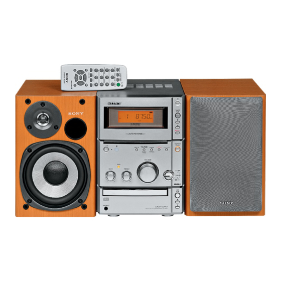
CMT-CPX1
HCD-CPX1
SS-CPX1
240.5 × 291
×
×
CMT-CPX1
ACCESSORIES
Part No.
Description
1-477-715-11
COMMANDER, STANDARD (RM-SMR1)
1-754-059-12
ANTENNA, LOOP (AM)
1-793-184-22
CONNECTOR (F TYPE ADAPTOR) (FM)
4-210-254-02
CUSHION (FOOT) (for SS-CPX1)
4-228-952-01
COVER, BATTERY (for RM-SMR1)
4-244-991-11
MANUAL, INSTRUCTION (ENGLISH)
4-244-991-21
MANUAL, INSTRUCTION (FRENCH) (US, Canadian)
4-244-991-31
MANUAL, INSTRUCTION (FRENCH, SPANISH)
4-244-991-41
MANUAL, INSTRUCTION (TRADITIONAL CHINESE)
4-244-991-51
MANUAL, INSTRUCTION (KOREAN) (Korean)
MICRO Hi-Fi COMPONENT SYSTEM
US Model
Canadian Model
E Model
Australian Model
Remark
(Singapore)
(Singapore)
Table of Contents

Related Manuals for Sony SS-CPX1


Summary of Contents for Sony SS-CPX1
- Page 1 1-477-715-11 COMMANDER, STANDARD (RM-SMR1) SPEAKER SYSTEM SS-CPX1 1-754-059-12 ANTENNA, LOOP (AM) 1-793-184-22 CONNECTOR (F TYPE ADAPTOR) (FM) 4-210-254-02 CUSHION (FOOT) (for SS-CPX1) 4-228-952-01 COVER, BATTERY (for RM-SMR1) SPECIFICATIONS 4-244-991-11 MANUAL, INSTRUCTION (ENGLISH) Power requirements 4-244-991-21 MANUAL, INSTRUCTION (FRENCH) (US, Canadian)
- Page 2 CMT-CPX1 REVISION HISTORY Clicking the version allows you to jump to the revised page. Also, clicking the version at the upper right on the revised page allows you to jump to the next revised page. Ver. Date Description of Revision 2003.04...
- Page 3 CD: 2 Hz – 20 kHz without notice. DIN power output (rated): 55 + 55 W Wavelength 780 – 790 nm (4 ohms at 1 kHz, DIN) COMPACT DISC DECK RECEIVER Sony Corporation 9-877-173-01 2003D0500-1 Home Audio Company C 2003.04 Published by Sony Engineering Corporation...
- Page 4 OPERATION. REPLACE THESE COMPONENTS WITH DE FONCTIONNEMENT. NE REMPLACER CES COM- SONY PARTS WHOSE PART NUMBERS APPEAR AS POSANTS QUE PAR DES PIÈCES SONY DONT LES SHOWN IN THIS MANUAL OR IN SUPPLEMENTS PUB- NUMÉROS SONT DONNÉS DANS CE MANUEL OU LISHED BY SONY.
-
Page 5: Table Of Contents
HCD-CPX1 TABLE OF CONTENTS SERVICING NOTES EXPLODED VIEWS ..........4 7-1. Case Section ..............47 GENERAL 7-2. Front Panel Section-1 ............48 7-3. Front Panel Section-2 ............49 Location of Controls ............8 7-4. Lid (TC) Section ............. 50 Setting the Clock ............. 9 7-5. -
Page 6: Servicing Notes
HCD-CPX1 SECTION 1 SERVICING NOTES MODEL IDENTIFICATION NOTES ON HANDLING THE OPTICAL PICK-UP – Back Panel – BLOCK OR BASE UNIT The laser diode in the optical pick-up block may suffer electro- static break-down because of the potential difference generated by the charged electrostatic load, etc. - Page 7 HCD-CPX1 TAPE MECHANICAL DECK SERVICE POSITION Set up the service position with putting an insulator under the mechanical deck as the figure shown below. tape mechanical deck insulator CD MECHANISM DECK SERVICE POSITION Set up the service position for the CD mechanism deck with disassembling the entire set as the figure shown below. main board front panel AMP section...
- Page 8 HCD-CPX1 NOTE ON LEADING THE WIRE (FLAT TYPE) (9 CORE) Lead the wire (flat type) (9 core) properly to prevent the wire from coming out from the right side of the guides on the sub panel or sagging inside of the lid. lid (TC) guides wire (flat type) (9 core)
- Page 9 HCD-CPX1 CLINCHING THE WIRE (FLAT TYPE) (21 CORE) AMP board heat sink Clinch the wire (flat type) (21 core) to prevent the wire from contacting with the heat sink of the AMP board. HANDLING TWO CABLES FROM THE SUB POWER AND THE SWITCHING REGULATOR TO THE MAIN BOARD Note: Fix two cables with the lead pin and the fabric non woven (10 –...
-
Page 10: General
HCD-CPX1 SECTION 2 This section is extracted from instruction manual. GENERAL • LOCATION OF CONTROLS – Front View – BUTTON DESCRIPTIONS ALPHABETICAL ORDER ?/1 (power) 1 R – Z A – Q TAPE Z (eject) 4 Remote sensor 2 BASS +/– wa TAPE nN (play) 5 REPEAT qs CD SYNCHRO qa... -
Page 11: Setting The Clock
HCD-CPX1 – Remote Control – ALPHABETICAL ORDER BUTTON DESCRIPTIONS ?/1 (power) 4 A – E F – Z TAPE nN (play) 7 CD ws FUNCTION wg TAPE x (stop) 8 CLEAR w; PLAY MODE wa CD NX (play pause) 0 CLOCK/TIMER SELECT 2 REPEAT qs CD x (stop) qa... -
Page 12: Disassembly
HCD-CPX1 SECTION 3 DISASSEMBLY • This set can be disassembled in the order shown below. 3-1. DISASSEMBLY FLOW 3-2. CASE (Page 11) 3-3. FRONT PANEL SECTION (Page 11) 3-4. TC BOARD, MECHANICAL DECK 3-5. MAIN BOARD (Page 12) (Page 12) 3-6. -
Page 13: Case
HCD-CPX1 Note: Follow the disassembly procedure in the numerical order given. 3-2. CASE 4 case 2 three screws (BVTP3 × 1 two case screws 1 two case screws 3-3. FRONT PANEL SECTION 3 wire (flat type) (19 core) (CN221) 1 screw (BVTP3 ×... -
Page 14: Tc Board, Mechanical Deck
HCD-CPX1 3-4. TC BOARD, MECHANICAL DECK 2 wire (flat type) (8 core) 6 four screws (CN602) 1 wire (flat type) (19 core) (BVTP3 × (CN603) Note: Must not use a magnetic screwdriver to prevent the screws from being magnetized. 7 ground wire lead 4 three screws (PTPWH 2) 5 TC board... -
Page 15: Tuner Unit
HCD-CPX1 3-6. TUNER UNIT 3 bracket 2 two screws (BVTP3 × 1 connector (CN990) 5 two screws (BVTP3 × 6 tuner unit 4 wire (flat type) (11 core) 2 two screws (BVTP3 × 3-7. CD MECHANISM DECK (CDM55A-K6BD44S) 1 two claws 2 CD lid 3 screw 9 CD mechanism deck... -
Page 16: Loading Board
HCD-CPX1 3-8. LOADING BOARD 2 belt (CDM55) 3 Pull the tray (CDM55D) pushing B . 1 Rotate the gear(A) in the direction of arrow A . 5 loading board 4 two screws (BTP2.6 × 8) 3-9. CAM (CDM55) 3 spacer (55) 4 pulley (LDG) 6 gear (A) 5 gear (B) -
Page 17: Base Unit (Bu-K6Bd44S)
HCD-CPX1 3-10. BASE UNIT (BU-K6BD44S) 6 base unit (BU-K6BD44S) 1 two floating screws (PTPWHM2.6) 2 two screws (BTTP M2.6) 3 two stoppers (BU) 5 two insulators 5 two insulators 3-11. MOTOR GEAR ASSY (SLED) (M102), BD BOARD 6 gear (A) 5 claw 7 gear (B) 8 two screws... -
Page 18: Optical Pick-Up (Kss-213D)
HCD-CPX1 3-12. OPTICAL PICK-UP (KSS-213D) 3 Remove the optical pick-up (KSS-213D) in the direction of arrow B . 2 sled shaft 1 Slide the lever in the direction of arrow A . -
Page 19: Test Mode
HCD-CPX1 SECTION 4 TEST MODE [CMN (MC) TEST MODE] [SHIP MODE (NO MEMORY CLEAR) ] • This mode is used to check operations of Amplifier. • This mode moves the optical pick-up to the position durable to Procedure: vibration. Use this mode when returning the set to the customer 1. - Page 20 HCD-CPX1 [AGING MODE] 3. Tape Deck Section The sequence during the aging mode is following as below. • This mode can be used for operation check of CD section and If an error occurred, stop display that step. tape deck section. Display at the aging mode is “TAPE AG—”.
-
Page 21: Deck Section
HCD-CPX1 SECTION 5 ELECTRICAL ADJUSTMENTS REC LEVEL ADJUSTMENT DECK SECTION 0 dB=0.775 V Procedure: [FUNCTION] 1. Press the key to select “MD” or “VIDEO”. Note: Confirm each contents of this section first of all. If the results are not satisfied, do the adjustment. 2. -
Page 22: Cd Section
HCD-CPX1 Checking Location: CD SECTION – BD BOARD (Conductor Side) – Note: CD Block is basically constructed to operate without adjustment. Use YEDS-18 disc (3-702-101-01) unless otherwise indicated. Use an oscilloscope with more than 10 MΩ impedance. Clean the object lens by an applicator with neutral detergent when the signal level is low than specified value with the following checks. -
Page 23: Diagrams
HCD-CPX1 SECTION 6 DIAGRAMS 6-1. BLOCK DIAGRAM – CD SERVO Section – FILTER DIGITAL SIGNAL PROCESSOR, DIGITAL FILTER, D/A CONVERTER IC101 (1/2) RF AMP, 56 53 FOCUS/TRACKING ERROR AMP IC103 A+3.3V PCMD LRCK INTERFACE RFAC C2PO RFAC RFAC RFAC ASYMMETRY DIGITAL SUMMING DEMODULATOR... -
Page 24: Block Diagram - Tuner/Tape Deck Section
HCD-CPX1 6-2. BLOCK DIAGRAM – TUNER/TAPE DECK Section – ANTENNA TUNER UNIT TUNER L-CH (Page 23) FM ANT L-CH FM 75Ω COAXIAL ANT GND R-CH R-CH AM ANT ST DOUT ANT GND ST DIN ST CLK ST CE MUTING ST MUTE TUNED TUNED STEREO... -
Page 25: Block Diagram - Main Section
HCD-CPX1 6-3. BLOCK DIAGRAM – MAIN Section – J801 R-CH HEADPHONE AMP PHONES IC102 HEADPHONE TUNER +9V, RIPPLE FILTER MUTING TC A+9V Q180, 181 Q182 L-CH R-CH (Page 22) MUTING L-CH CONTROL SWITCH (Page 21) Q184, 185 L-CH A/D CONVERTER DIGITAL AUDIO POWER AMP (Page 22) -
Page 26: Block Diagram - Display/Power Supply Section
HCD-CPX1 6-4. BLOCK DIAGRAM – DISPLAY/POWER SUPPLY Section – D801 LIQUID CRYSTAL LED DRIVE LED STANDBY (STANDBY) DISPLAY DRIVER Q801 IC803 D802 LED DRIVE LED DSG Q802 5 LCD DATA LIQUID CRYSTAL 7 LCD CLK D803 LED DRIVE DISPLAY 6 LCD CS LED CD 79 LCD801 Q803... -
Page 27: Note For Printed Wiring Boards And Schematic Diagrams
HCD-CPX1 6-5. NOTE FOR PRINTED WIRING BOARDS AND SCHEMATIC DIAGRAMS • Circuit Boards Location Note on Printed Wiring Board: Note on Schematic Diagram: • X : parts extracted from the component side. • All capacitors are in µF unless otherwise noted. pF: µµF AMP board •... -
Page 28: Printed Wiring Board - Bd Board
HCD-CPX1 6-6. PRINTED WIRING BOARD – BD Board – • See page 25 for Circuit Boards Location. :Uses unleaded solder. S101 (LIMIT) ON : WHEN THE OPTICAL PICK-UP M101 IS INNER POSITION BD BOARD (SPINDLE) C159 JW621 JR101 R159 JW609 R158 R197 C146... -
Page 29: Schematic Diagram - Bd Board
HCD-CPX1 6-7. SCHEMATIC DIAGRAM – BD Board – • • See page 30 for Waveforms. See page 40 for IC Block Diagrams. R196 2.2k R195 330k R194 C193 C194 C109 C111 R109 C198 1500p 100p C116 C183 C184 C185 C165 C146 C130 JR101... -
Page 30: Printed Wiring Board - Tc Board
HCD-CPX1 6-8. PRINTED WIRING BOARD – TC Board – • See page 25 for Circuit Boards Location. :Uses unleaded solder. • Semiconductor Location MAIN BOARD Ref. No. Location TAPE DECK BLOCK CN211 TC BOARD SUPPLIED WITH THE D681 (Page 31) ASSEMBLED BLOCK CN603 IC601... -
Page 31: Schematic Diagram - Tc Board
HCD-CPX1 6-9. SCHEMATIC DIAGRAM – TC Board – • See page 30 for Waveform. REC/PB SWITCHING R602 R604 C607 R609 4.7k 470p 2.2k IC602 CN602 BA3126N RV602 PLAY SW R REC F REC TAPE DECK BLOCK R611 PACK SUPPLIED WITH M+10V THE ASSEMBLED TRGM+... - Page 32 HCD-CPX1 • Waveforms – TC Board – – MAIN Board – – BD Board – – AMP Board – – LCD Board – ra IC803 3 (OSC2) 1 IC103 qg (RFAC) (CD play mode) 5 IC101 rd (RFDC) (CD play mode) qa Q642, 643 (Collector) (REC mode) wa IC401 qa (XCOUT) ea IC603 q;...
-
Page 33: Printed Wiring Boards - Loading/Main Boards
HCD-CPX1 6-10. PRINTED WIRING BOARDS – LOADING/MAIN Boards – • See page 25 for Circuit Boards Location. :Uses unleaded solder. • Semiconductor Location (Page 28) TC BOARD CN603 MAIN BOARD Ref. No. Location R491 D301 JW364 R556 R451 R448 R449 R555 R490 R554... -
Page 34: Schematic Diagram - Main Board (1/2)
HCD-CPX1 6-11. SCHEMATIC DIAGRAM – MAIN Board (1/2) – • See page 40 for IC Block Diagram. (1/2) CN221 M+11.5V MGND TC TRIG TC CAPM +3.3V C108 R103 TC END-SW 0.0027 3.9k TC HALF-REC D302 TC PLAY C102 C106 1SS355TE C111 R133 R132... -
Page 35: Schematic Diagram - Loading/Main (2/2) Boards
HCD-CPX1 6-12. SCHEMATIC DIAGRAM – LOADING/MAIN (2/2) Boards – • • See page 30 for Waveforms. See page 40 for IC Block Diagram. (2/2) BACK LIGHT +7V LED GND LCD RESET LCD CLK LCD DATA Q433 C432 DTA123YKA LCD CS B+ SWITCH LCD C/D (Page 37) -
Page 36: Printed Wiring Board - Amp Board
HCD-CPX1 6-13. PRINTED WIRING BOARD – AMP Board – • See page 25 for Circuit Boards Location. :Uses unleaded solder. AMP BOARD (COMPONENT SIDE) AMP BOARD (CONDUCTOR SIDE) D662 D660 C690 R610 FB610 C613 C661 C649 C652 R609 (CHASSIS) (CHASSIS) EP602 C674 EP601... -
Page 37: Schematic Diagram - Amp Board
HCD-CPX1 6-14. SCHEMATIC DIAGRAM – AMP Board – • • See page 30 for Waveforms. See page 40 for IC Block Diagrams. CN601 DIAGNOSTIC SP-RELAY ENABLE DGND D+6.2V DGND D+5V R601 FB601 SCDT R602 SC SHIFT R603 EP601 SC LATCH DGND R604 C674... -
Page 38: Printed Wiring Boards - Back Light/Lcd/Switch Boards
HCD-CPX1 6-15. PRINTED WIRING BOARDS – BACK LIGHT/LCD/SWITCH Boards – • See page 25 for Circuit Boards Location. :Uses unleaded solder. • Semiconductor Location Ref. No. Location S804 D801 (CD) D802 R814 D803 D804 S806 D805 (CD) D806 R815 C815 D807 D808 S805... -
Page 39: Schematic Diagram - Back Light/Lcd/Switch Boards
HCD-CPX1 6-16. SCHEMATIC DIAGRAM – BACK LIGHT/LCD/SWITCH Boards – • • See page 30 for Waveform. See page 40 for IC Block Diagram. RV803 RV802 RV801 ROTARY ENCODER ROTARY ENCODER ROTARY ENCODER LCD801 BASS TREBLE VOLUME LIQUID CRYSTAL DISPLAY REMOTE CONTROL RECEIVER C810... -
Page 40: Printed Wiring Boards - Hp/Sp Out/Power Boards
HCD-CPX1 6-17. PRINTED WIRING BOARDS – HP/SP OUT/SUB POWER Boards – • See page 25 for Circuit Boards Location. :Uses unleaded solder. (CHASSIS) HP BOARD MAIN BOARD CN102 (Page 31) FB803 C820 EP801 NO805 C817 FB801 1-686-793- (21) J801 FB802 PHONES C818 SUB POWER BOARD... -
Page 41: Schematic Diagram - Hp/Sp Out/Power Boards
HCD-CPX1 6-18. SCHEMATIC DIAGRAM – HP/SP OUT/SUB POWER Boards – FB801 CN701 Lch-1 C817 NO805 L721 0.001 FB706 Lch-2 C701 HP DET 470p J801 HP R (Page 35) PHONES C818 C702 0.001 HP GND 470p FB707 HP L J701 L731 C820 FB802 (Page 33) - Page 42 HCD-CPX1 • IC Block Diagrams – BD Board – IC101 CXD3017Q IC103 CXA2647N-T4 ROM/RW DC OFST RFDCI – – ERROR RFDC DIGITAL CORRECTOR ASYMMETRY DIGITAL CORRECTOR OPERATIONAL LRCK AMPLIFIER ANALOG SWITCH PCMD INTERFACE DEMODULATOR – ROM/RW VOFST CONVERTER EMPH XVDD XTAI TIMING XTAO...
- Page 43 HCD-CPX1 – MAIN Board – IC101 LC75342 23 22 21 20 19 18 17 – CONTROL CIRCUIT LOGIC INTERFACE CIRCUIT – – CONTROL – CIRCUIT 11 12 13 14 IC201 BA6956AN CONTROL LOGIC – AMP Board – IC600 CXD9743N 41 40 39 38 36 35 34 33 31 30 29 LINER...
- Page 44 HCD-CPX1 IC618 NJM2870F18 (TE2) IC650, 680 CXD9750L VBBA VBBA VBOOTA VDRVA VDRVA UNDER THERMAL VDDA VOLTAGE SHUT DOWN LOCK–OUT GNDA THERMAL PROTECTION BANDGAP DIAGA REFERENCE PROTECTOR CIRCUIT CROSS OVER DELAY FILTER LOW SIDE HIGH SIDE LEVEL SHIFT LEVEL SHIFT DRIVER DRIVER VBBA VDRVA...
- Page 45 HCD-CPX1 IC603 PCM1802DBR SINGLE-END/ 5TH ORDER MODE1 VINL 1 DIFFERENTIAL DELTA-SIGMA MODE0 CONVERTER MODULATOR FMT1 VINR 2 FMT0 x16 1/64 SERIAL (x1/128) DECIMATION INTERFACE VREF1 3 SCKI REFERENCE FILTER & VREF2 4 MODE/FORMAT WITH DGND DC CUT CONTROL FILTER DOUT SINGLE-END/ 5TH ORDER DIFFERENTIAL...
-
Page 46: Ic Pin Function Description
HCD-CPX1 6-19. IC PIN FUNCTION DESCRIPTION • MAIN BOARD IC401 M30622MGN-B08FP (SYSTEM CONTROLLER (CD MECHANISM CONTROL)) Pin No. Pin Name Description LCD ON Power on/off control signal output for liquid crystal display “H”: power on RDS DATA Serial data input from the RDS decoder Not used Signal output for discriminating between command and display data to the liquid crystal display LCD CD driver “L”: display data, “H”: command... - Page 47 HCD-CPX1 Pin No. Pin Name Description LED STANDBY LED drive signal output of the standby indicator “H”: LED on SC DT Serial data output to the digital audio signal processor SC SHIFT Serial data shift clock signal output to the digital audio signal processor SC LATCH Serial data latch pulse signal output to the digital audio signal processor NSP MUTE...
- Page 48 HCD-CPX1 Pin No. Pin Name Description TC END SW Tape end detect switch input terminal Recording-proof claw (forward/reverse) detect switch and cassette in detect switch input terminal TC HALF/REC/SW (A/D input) MODEL Model setting terminal DEST Destination setting terminal 94, 95 KEY3, KEY2 Front panel key input terminal (A/D input) AVSS...
-
Page 49: Exploded Views
HCD-CPX1 SECTION 7 EXPLODED VIEWS NOTE: • -XX and -X mean standardized parts, so they • Items marked “*” are not stocked since they The components identified by mark 0 or dotted line with mark 0 are may have some difference from the original are seldom required for routine service. -
Page 50: Front Panel Section-1
HCD-CPX1 7-2. FRONT PANEL SECTION-1 not supplied not supplied lid (TC) section front panel section-2 Ref. No. Part No. Description Remark Ref. No. Part No. Description Remark 4-244-021-01 SPRING (LID TC), TORSION 4-244-014-01 LEVER (EJECT) 1-796-456-31 DECK, MECHANICAL 4-244-023-01 SPRING (EJECT), COMPRESSION A-4731-316-A TC BOARD, COMPLETE 4-244-012-01 BUTTON (EJECT) 1-824-192-11 WIRE (FLAT TYPE) (8 CORE) -
Page 51: Front Panel Section-2
HCD-CPX1 7-3. FRONT PANEL SECTION-2 not supplied not supplied not supplied (HP board) Ref. No. Part No. Description Remark Ref. No. Part No. Description Remark 4-240-765-11 KNOB, TUNING 4-951-620-01 SCREW (2.6X8), +BVTP 4-240-764-11 KNOB, VOLUME 4-244-006-01 BAND (UPPER), DIVISION 4-240-763-11 KNOB, BASS 4-233-372-02 FOOT (FELT) X-4955-234-2 PANEL ASSY, FRONT (US, CND) 4-240-771-11 SUPPORT, TUNING... -
Page 52: Lid (Tc) Section
X-4955-604-1 LID (TC) (C) ASSY 4-951-620-01 SCREW (2.6X8), +BVTP 4-236-666-01 CUSHION (LCD) 4-244-007-01 HOLDER (TC) 4-244-026-01 SHEET, DIFFUSION 4-244-022-01 SPRING (TC), LEAF 4-244-009-01 PLATE, LIGHT GUIDE 4-925-161-81 EMBLEM (4-A), SONY 1-769-916-11 WIRE (FLAT TYPE) (9 CORE) 7-685-234-14 SCREW +KTP 2.6X8 TYPE2NON-SLIT 1-686-791-11 LCD BOARD... -
Page 53: Chassis Section-1
HCD-CPX1 7-5. CHASSIS SECTION-1 not supplied chassis section-2 Ref. No. Part No. Description Remark Ref. No. Part No. Description Remark A-4731-299-A MAIN BOARD, COMPLETE (SP, KR) 7-685-645-79 SCREW +BVTP 3X6 TYPE2 TT (B) A-4731-302-A MAIN BOARD, COMPLETE (US, CND) 7-685-646-79 SCREW +BVTP 3X8 TYPE2 TT (B) A-4733-555-A MAIN BOARD, COMPLETE (AUS) -
Page 54: Chassis Section-2
HCD-CPX1 7-6. CHASSIS SECTION-2 chassis section-3 not supplied CDM55A-K6BD44S not supplied The components identified by Les composants identifiés par une mark 0 or dotted line with marque 0 sont critiques pour la mark 0 are critical for safety. sécurité. Replace only with part num- Ne les remplacer que par une pièce ber specified. -
Page 55: Chassis Section-3
HCD-CPX1 7-7. CHASSIS SECTION-3 not supplied not supplied not supplied (SP out board) not supplied not supplied The components identified by Les composants identifiés par une mark 0 or dotted line with marque 0 sont critiques pour la mark 0 are critical for safety. sécurité. -
Page 56: Cd Mechanism Deck Section (Cdm55A-K6Bd44S)
HCD-CPX1 7-8. CD MECHANISM DECK SECTION (CDM55A-K6BD44S) not supplied M201 not supplied BU-K6BD44S Ref. No. Part No. Description Remark Ref. No. Part No. Description Remark 4-925-315-31 DAMPER A-4735-082-A MAGNET ASSY 4-224-894-22 TRAY (CDM55D) 4-231-777-02 SHEET (KH2) 1-674-336-12 LOADING BOARD 4-218-252-31 SCREW (+PTPWH M2.6), FLOATING 4-220-229-02 LEVER (SW) 4-229-358-01 SHAFT (BU21) 4-985-672-01 SCREW (+PTPWH M2.6), FLOATING... -
Page 57: Base Unit (Bu-K6Bd44S)
HCD-CPX1 7-9. BASE UNIT SECTION (BU-K6BD44S) M101 M102 The components identified by Les composants identifiés par une mark 0 or dotted line with marque 0 sont critiques pour la mark 0 are critical for safety. sécurité. Replace only with part num- Ne les remplacer que par une pièce ber specified. -
Page 58: Electrical Parts List
HCD-CPX1 SECTION 8 ELECTRICAL PARTS LIST NOTE: • Due to standardization, replacements in the • Items marked “*” are not stocked since they The components identified by 0 or dotted line with mark mark parts list may be different from the parts speci- are seldom required for routine service. - Page 59 HCD-CPX1 BACK LIGHT Ref. No. Part No. Description Remark Ref. No. Part No. Description Remark < DIODE > L670 1-424-777-11 INDUCTOR 10uH D611 8-719-988-61 DIODE 1SS355TE-17 < TRANSISTOR > D621 8-719-988-61 DIODE 1SS355TE-17 D650 6-500-131-01 DIODE LI116 Q691 8-729-602-36 TRANSISTOR 2SA1602-F D651 6-500-248-01 DIODE SFPL-62V...
- Page 60 HCD-CPX1 BACK LIGHT Ref. No. Part No. Description Remark Ref. No. Part No. Description Remark < LED > C198 1-104-665-11 ELECT 100uF D806 8-719-075-50 LED SELS6B14C-TP5 (LCD BACK LIGHT) < CONNECTOR > D807 8-719-075-50 LED SELS6B14C-TP5 (LCD BACK LIGHT) D808 8-719-075-50 LED SELS6B14C-TP5 (LCD BACK LIGHT) CN101 1-569-914-11 SOCKET, CONNECTOR 21P...
- Page 61 HCD-CPX1 LOADING MAIN Ref. No. Part No. Description Remark Ref. No. Part No. Description Remark < LIQUID CRYSTAL DISPLAY > R192 1-216-839-11 METAL CHIP 1/10W R193 1-216-847-11 METAL CHIP 150K 1/10W LCD801 1-805-113-11 DISPLAY PANEL, LIQUID CRYSTAL R194 1-216-843-11 METAL CHIP 1/10W R195 1-216-851-11 METAL CHIP...
- Page 62 HCD-CPX1 MAIN Ref. No. Part No. Description Remark Ref. No. Part No. Description Remark C152 1-126-960-11 ELECT C501 1-126-964-11 ELECT 10uF C153 1-126-960-11 ELECT C502 1-130-495-00 MYLAR 0.1uF C154 1-126-960-11 ELECT C155 1-126-960-11 ELECT C503 1-130-495-00 MYLAR 0.1uF C156 1-126-960-11 ELECT <...
- Page 63 HCD-CPX1 MAIN Ref. No. Part No. Description Remark Ref. No. Part No. Description Remark IC303 8-759-071-48 IC TA7807S R174 1-216-837-11 METAL CHIP 1/10W IC304 8-759-394-36 IC BA09T (US, CND) IC304 8-759-701-59 IC NJM78M09FA (SP, KR, AUS) R175 1-216-805-11 METAL CHIP 1/10W IC401 6-802-524-01 IC M30622MGN-B08FP...
- Page 64 HCD-CPX1 MAIN SP OUT SUB POWER Ref. No. Part No. Description Remark Ref. No. Part No. Description Remark R450 1-216-809-11 METAL CHIP 1/10W R565 1-216-833-11 METAL CHIP 1/10W R451 1-216-809-11 METAL CHIP 1/10W R566 1-216-833-11 METAL CHIP 1/10W R452 1-216-809-11 METAL CHIP 1/10W R567 1-216-833-11 METAL CHIP...
- Page 65 HCD-CPX1 SUB POWER SWITCH Ref. No. Part No. Description Remark Ref. No. Part No. Description Remark < TRANSISTOR > < RESISTOR > Q990 8-729-141-73 TRANSISTOR 2SC3624A-T1L15L16 R812 1-216-821-11 METAL CHIP 1/10W (SP, KR, AUS) R813 1-216-825-11 METAL CHIP 2.2K 1/10W Q991 8-729-141-73 TRANSISTOR 2SC3624A-T1L15L16...
- Page 66 HCD-CPX1 Ref. No. Part No. Description Remark Ref. No. Part No. Description Remark C604 1-130-495-00 MYLAR 0.1uF < TRANSISTOR > C605 1-126-964-11 ELECT 10uF C606 1-126-960-11 ELECT Q639 8-729-119-77 TRANSISTOR 2SA1175-FEK Q640 8-729-029-66 TRANSISTOR DTC114ESA C607 1-162-962-11 CERAMIC CHIP 470PF Q641 8-729-801-93 TRANSISTOR 2SD1387...
- Page 67 HCD-CPX1 Ref. No. Part No. Description Remark Ref. No. Part No. Description Remark R689 1-216-829-11 METAL CHIP 4.7K 1/10W R690 1-216-829-11 METAL CHIP 4.7K 1/10W R691 1-216-833-11 METAL CHIP 1/10W R692 1-216-829-11 METAL CHIP 4.7K 1/10W R693 1-216-841-11 METAL CHIP 1/10W R694 1-216-837-11 METAL CHIP...
- Page 68 HCD-CPX1 REVISION HISTORY Clicking the version allows you to jump to the revised page. Also, clicking the version at the upper right on the revised page allows you to jump to the next revised page. Ver. Date Description of Revision 2003.04...