Sony SMP-N100 Service Manual
Network media player
Hide thumbs
Also See for SMP-N100:
- Operating instructions manual (63 pages) ,
- Specifications (1 page) ,
- Instruction & operation manual (14 pages)
Table of Contents
Quick Links
SERVICE MANUAL
Ver. 1.0 2010.07
Inputs and outputs
(Jack name:
Jack type/Output level/Load impedance)
LINE OUT R-AUDIO-L:
Phono jack/2 Vrms/10 kilohms
DIGITAL OUT (OPTICAL):
Optical output jack/–18 dBm
(wave length 660 nm)
HDMI OUT:
HDMI 19-pin standard connector
COMPONENT VIDEO OUT
(Y, P
, P
):
B
R
Phono jack/Y: 1.0 Vp-p/
P
, P
: 0.7 Vp-p/75 ohms
B
R
LINE OUT VIDEO:
Phono jack/1.0 Vp-p/75 ohms
LAN (100):
100BASE-TX Terminal
*Except Russian
*Russian ONLY
9-890-736-11
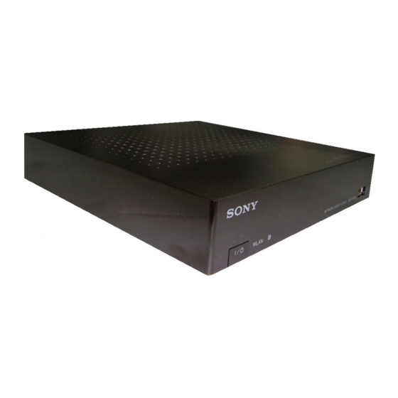
1 Photo : SMP-N100
Remote : RMT-D301
SPECIFICATIONS
USB:
USB jack Type A (For connecting a USB
memory, hard disk drive, memory card
reader, digital still camera, and digital video
camera)
DC IN:
12 V DC
Wireless
Wireless LAN standard:
IEEE802.11/b/g/n (Except Russian)
IEEE802.11/b/g (Russian ONLY)
Frequency range:
US:
2.4GHz band: Channels 1-11
CANADIAN:
2.4GHz band: Channels 1-11
AEP, UK, RUSSIAN:
2.4GHz band: Channels 1-13
Modulation:
DS-SS Modem and OFDM Modem
Sony Corporation
Home Entertainment Business Group
SMP-N100
Canadian Model
Russian Model
General
Power requirements:
AC adapter: 110 – 240 V AC, 50/60 Hz
Power consumption (approx.):
14 W
Dimensions (approx.):
185 mm × 193 mm × 40 mm
(17
3
/
in. × 7
8
(width/depth/height) incl. projecting parts
Mass (approx.):
680 g (1 lb 8 oz)
Operating temperature:
5 ºC to 35 ºC (41 °F to 95 °F)
Operating humidity:
25 % to 80 %
Supplied accessor ies
• Audio/video cable (phono plug ×3) (1)
• AC power cord (1)
• AC adapter (1)
• Remote control (remote) (1)
• Size AA (R6) batteries (2)
Specifications and design are subject to change
without notice.
NETWORK MEDIA PLAYER
Published by Design Engineering Dept.
RMT-D301
AEP Model
UK Model
US Model
5
/
in. × 1
5
/
in.)
8
8
2010G6900-1
© 2010.07
Table of Contents

Related Manuals for Sony SMP-N100


Summary of Contents for Sony SMP-N100
- Page 1 RMT-D301 SERVICE MANUAL AEP Model Canadian Model Russian Model Ver. 1.0 2010.07 UK Model US Model 1 Photo : SMP-N100 Remote : RMT-D301 SPECIFICATIONS Inputs and outputs General USB: Power requirements: USB jack Type A (For connecting a USB (Jack name: AC adapter: 110 –...
- Page 2 Ordinary soldering irons can be used but the iron tip has to be applied to the solder joint for a slightly longer time. Soldering irons using a temperature regulator should be set to IN SUPPLEMENTS PUBLISHED BY SONY. about 350°C. Caution: The printed pattern (copper foil) may peel away if the...
-
Page 3: Table Of Contents
SMP-N100 TABLE OF CONTENTS Section Title Page Section Title Page SERVICE NOTE 1-1. USB HARNESS DRESSING 4-11 MB-136 BOARD (SATA) SCHEMATIC DIAGRAM (8/15) ....... 4-11 1-1-1 Keep distance the USB Harness from the Heatsink ... 1-1E 4-12 MB-136 BOARD (AUDIO) -
Page 4: Service Note
SMP-N100 SECTION 1 SERVICE NOTE 1-1. USB HARNESS DRESSING USB-017: 1-967-372-11 1-1-1. Keep distance the USB Harness from the Heatsink Keep the distance between the USB Harness and Heatsink 1-1-2. Keep distance the USB Harness from the Upper Chassis Use the Lead Pin to... -
Page 5: Disassembly
SMP-N100 SECTION 2 DISASSEMBLY 2-1. TOP COVER ASSY Note: Follow the disassembly procedure in the numerical order given. Top Cover Assy Five screws +BV3 (3-CR) Top Cover Three screws 3 One screw +BV3 (3-CR) SCREW +P 3X3... -
Page 6: Board, Fl200 And Wlan Card
SMP-N100 2-2. MB-136 Board, FL-200 and WLAN Card Five screws +BV3 (3-CR) MB-136 Board Flexible Flat Cable (MF-046) FL-200 Board One screw +BV3 (3-CR) Harness (USB-017) Wireless LAN Card Two screws +BV3 (3-CR) 2-3. Circuit Boards Location MB-136 Board FL-200 Board... -
Page 7: Block Diagrams
SMP-N100 SECTION 3 BLOCK DIAGRAMS 3-1. OVERALL BLOCK DIAGRAM (AC IN) IC1501 The components identifi ed by mark or dotted line with mark are critical for safety. Replace only with part number specifi ed. -
Page 8: Dsp Block Diagram
SMP-N100 3-2. DSP BLOCK DIAGRAM MB-136 BOARD DODQ0-DODQ15 FE_ RFIP IC104 FE_ RFIN 1Gb DDR2 DOA0-DOA12 FE_ RFIP2 SDRAM FE_ RFIN2 A_RBA0 BA0 - BA2 A_RBA1 FE_INA A_RBA2 FE_INB A_RRASB /RAS BB24 FE_INC A_RCASB /CAS AU23 FE_IND A_RWEB BC29 FE_INE... -
Page 9: Av Out Block Diagram
SMP-N100 3-3. AV OUT BLOCK DIAGRAM Q702 PG 3-4 CEC PULL-UP ISOLATING SWITCH IT-CON... -
Page 10: Usb/Ether/Wlan Block Diagram
SMP-N100 3-4. USB/ ETHER/ WLAN BLOCK DIAGRAM MB-136 BOARD CN603 IC1201 CN1201 LAN (100) X1201 25MHz MRESET IC1503 Front end circuit FL-200 BOARD CN3001 CN1102 S3001 GPIO4 AY10 GPIO2 CN1504 IC3001 VSTB GPIO5 AW11 GPIO1 CORE_RESETB GPIO6 AV12 D3002 D3001... -
Page 11: Power Block Diagram
SMP-N100 3-5. POWER BLOCK DIAGRAM 3-5E... -
Page 12: Schematic Diagrams
SMP-N100 SECTION 4 SCHEMATIC DIAGRAMS 4-1. THIS NOTE IS COMMON FOR SCHEMATIC DIAGRAMS • All capacitors are in µF unless otherwise noted. pF : µµF. 50V or less are not indicated except for electrolytics and tantalums. • All resistors are in ohms, 1/4 W (Chip resistors : 1 /10 W) un-less otherwise specified. -
Page 13: Frame Schematic Diagram
SMP-N100 4-2. FRAME SCHEMATIC DIAGRAM TO ETHERNET TO HDMI CN701 CN1201 MB-136 MF-049 USB-017 1-838-208-11 1-967-372-11 HARNESS CNXXX CN603 FL-200 WLAN CARD TO USB... - Page 14 SMP-N100 4-3. FL-200 BOARD (FRONT CONNECTOR) SCHEMATIC DIAGRAM - Ref. No.: FL-200 board; 20,000 series - • See page 5-2 for printed wiring board. FL-200 BOARD XX MARK:NO MOUNT IC3001 HM2140RS T-07M2 CN3001 JL3001 SIRCS JL3002 R3007 C3003 C3002 JL3003 C3001 6.3V...
- Page 15 SMP-N100 4-4. MB-136 BOARD (CXD9983GG/9984GG) SCHEMATIC DIAGRAM (1/15) • See page 5-3 for printed wiring board. - Ref. No.: MB-136 board; 10,000 series A SIDE B SIDE...
- Page 16 SMP-N100 4-5. MB-136 BOARD (CXD9983GG/9984GG) SCHEMATIC DIAGRAM (2/15) • See page 5-3 for printed wiring board. - Ref. No.: MB-136 board; 10,000 series A SIDE B SIDE...
-
Page 17: Board (Power1) Schematic Diagram
SMP-N100 4-6. MB-136 BOARD (POWER1) SCHEMATIC DIAGRAM (3/15) • See page 5-3 for printed wiring board. - Ref. No.: MB-136 board; 10,000 series... -
Page 18: Board (Clk/Power2) Schematic Diagram
SMP-N100 4-7. MB-136 BOARD (CLK/POWER2) SCHEMATIC DIAGRAM (4/15) • See page 5-3 for printed wiring board. - Ref. No.: MB-136 board; 10,000 series... -
Page 19: Board (Flash/Host) Schematic Diagram
SMP-N100 4-8. MB-136 BOARD (FLASH/HOST) SCHEMATIC DIAGRAM (5/15) • See page 5-3 for printed wiring board. - Ref. No.: MB-136 board; 10,000 series... -
Page 20: Board (Usb) Schematic Diagram
SMP-N100 4-9. MB-136 BOARD (USB ) SCHEMATIC DIAGRAM (6/15) • See page 5-3 for printed wiring board. - Ref. No.: MB-136 board; 10,000 series... -
Page 21: Board (Hdmi) Schematic Diagram
SMP-N100 4-10 . . MB-136 BOARD (HDMI ) SCHEMATIC DIAGRAM (7/15) • See page 5-3 for printed wiring board. - Ref. No.: MB-136 board; 10,000 series 4-10... -
Page 22: Board (Sata) Schematic Diagram
SMP-N100 4-11. MB-136 BOARD (SATA) SCHEMATIC DIAGRAM (8/15) • See page 5-3 for printed wiring board. - Ref. No.: MB-136 board; 10,000 series 4-11... -
Page 23: Board (Audio) Schematic Diagram
SMP-N100 4-12. MB-136 BOARD (AUDIO) SCHEMATIC DIAGRAM (9/15) • See page 5-3 for printed wiring board. - Ref. No.: MB-136 board; 10,000 series 4-12... -
Page 24: Board (Video) Schematic Diagram
SMP-N100 4-13. MB-136 BOARD (VIDEO ) SCHEMATIC DIAGRAM (10/15) • See page 5-3 for printed wiring board. - Ref. No.: MB-136 board; 10,000 series 4-13... -
Page 25: Board (Gpio/Jtag) Schematic Diagram
SMP-N100 4-14. MB-136 BOARD (GPIO/JTAG) SCHEMATIC DIAGRAM (11/15) • See page 5-3 for printed wiring board. - Ref. No.: MB-136 board; 10,000 series 4-14... -
Page 26: Board (Ethernet) Schematic Diagram
SMP-N100 4-15. MB-136 BOARD (ETHERNET) SCHEMATIC DIAGRAM (12 /15) • See page 5-3 for printed wiring board. - Ref. No.: MB-136 board; 10,000 series 4-15... -
Page 27: Board (Fe_Power/Sf/Sata) Schematic Diagram
SMP-N100 4-16 MB-136 BOARD (FE_POWER/SF/SATA) SCHEMATIC DIAGRAM (13 /15) • See page 5-3 for printed wiring board. - Ref. No.: MB-136 board; 10,000 series 4-16... -
Page 28: Board (Fe_Op/Motor Drive) Schematic Diagram
SMP-N100 4-17. MB-136 BOARD (FE_OP/MOTOR DRIVE) SCHEMATIC DIAGRAM (14 /15) • See page 5-3 for printed wiring board. - Ref. No.: MB-136 board; 10,000 series 4-17... -
Page 29: Board (Ifcon ) Schematic Diagram
SMP-N100 4-18. MB-136 BOARD (IFCON ) SCHEMATIC DIAGRAM (15 /15) • See page 5-3 for printed wiring board. - Ref. No.: MB-136 board; 10,000 series 4-18... - Page 30 SMP-N100 4-19. WAVEFORMS MB-136 BOARD IC1003 IC1003 (VIN) IC1003 (YOUT) 2.0Vp-p 1.2 Vp-p IC1003 (PYIN) (VOUT) IC1003 2.4 Vp-p 1.0 Vp-p IC1003 (PBIN) IC101 (NS_XTAL_I) 3.3 Vp-p 0.7Vp-p 27 MHz (PRIN) IC1003 (XTAL25MI) IC101 2.1 Vp-p 0.7Vp-p 25 MHz IC1003...
-
Page 31: Printed Wiring Boards
SMP-N100 SECTION 5 PRINTED WIRING BOARDS 5-1. THIS NOTE IS COMMON FOR PRINTED WIRING BOARDS • : Uses unleaded solders. • : Pattern from the side which enables seeing. (The other layers’ patterns are not indicated) Caution: Pattern face side:... -
Page 32: Board (Main)
SMP-N100 5-2. FL-200 (POWER SWITCH) PRINTED WIRING BOARD - Ref. No.: FL-200 board; 20,000 series - • See page 2-2 for circuit boards location. : Uses unleaded solder. There are a few cases that the part isn’t mounted in this model is printed on this diagram. - Page 33 SMP-N100 5-3. MB-136 BOARD (MAIN) PRINTED WIRING BOARD (SIDE A) • See page 2-2 for circuit boards location. There are a few cases that the part isn’t mounted in this model is printed on this diagram. - Ref. No.: MB-136 board; 10,000 series - : Uses unleaded solder.
- Page 34 SMP-N100 5-4. MB-136 BOARD (MAIN) PRINTED WIRING BOARD ( SIDE B ) • See page 2-2 for circuit boards location. There are a few cases that the part isn’t mounted in this model is printed on this diagram. - Ref. No.: MB-136 board; 10,000 series - : Uses unleaded solder.
-
Page 35: Ic Pin Function Description
SMP-N100 SECTION 6 IC PIN FUNCTION DESCRIPTION MAIN SYSTEM CONTROL PIN FUNCTION (MB-136 BOARD IC101: CXD9983GG/CXD9984GG) Symbol Type Description FESFDO Serial Data Input to Front_End Serial Flash VOUTD1 VOUTD5 VOUTD9 VOUTD12 VIND0 VIND12 VIND16 GPIO GPIO1 START-BIT SPDIF SPDIF Digital Audio Out... - Page 36 SMP-N100 AOMCLK Audio Out Master Clock AVDD12_APLL Power 1.2V Analog Power for APLL CH2_P Analog HDMI TX data 2 differential pair (P) CH0_P Analog HDMI TX data 0 differential pair (P) DACOUT6 Analog DAC Output AVDD33_VDACBG Power 3.3V Analog Power...
- Page 37 SMP-N100 VIND8 FORMAT1 VIND10 VIND18 SPDATA SPDIF in Serial Dat AOSDATA1 Audio Out Serial Data 1 AVSS33_XTAL Ground Analog Ground for XTAL AVSS33_HDMI Ground Analog Ground AVDD12_HDMI Power 1.2V Analog Power AVDD33_VDACY Power 3.3V Analog Power LCDRD Serial Interface Master Data Line (IF_SDI)
- Page 38 SMP-N100 FE_GIO8 GIO8 VCC3IO_1 Power 3.3V Digital IO Power NFALE NAND Flash address Latch Enable NFCEN2 NAND Flash 2nd Chip Enable NAND Flash Data INPUT/OUTPUT bit5 NFD5 NFD6 NAND Flash Data INPUT/OUTPUT bit6 FE_VWDC2O Analog Output FE_AUX1 Analog I/O Thermo- BU Temperature Monitor...
- Page 39 SMP-N100 VCCK Power 1.1V Digital Power VCCK Power 1.1V Digital Power VCCK Power 1.1V Digital Power VCCK_PWM Power 1.1V Digital Power for PWM VCCK Power 1.1V Digital Power VCCK Power 1.1V Digital Power VCC2IO Power 1.8V Digital IO Power B_RDQ18...
- Page 40 SMP-N100 AD28 DVSS Ground Digital Ground AD30 VCCK Power 1.1V Digital Power AD32 VCCK Power 1.1V Digital Power AD36 B_RBA1 Memory Bank Address bit 1 AD38 B_RA9 Memory Address bit 9 AD40 B_RBA0 Memory Bank Address bit 0 AD42 B_RCS_...
- Page 41 SMP-N100 AH40 B_RCAS_ Memory Column Address Strobe AH42 B_RA4 Memory Address bit 4 FE_XTAL25MO Output X'tal Output FE_XTAL25MI Input X'tal Input. The working frequency is 25Mhz Tray_is_in Input, A logical low Indicates the Tray is IN. Feedback Flag is from Tray...
- Page 42 SMP-N100 XO_RTC 32.768K Crystal OUT AVSS12_ADC Ground Analog Ground for SACD I/O, GIO_13 AT10 FE_GIO13 AT12 Slave I2C Clock AT14 DVSS Ground Digital Ground AT16 A_RDQ5 Memory Data bit 5 AT18 A_RDQM0 Memory Data Mask bit 0 AT20 A_RDQ11 Memory Data bit 11...
- Page 43 SMP-N100 AY18 VCC2IO Power 1.8V Digital IO Power AY20 A_RDQ8 Memory Data bit 8 AY22 VCC2IO Power 1.8V Digital IO Power AY24 A_RA4 Memory Address bit 4 AY26 VCC2IO Power 1.8V Digital IO Power AY28 A_RA10 Memory address bit 10...
-
Page 44: Service Mode
SMP-N100 SECTION 7 SERVICE MODE... - Page 45 SMP-N100...
- Page 46 SMP-N100...
- Page 47 SMP-N100...
- Page 48 SMP-N100...
- Page 49 SMP-N100...
- Page 50 SMP-N100...
- Page 51 SMP-N100...
- Page 52 SMP-N100...
- Page 53 SMP-N100 7-10...
- Page 54 SMP-N100 7-11E...
-
Page 55: Error Log List
SMP-N100 SECTION 8 ERROR LOG LIST... - Page 56 SMP-N100 8-2E...
-
Page 57: Troubleshooting
SMP-N100 SECTION 9 TROUBLESHOOTING Main Flowchart ..............9-2 Power (System) Flowchart ............ 9-3 IFcon Section Flowchart (1/2) ..........9-4 IFcon Section Flowchart (2/2) ..........9-5 Audio Section Flowchart ............9-6 Video Section Flowchart ............9-7 Ethernet Flowchart ..............USB (Front) Device Flowchart .......... - Page 58 SMP-N100...
- Page 59 SMP-N100...
- Page 60 SMP-N100...
- Page 61 SMP-N100...
- Page 62 SMP-N100...
- Page 63 SMP-N100...
- Page 64 SMP-N100...
- Page 65 SMP-N100...
- Page 66 SMP-N100 9-10...
- Page 67 SMP-N100 9-11...
- Page 68 SMP-N100 9-12E...
-
Page 69: Exploded Views
SMP-N100 SECTION 10 REPAIR PARTS LIST 10-1. EXPLODED VIEWS NOTE: The components identified by mark or dotted -XX and -X mean standardized parts, so they Items marked “*” are not stocked since they line with mark are critical for safety. -
Page 70: Accessories
SMP-N100 10-1-2. ACCESSORIES Cord, Connection (AV) Remote Commander AC Adaptor Power Supply Cord The components identified by mark Les composants identifiés par une or dotted line with mark marque sont critiquens pour la critical for safety. sécurité. Replace only with part number Ne les remplacer que par une pièce... -
Page 71: Electrical Parts List
SMP-N100 10-2 . ELECTRICAL PARTS LIST NOTE: or dotted line with mark are critical Due to standardization, replacements in the uA. . : µA. . uPA. . : µPA. . for safety. Replace only with part number uPB. . : µPB. . - Page 72 SMP-N100 Ref-No. Part No. Part Description R e m a r k s Ref-No. Part No. Part Description R e m a r k s C227 1-100-916-11 CERAMIC CHIP 0.1UF 10% 16V C135 1-100-916-11 CERAMIC CHIP 0.1UF 10% 16V C228 1-100-916-11 CERAMIC CHIP 0.1UF...
- Page 73 SMP-N100 Ref-No. Part No. Part Description R e m a r k s Ref-No. Part No. Part Description R e m a r k s C377 1-114-553-11 CERAMIC CHIP 10UF 10% 16V C1001 1-128-994-21 ELECT CHIP 47UF 20% 10V C378...
- Page 74 SMP-N100 Ref-No. Part No. Part Description R e m a r k s Ref-No. Part No. Part Description R e m a r k s Q305 6-552-430-01 TR DRC5114E0L FB605 1-400-580-21 FERRITE Q702 6-551-714-01 TRANSISTOR INK0001AC1-T112A-1 FL301 1-234-939-21 FILTER, EMI REMOVAL (SMD)
- Page 75 SMP-N100 Ref-No. Part No. Part Description R e m a r k s Ref-No. Part No. Part Description R e m a r k s R613 1-208-885-81 METAL CHIP 820 0.5% 1/16W R1139 1-218-965-81 METAL CHIP 10K 5% 1/16W R614 1-208-887-81 METAL CHIP 1K 0.5% 1/16W...
- Page 76 SMP-N100 Ref-No. Part No. Part Description R e m a r k s R1564 1-218-981-81 METAL CHIP 220K 5% 1/16W R1586 1-218-941-81 METAL CHIP 100 5% 1/16W R1615 1-208-911-81 METAL CHIP 10K 0.5% 1/16W MISCELLANEOUS PARTS R1616 1-208-911-81 METAL CHIP 10K 0.5% 1/16W...
- Page 77 SMP-N100 REVISION HISTORY Version Date Description of Revision 2010.07...