Table of Contents
Quick Links
Table of Contents

Related Manuals for Asus AAEON VPC-3350S

Summary of Contents for Asus AAEON VPC-3350S
- Page 1 VPC-3350S Mobile NVR User ’s Manual 5 Last Updated: October 19, 2021...
- Page 2 Copyright Notice This document is copyrighted, 2021. All rights are reserved. The orig inal manufacturer reserves the right to make improvements to the products described in this manual at any time without notice. No part of this manual may be reproduced, copied, translated, or transmitted in any form or by any means without the prior written permission of the original manufacturer.
- Page 3 Acknowledgement All other products’ name or trademarks are properties of their respective owners. Microsoft Windows is a registered trademark of Microsoft Corp. ⚫ Intel®, Pentium® and Celeron® are registered trademarks of Intel Corporation ⚫ Intel Atom™ is a trademark of Intel Corporation ⚫...
- Page 4 Packing List Before setting up your product, please make sure the following items have been shipped: I t em Quantity VPC-3350S DIMM Thermal Pad DIMM Sink SATA Cable SATA Power Cable If any of these items are missing or damaged, please contact your distributor or sales representative immediately.
- Page 5 About this Document This User’s Manual contains all the essential information, such as detailed descriptions and explanations on the product’s hardware and software features (if any), its specifications, dimensions, jumper/connector settings/definitions, and driver installation instructions (if any), to facilitate users in setting up their product. Users may refer to the product page at AAEON.com for the latest version of this document.
- Page 6 Saf e ty Precautions Please read the following safety instructions carefully. It is advised that you keep this manual for future references All cautions and warnings on the device should be noted. All cables and adapters supplied by AAEON are certified and in accordance with the material safety laws and regulations of the country of sale.
- Page 7 As most electronic components are sensitive to static electrical charge, be sure to ground yourself to prevent static charge when installing the internal components. Use a grounding wrist strap and contain all electronic components in any static-shielded containers. If any of the following situatio ns arises, please the contact our service personnel: Damaged power cord or plug Liquid intrusion to the device iii.
- Page 8 FCC Statement This device complies with Part 15 FCC Rules. Operation is subject to the following two conditions: (1) this device may not cause harmful interference, and (2) this device must accept any interference received including interference that may cause undesired operation. C aution: There is a danger of explosion if the battery is incorrectly replaced.
- Page 9 Chi na RoHS Requirements ( CN) 产品中有毒有害物质或元素名称及含量 AAEON System QO4-381 Rev.A0 有毒有害物质或元素 部件名称 铅 汞 镉 六价铬 多溴联苯 多溴二苯醚 (Pb) (Hg) (Cd) (Cr(VI)) (PBB) (PBDE) 印刷电路板 × ○ ○ ○ ○ ○ 及其电子组件 外部信号 × ○ ○ ○ ○ ○ 连接器及线材...
- Page 10 Chi na RoHS Requirement (EN) Hazardous and Toxic Materials List AAEON System QO4-381 Rev.A0 Hazardous or Toxic Materials or Elements Component Name PCB and Components Wires & Connectors for Ext.Connections Chassis CPU & RAM HDD Drive LCD Module Optical Drive Touch Control Module Batter y...
-
Page 11: Table Of Contents
Table of Contents Chapter 1 - Product Specifications ............. . . 1 Specifications .................... - Page 12 2.6.2 PER-T528 List of Jumpers............. 25 2.6.2.1 Reserved (CN4) ..............25 2.6.3 PER-T528 List of Connectors ............26 2.6.3.1 DC-Input (CN1) ..............26 2.6.3.2 12VSB Output (CN3) ............26 2.6.3.3 Board to Board Cable Connector (CN9) ......27 2.6.4 PER-T529 I/O Board Jumpers and Connectors ......28 2.6.5 PER-T529 List of Jumpers.............
- Page 13 3.4.7.1 Serial Port 1 Configuration ..........49 3.4.7.2 Serial Port 2 Configuration..........50 3.4.8 Advanced: Power Management ........... 51 3.4.9 Advanced: Digital IO Port Configuration ........52 Setup submenu: Chipset................53 3.5.1 Chipset: North Bridge ..............54 3.5.2 Chipset: SCC Co nfig uration ............55 Setup submenu: Security ................
-
Page 14: Chapter 1 - Product Specifications
Chapter 1 Chapter 1 - Product Specifications... -
Page 15: Specifications
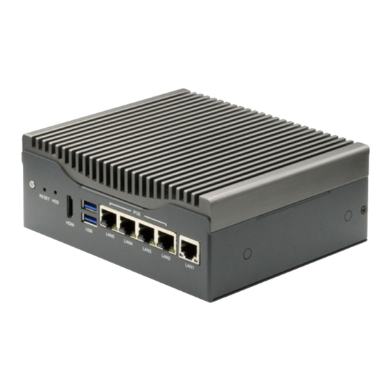
1 .1 Spe cifications System F o rm Factor Mobile NVR P rocessor Intel® Apollo Lake Processor: Intel® Atom™ x5 E3940 (Default) Intel® Pentium® N4200 (Per Project Basis) Intel® Celeron® N3350 (Per Project Basis) Intel® Atom™ x7 E3950 (w/ Custom Chassis) Chip set —... - Page 16 System HDMI x 1 F ront I/O Panel CanBus connector x 1 (in-vehicle config, optional) RS-232 x 3 (in-vehicle config., optional) R ear I/O Panel DC-In power x 1 8-bit DIO x 1, 4-ch digital input, 4-ch digital output RS-232/422/485 x 2 DP x 1 Audio Line-out x 1 Mic-In x 1...
- Page 17 Powe r Requirement Po wer Supply DC 12-24V DC 9-36V with power ignition (in-vehicle config., optional) Me chanical R emovable HDD Tray — I nt ernal System HDD Bay — Dimension 160mm (L) x 134mm (W) x 62mm (H) Gross Weight 1.8 kg N o te —...
-
Page 18: Chapter 2 - Hardware Information
Chapter 2 Chapter 2 – Hardware Information... -
Page 19: Dimensions
Di mensions The VPC-3350S is available in two configurations, Industrial and In-vehicle. Y ou may refer to this section for either configuration. If you have questions about your VPC-3350S or its configuration, please contact your AAEON sales representative. 2.1 .1 Industrial System Chapter 2 –... - Page 20 Chapter 2 – Hardware Information...
- Page 21 Chapter 2 – Hardware Information...
-
Page 22: In-Vehicle System
2.1 .2 In-Vehicle System Chapter 2 – Hardware Information... - Page 23 Chapter 2 – Hardware Information...
-
Page 24: Main Board
2.1 .3 Mai n Board Chapter 2 – Hardware Information... -
Page 25: Jumpers And Connectors
2.2 Jum pers and Connectors To p Side Chapter 2 – Hardware Information... - Page 26 B o ttom Side Chapter 2 – Hardware Information...
-
Page 27: List Of Jumpers
2.3 Li st of Jumpers Please refer to the table below for all of the system’s jumpers that you can configure for your application. Lab el F unction CN 13 Clear CMOS 2.3 .1 Cl e ar CMOS (CN13) CN13 Clear CMOS uses a 6-pin configuration. Use two jumpers to connect the pins according to the chart. -
Page 28: List Of Connectors
2.4 Li st of Connectors Please refer to the table below for all of the system’s connectors that you can co nfigure for your application Lab el F unction A U DIO1 Front Out/ Microphone CN 1 Dual USB3.0 CN 2 Ethernet 1 (without PoE) CN 3 HDMI Connector... -
Page 29: Front Panel (Cn4)
Lab el F unction SW 2 Software Reset 2.4.1 Front Panel ( CN4) P in Sig nal P in Sig nal PWR_SW# (For Car PC) FPANSWH# (For Car PC) HW_RST# FPANSWH# 2.4.2 E xpansion Board Connector (CN8) Chapter 2 – Hardware Information... -
Page 30: Vehicle Power Board Expansion Connector (Cn9)
2.4.3 Ve hicle Power Board E xpansion Connector ( CN9) P in Sig nal P in Sig nal PS_ON# PWRBD_EN REMOTE_SW ACC_IN PWR_SW# 2.4.4 SATA Power Connector ( CN14) P in Sig nal P in Sig nal Chapter 2 – Hardware Information... -
Page 31: Digital Io Connector (Cn19)
2.4.5 Di gital IO Connector ( CN19) P in Sig nal P in Sig nal GPIO Port1 GPIO Port5 GPIO Port2 GPIO Port6 GPIO Port3 GPIO Port7 GPIO Port4 GPIO Port8 GP IO Mapping for DIO Connector (CN19) P in Sig nal GP IO Mapping P in... -
Page 32: Dc Input 12~24V (Cn24)
GP IO Spec Table Dig ital IO Spec N o n-Isolation I s olation (Per Project Basis) Vil=0~0.8V Vil=0~1.5V I np ut Level Vih=2.0~5V Vih=3.5~5V Out put Type open drain Push-Pull Lo <0.4V, max 12mA Lo <0.4V, max 4mA Out put Level & Current Hi >2.4V, max 0.5mA Hi >4.6V, max 4mA... -
Page 33: Vehicle Power Board Expansion Connector (Cn39)
2.4.7 Ve hicle Power Board E xpansion Connector ( CN39) P in Sig nal P in Sig nal Ground DCIN Ground DCIN Ground V-out (by PER-T528) Ground V-out (by PER-T528) 2.4.8 Se ri al Port 1 / Port 2 (RS232/422/485) ( COM1) P in Sig nal P in... -
Page 34: Software Reset (Sw2) Gpio Mapping
2.4.9 Sof tware Reset (SW2) GPIO Mapping SW 2 GPIO Mapping Mapping SIO F81866 GP76 Chapter 2 – Hardware Information... -
Page 35: Option Board Dimensions
2.5 Option Board Dimensions The VPC-3350S In-Vehicle configuration comes with two option boards, PER-T528 Power Board, and PER-T529 I/O Board. If you have any questions about the configuration of your VPC-3350S, please contact your AAEON sales representative for assistance. 2.5.1 PE R-T528 Power Board Dimensions Chapter 2 –... -
Page 36: Per-T529 I/O Board Dimensions
2.5.2 PE R-T529 I/O Board Dimensions Chapter 2 – Hardware Information... -
Page 37: Option Board Assembly
2.5.3 Option Board Assembly Chapter 2 – Hardware Information... -
Page 38: Option Board Jumpers And Connectors
2.6 Option Board Jumpers and Connectors The VPC-3350S In-Vehicle configuration comes with two option boards, PER-T528 Power Board, and PER-T529 I/O Board. If you have any questions about the configuration of your VPC-3350S, please contact your AAEON sales representative for assistance. -
Page 39: Per-T528 List Of Connectors
2.6.3 PE R-T528 List of Connectors Lab el F unction CN 1 DC-Input CN 2 Fuse Slot CN 3 12VSB Output CN 5 MCU Program Header CN 9 Board-To-Board Cable Connector 2.6.3.1 DC-Input ( CN1) P in Sig nal P in Sig nal 2.6.3.2 1 2VSB Output (CN3) -
Page 40: Board To Board Cable Connector (Cn9)
2.6.3.3 Board to Board Cable Connector (CN9) P in Sig nal P in Sig nal UART RX Remote_SW# PS_ON# Ignition_SW UART TX Power Button# None Chapter 2 – Hardware Information... -
Page 41: Per-T529 I/O Board Jumpers And Connectors
2.6.4 PE R-T529 I/O Board Jumpers and Connectors To p B o ttom Chapter 2 – Hardware Information... -
Page 42: Per-T529 List Of Jumpers
2.6.5 PE R-T529 List of Jumpers Lab el F unction CN 6 RSVD for Debug CN 7 RSVD for Debug 2.6.5.1 CAN Bus MCU Debug (CN6) P in Selection F unction 1- 2 Normal (Default) 2- 3 Debug 2.6.5.2 CAN Bus MCU Debug (CN7) P in Selection F unction 1- 2... -
Page 43: Per-T529 List Of Connectors
2.6.6 PE R-T529 List of Connectors Lab el F unction CN 1 COM Port (RS232 only) CN 2 COM Port (RS232 only) CN 3 COM Port (RS232 only) CN 4 CAN Bus Connector CN 5 GPS Antenna Connector CN 8 Board to Board Connector CN 9 Mini Card Slot (Full Function) with SIM3... -
Page 44: Board To Board Connector (Cn8)
2.6.6.2 Board to Board Connector (CN8) 2.6.6.3 Powe r Input Connector (CN12) P in Sig nal P in Sig nal Ground PWR IN Ground PWR IN Chapter 2 – Hardware Information... -
Page 45: Hdd/Ssd 2.5" Drive Installation
2.7 HDD/SSD 2.5” Drive Installation This section details the steps to install or remove the 2.5” hard drive or solid state drive (SSD). Before beginning these steps, please ensure the VPC-3350S system is shut down (not in sleep or suspended mode) and the power supply is disconnected. St ep 1 Remove the wall mount brackets. - Page 46 St ep 2 Remove the screws securing the bottom cover. First the side screws, then the COM port fasteners. Chapter 2 – Hardware Information...
- Page 47 St ep 3 Remove the bottom cover by sliding the cover toward the rear. St ep 4 Remove the HDD/SSD assembly by removing the screws located on the bottom of the cover. Y ou can now remove the old drive and/or install a new one. Chapter 2 –...
-
Page 48: Sim Card Installation
2.8 SIM Card Installation Refer to the following pictures for how to insert the SIM cards into the SIM slot. To avoid damage to the system or unwanted operation, do not attempt to insert the cards in any other configuration than what is shown. SIM1: Exposed card side down, notch is facing to the right. -
Page 49: Chapter 3 - Ami Bios Setup
Chapter 3 Chapter 3 - AMI BIOS Setup... -
Page 50: System Test And Initialization
System Test and Initialization The system uses certain routines to perform testing and initialization during the boot up sequence. If an error, fatal or non-fatal, is encountered, the system will output a few short beeps or display an error message. The system can usually continue the boot up sequence with non-fatal errors. -
Page 51: Ami Bios Setup
3.2 AMI BIOS Setup The AMI BIOS ROM has a pre-installed Setup program that allows users to modify basic system configurations, which is stored in the battery-backed CMOS RAM and BIOS NVRAM so that the information is retained when the power is turned off. To enter BIOS Setup, power on the system and immediately press... -
Page 52: Setup Submenu: Main
3.3 Se tup Submenu: Main Chapter 3 – AMI BIOS Setup... -
Page 53: Setup Submenu: Advanced
3.4 Se tup Submenu: Advanced Chapter 3 – AMI BIOS Setup... -
Page 54: Advanced: Trusted Computing
3.4.1 Advanced: Trusted Computing Op tions Summary Security Device Disabled Sup port Enabled Optimal Default, Failsafe Enables or Disables BIOS support for security device. O.S. will not show Security Device. TCG EFI protocol and INT1A interface will not be available. SHA-1 PCR Bank Disabled Enabled... - Page 55 Op tions Summary P latform Hierarchy Disabled Enabled Optimal Default, Failsafe Enable or Disable Platform Hierarchy St orage Hierarchy Disabled Enabled Optimal Default, Failsafe Enable or Disable Storage Hierarchy End orsement Disabled Hierarchy Enabled Optimal Default, Failsafe Enable or Disable Endorsement Hierarchy TP M2.0 UEFI Spec TCG_1_2 Version...
-
Page 56: Advanced: Cpu Configuration
3.4.2 Advanced: CPU Configuration Op tions Summary A ctive Processor Cores All Optimal Default, Failsafe Number of cores to enable in each processor package. Hyp er-Threading Disabled Enabled Optimal Default, Failsafe Enabled for Windows XP and Linux (OS optimized for Hyper-Threading Technology) and Disabled for other OS (OS not optimized for Hyper-Threading Technology). -
Page 57: Advanced: Sata Drives
3.4.3 Advanced: SATA Drives Op tions Summary Chip set SATA Disabled Enabled Optimal Default, Failsafe Enables or Disables the Chipset SATA Controller. The Chipset SATA controller supports the 2 black internal SATA ports (up to 3Gb/s supported per port). Chapter 3 – AMI BIOS Setup... -
Page 58: Advanced: Usb Configuration
3.4.4 Advanced: USB Configuration Op tions Summary Leg acy USB Support Disabled Enabled Optimal Default, Failsafe Enables Legacy USB support. AUTO option disables legacy support if no USB devices are connected. DISABLE option will keep USB devices available only for EFI applications. -
Page 59: Advanced: Sdio Configuration
3.4.5 Advanced: SDIO Configuration Op tions Summary Mass Storage Devices: Auto Optimal Default, Failsafe Floppy Forced FDD Hard Disk Mass storage device emulation type. 'AUTO' enumerates devices less than 530MB as floppies. Forced FDD option can be used to force HDD formatted drive to boot as FDD. -
Page 60: Advanced: Hardware Monitor
3.4.6 Advanced: Hardware Monitor Chapter 3 – AMI BIOS Setup... -
Page 61: Advanced: Sio Configuration
3.4.7 Advanced: SIO Configuration Chapter 3 – AMI BIOS Setup... -
Page 62: Serial Port 1 Configuration
3.4.7.1 Se ri al Port 1 Configuration Op tions Summary U s e This Device Disabled Enabled Optimal Default, Failsafe Enable or Disable this Logical Device. Po ssible: Use Automatic Settings Optimal Default, Failsafe IO=2F8h; IRQ=3; IO=3F8h; IRQ=4; Allows user to change Device's Resource settings. New settings will be reflected on This Setup Page after System restarts. -
Page 63: Serial Port 2 Configuration
3.4.7.2 Se ri al Port 2 Configuration Op tions Summary U s e This Device Disabled Enabled Optimal Default, Failsafe Enable or Disable this Logical Device. Po ssible: Use Automatic Settings Optimal Default, Failsafe IO=2F8h; IRQ=3; IO=3F8h; IRQ=4; Allows user to change Device's Resource settings. New settings will be reflected on This Setup Page after System restarts. -
Page 64: Advanced: Power Management
3.4.8 Advanced: Power Management Op tions Summary Po wer Mode ATX Type Optimal Default, Failsafe AT Type Select Power Supply Mode. R estore AC Power Loss Power Off Power On Last State Optimal Default, Failsafe Select AC power state when power is re-applied after a power failure. R TC wake system from Disabled Optimal Default, Failsafe... -
Page 65: Advanced: Digital Io Port Configuration
3.4.9 Advanced: Digital IO Port Configuration Op tions Summary DI O Port5~8 Output Optimal Default, Failsafe Input Set DIO as Input or Output. Out put Level High Optimal Default, Failsafe Set output level when DIO pin is output. Chapter 3 – AMI BIOS Setup... -
Page 66: Setup Submenu: Chipset
3.5 Se tup submenu: Chipset Chapter 3 – AMI BIOS Setup... -
Page 67: Chipset: North Bridge
3.5.1 Chi pset: North Bridge Op tions Summary P rimary Display Optimal Default, Failsafe PCIE Select which of IGD/PCI Graphics device should be Primary Display Chapter 3 – AMI BIOS Setup... -
Page 68: Chi Pset: Scc Configuration
3.5.2 Chi pset: SCC Configuration Op tions Summary SCC eMMC Support Disabled (D28:F0) Enabled Optimal Default, Failsafe Enable/Disable SCC eMMC Support eMMC Max Speed HS400 Optimal Default, Failsafe HS200 DDR50 Select the eMMC max Speed allowed. Chapter 3 – AMI BIOS Setup... -
Page 69: Setup Submenu: Security
3.6 Se tup submenu: Security Change User/Administrator Password Y ou can set an Administrator Password or User Password. An Administrator Password must be set before you can set a User Password. The password will be required during boot up, or when the user enters the Setup utility. A User Password does not provide access to many of the features in the Setup utility. -
Page 70: Security: Secure Boot
3.6.1 Se curity: Secure Boot Op tions Summary Secure Boot Disabled Optimal Default, Failsafe Enabled Secure Boot activated when Secure Boot is enabled, Platform Key(PK) is enrolled, System mode is User/Deployed, and CSM is disabled Secure Boot Custom Optimal Default, Failsafe Cus tomization Standard Customizable Secure Boot mode:... -
Page 71: Key Management
3.6.1.1 Ke y Management Op tions Summary Factory Key Provision Disabled Optimal Default, Failsafe Enabled Provision factory default keys on next re-boot only when System in Setup Mode R estore Factory Keys Y es Optimal Default, Failsafe Force System to User Mode. Configure NVRAM to contain OEM-defined factory default Secure Boot keys R eset To Setup Mode Y es... - Page 72 Op tions Summary Enroll Efi Image Optimal Default, Failsafe Copy NVRAM content of Secure Boot variables to files in a root folder on a file system device R emove 'UEFI CA' from Y es Optimal Default, Failsafe Device Guard ready system must not list 'Microsoft UEFI CA' Certificate in Authorized Signature database (db) R estore DB defaults Y es...
-
Page 73: Setup Submenu: Boot
3.7 Se tup submenu: Boot Op tions Summary Quiet Boot Disabled Enabled Optimal Default, Failsafe Enables or disables Quiet Boot option. CSM Support Disabled Enabled Optimal Default, Failsafe Enable/Disable CSM Support Launch PXE ROM Disabled Optimal Default, Failsafe Enabled Controls the execution of UEFI and Legacy PXE OpROM N etwork Stack Disabled Optimal Default, Failsafe... -
Page 74: Setup Submenu: Save & Exit
3.8 Se tup submenu: Save & Exit Chapter 3 – AMI BIOS Setup... -
Page 75: Chapter 4 - Driver And Software Installation
Chapter 4 Chapter 4 – Driver and Software Installation... -
Page 76: Drivers Download And Installation
Dri vers Download and Installation Drivers for the VPC-3350S can be downloaded from the product page on the AAEON website. Download the driver(s) you need and follow the steps below to install them . St ep 1 – Install Chipset Driver Open the St ep1 - Chipset folder followed by SetupChipset.exe Follow the instructions Drivers will be installed automatically... - Page 77 St ep 5 – Install LAN Driver Open the St ep5 - LAN folder and select your OS Open the Set up.exe file in the folder Follow the instructions Drivers will be installed automatically St ep 6 – Install Serial Port Driver (optional) Open the St ep6 –...
-
Page 78: Appendix A - Watchdog Timer Programming
Appendix A Appendix A - Watchdog Timer Programming... -
Page 79: Watchdog Timer Initial Program
Watchdog T imer Initial Program Tab le 1 : SuperIO relative register table Default Value N o te SIO MB PnP Mode Index Register Index 0x2E(Note1) 0x2E or 0x4E SIO MB PnP Mode Data Register Dat a 0x2F(Note2) 0x2F or 0x4F Tab le 2 : Watchdog relative register table R egister B itNum... - Page 80 ************************************************************************************ // SuperIO relative definition (Please reference to Table 1) #d efine byte SIOIndex //This parameter is represented from N o te1 #d efine byte SIOData //This parameter is represented from N o te2 #d efine vo id IOWriteByte(b yte IOPort, b yte Value); #d efine b yte IOReadByte(b yte IOPort);...
- Page 81 ************************************************************************************ VOID Main(){ // Procedure : AaeonWDTConfig // (byte)Timer : Time of WDT timer.(0x00~0xFF) // (boolean)Unit : Select time unit(0: second, 1: minute). AaeonWDTConfig(); // Procedure : AaeonWDTEnable // This procudure will enable the WDT counting. AaeonWDTEnable(); ************************************************************************************ Appendix A – Watchdog Timer Programming...
- Page 82 ************************************************************************************ // Procedure : AaeonWDTEnable VOID A aeonWDTEnable (){ WDTEnableDisable(Enab leLDN, EnableReg, EnableBit, 1); // Procedure : AaeonWDTConfig VOID A aeonWDTConfig (){ // Disable WDT counting WDTEnableDisable(Enab leLDN, EnableReg, EnableBit, 0); // Clear Watchdog Timeout Status WDTClearTimeoutStatus(); // WDT relative parameter setting WDTParameterSetting();...
- Page 83 ************************************************************************************ VOID SI OEnterMBPnPMode(){ IOWriteByte(SIOIndex, 0x87); IOWriteByte(SIOIndex, 0x87); VOID SI OExitMBPnPMode(){ IOWriteByte(SIOIndex, 0xAA); VOID SI OSelectLDN(byte LDN){ IOWriteByte(SIOIndex, 0x07); // SIO LDN Register Offset = 0x07 IOWriteByte(SIOData, LDN); VOID SI OBitSet(byte LDN, byte Register, byte BitNum, byte Value){ Byte TmpValue; SIOEnterMBPnPMode();...
-
Page 84: Appendix B - Digital I/O Ports
Appendix B Appendix B – Digital I/O Ports... -
Page 85: Electrical Specifications For Dig Ital I/O Ports
E l ectrical Specifications for Digital I/O Ports GPIO80 ISOGPI0 Input Only GPIO81 ISOGPI1 Input Only GPIO82 ISOGPI2 Input Only GPIO83 ISOGPI3 Input Only GPIO84 ISOGPO0 Output Only GPIO85 ISOGPO1 Output Only GPIO86 ISOGPO2 Output Only GPIO87 ISOGPO3 Output Only Appendix B –... -
Page 86: Dio Programming
B.2 DIO Programming The VPC-3350S utilizes FINTEK F81866D chipset as its Digital I/O controller. Below are the procedures to complete its configuration. AAEON initial DI/O program is also attached for developing customized program for your application. There are three steps to complete the configuration setup: (1) Enter the MB PnP Mode (2) Modify the data of configuration registers (3) Exit the MB PnP Mode. -
Page 87: Digital I/O Register
B.3 Di gital I/O Register Tab le 1 : SuperIO relative register table Default Value N o te SIO MB PnP Mode Index Register Index 0x2E(Note1) 0x2E or 0x4E SIO MB PnP Mode Data Register Dat a 0x2F(Note2) 0x2F or 0x4F Tab le 2 : Digital Input relative register table R egister B itNum... -
Page 88: Digital I/O Sample Program
B.4 Di gital I/O Sample Program ************************************************************************************ // SuperIO relative definition (Please reference to Table 1) #d efine byte SIOIndex //This parameter is represented from N o te1 #d efine byte SIOData //This parameter is represented from N o te2 #d efine vo id IOWriteByte(b yte IOPort, b yte Value);... - Page 89 ************************************************************************************ // Digital Output control relative definition (Please reference to Table 3) #d efine byte DOutput1LDN // This parameter is represented from N ote27 #d efine byte DOutput1Reg // This parameter is represented from N o te28 #d efine byte DOutput1Bit // This parameter is represented from N o te29 #d efine byte DOutput1Val // This parameter is represented from N o te30 #d efine byte DOutput2LDN // This parameter is represented from N ote31 #d efine byte DOutput2Reg // This parameter is represented from N o te32...
- Page 90 ************************************************************************************ VOID Main(){ Boolean PinStatus ; // Procedure : AaeonReadPinStatus // Input : Example, Read Digital I/O Pin 3 status // Output : InputStatus : 0: Digital I/O Pin level is low 1: Digital I/O Pin level is High PinStatus = AaeonReadPinStatus(DI nput3LDN, DInput3Reg, DInput3Bit); // Procedure : AaeonSetOutputLevel // Input : Example, Set Digital I/O Pin 6 level...
- Page 91 ************************************************************************************ Boolean A aeonReadPinStatus(byte LDN, byte Register, byte BitNum){ Boolean PinStatus ; PinStatus = SIOBitRead(LDN, Register, BitNum); Return PinStatus ; VOID A aeonSetOutputLevel(byte LDN, byte Register, byte BitNum, byte Value){ ConfigToOutputMode(LDN, Register, BitNum); SIOBitSet(LDN, Register, BitNum, Value); ************************************************************************************ Appendix B – Digital I/O Ports...
- Page 92 ************************************************************************************ VOID SI OEnterMBPnPMode(){ IOWriteByte(SIOIndex, 0x87); IOWriteByte(SIOIndex, 0x87); VOID SI OExitMBPnPMode(){ IOWriteByte(SIOIndex, 0xAA); VOID SI OSelectLDN(byte LDN){ IOWriteByte(SIOIndex, 0x07); // SIO LDN Register Offset = 0x07 IOWriteByte(SIOData, LDN); VOID SI OBitSet(byte LDN, byte Register, byte BitNum, byte Value){ Byte TmpValue; SIOEnterMBPnPMode();...
- Page 93 ************************************************************************************ Boolean SI OBitRead(byte LDN, byte Register, byte BitNum){ Byte TmpValue; SIOEnterMBPnPMode(); SIOSelectLDN(LDN); IOWriteByte(SIOIndex, Register); TmpValue = IOReadByte(SIOData); TmpValue &= (1 << BitNum); SIOExitMBPnPMode(); If(TmpValue == 0) Return 0; Return 1; VOID Co nfigToOutputMode(byte LDN, byte Register, byte BitNum){ Byte TmpValue, OutputEnableReg; OutputEnableReg = Register-1;...