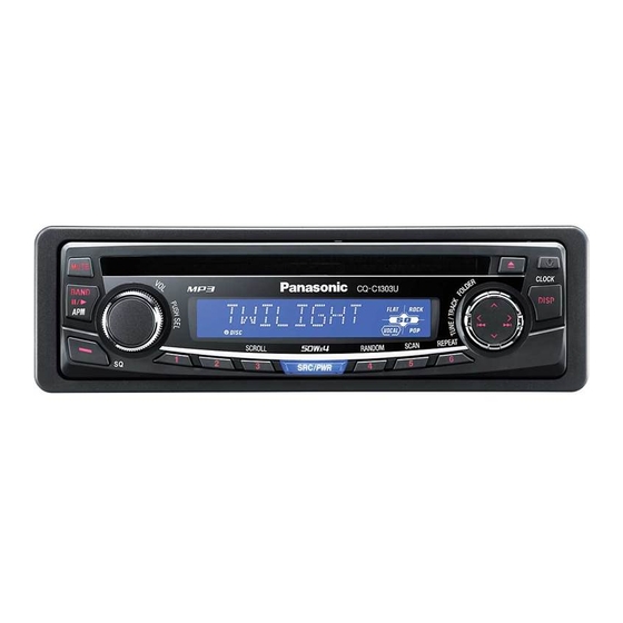
Panasonic CQ-C1303U Service Manual
Removable front panel cd player/receiver
Hide thumbs
Also See for CQ-C1303U:
- Operating instructions manual (21 pages) ,
- Manual de instrucciones (20 pages) ,
- Operating instructions manual (28 pages)
Table of Contents
Quick Links
Specifications*
General
Power Supply
Tone Controls
Current Consumption
Maximum Power Output
Suitable Speaker Impedance
Pre-Amp Output Voltage
Output Impedance
FM Stereo Radio
Frequency Range
Usable Sensitivity
AM Radio
Frequency Range
DC 12V (11V - 16V),
Test Voltage 14.4V
Negative Ground
Bass ; ±12dB at 100Hz
Treble ; ±12dB at 10kHz
Less than 2.2A (CD play mode,
0.5W×4ch)
50W×4ch (at 1kHz, Vol. Max.)
4-8Ω
2.5V (CD play mode; 1kHz, 0dB)
200Ω
87.9 - 107.9MHz
11.0dBf (1.25µV, 75Ω)
530 - 1,710kHz
AUTOMOTIVE AFTERMARKET
CQ-C1303U
Removable Front Panel CD Player /
Receiver
Usable Sensitivity
CD Player
Sampling Frequency
Pick-Up Type
Light Source
Wavelength
Frequency Response
Signal to Noise Ratio
Dimensions**
Weight**
* Specifications and the design are subject to possible modification
without notice due to improvements.
** Dimensions and Weight shown are approximate.
© 2005 Matsushita Electric Industrial Co., Ltd. All
rights
reserved.
distribution is a violation of law.
Order No. ACED051213C7
28dB/µV (25µV, S/N 20dB)
8 times oversampling
Astigma 3-beam
Semiconductor Laser
780nm
20Hz to 20,000Hz (±1dB)
96dB
178×50×155mm
1.4kg
Unauthorized
copying
and
C4
Table of Contents

Related Manuals for Panasonic CQ-C1303U


Summary of Contents for Panasonic CQ-C1303U
- Page 1 Order No. ACED051213C7 AUTOMOTIVE AFTERMARKET CQ-C1303U Removable Front Panel CD Player / Receiver Specifications* General Usable Sensitivity 28dB/µV (25µV, S/N 20dB) Power Supply DC 12V (11V - 16V), Test Voltage 14.4V Negative Ground CD Player Tone Controls Bass ; ±12dB at 100Hz...
-
Page 2: Table Of Contents
CQ-C1303U CONTENTS Page Page 1 ABOUT LEAD FREE SOLDER (PbF) 11 PACKAGE AND IC BLOCK DIAGRAM 2 FEATUERS 12 REPLACEMENT PARTS LIST 3 LASER PRODUCTS 13 EXPLODED VIEW (Unit) 4 REPLACEING THE FUSE 14 CD PLAYER MECHANICAL PARTS LIST 5 MAINTENANCE... -
Page 3: Maintenance
CQ-C1303U 5 MAINTENANCE Your products is designed and manufactured to ensure a minimum of maintenance. Use a dry, a soft cloth for routine exterior cleaning. Never use benzine, thinner or other solvents. 6 NOTES [RADIO BLOCK] Do not align the AM/FM package block. When the package block is necessary, it will be supplied already aligned at the factory. -
Page 4: Wiring Connection
CQ-C1303U 8 WIRING CONNECTION... -
Page 5: Block Diagram
CQ-C1303U 9 BLOCK DIAGRAM... -
Page 6: Terminals Description
CQ-C1303U 10 TERMINALS DESCRIPTION 10.1. Main Block IC601 : LC7237819D09 Part No. Part Name & I/O(V) FM( AM(V CD(V Description Part No. Part Name & I/O(V) FM( AM(V CD(V Description 51 AMP_MUTE Amp mute 5.19 5.19 X’tal 2.54 2.53 52 N.C. - Page 7 CQ-C1303U Part No. Part Name & I/O(V) FM( AM(V CD(V Ref. Part No. Part Name & Description Description DVDD18 VDD capacitor connection port 1.83 for digital circuit. 98 EO1 phase comparison 2.02 0 MONI0 Monitor port0. error output MONI1 Monitor port1.
- Page 8 CQ-C1303U 10.2. Display Block IC901 : YEAMLC75854W Pin No. Port Descriptions No connection 5-39 SEG5-39 LCD segment 40-43 COM1-4 LCD common 44-49 KS1-6 Key data output 50-54 KI1-5 Key data input TEST (Connecting to ground) +5V power supply VDD1 Ground through capacitor...
-
Page 9: Package And Ic Block Diagram
CQ-C1303U 11 PACKAGE AND IC BLOCK DIAGRAM 11.1. Main Block PA51:J3CCBB000005 IC271 : C1EA00000041... - Page 10 CQ-C1303U IC401 : C1BB00001088 IC701 : C0DAZHF00004...
- Page 11 CQ-C1303U IC251 : C1BB00000804...
-
Page 12: Replacement Parts List
CQ-C1303U 12 REPLACEMENT PARTS LIST Ref. Part No. Part Name & Description Remarks DISPLAY BLOCK [E-4C287] D901 YEADSPADB01 LED (BLUE) D902 YEADSPADR01 LED (RED) D903 YEADSPADR01 LED (RED) D905 YEADSPADR01 LED (RED) D906 YEADSPADR01 LED (RED) D907 YEADSPADR01 LED (RED) - Page 13 CQ-C1303U Ref. Part No. Part Name & Description Remarks Ref. Part No. Part Name & Description Remarks C450 F2A0J101A020 Electrolytic 100pF 6.3WV C904 F1J1H681A733 Ceramic 680pF 50WV C451 F2A0J101A049 Electrolytic 100pF 6.3WV C907 F1J1H103A733 Ceramic 0.01MFD 50WV C471 F1J1H104A036 Ceramic 0.1MFD 50WV...
- Page 14 CQ-C1303U Ref. Part No. Part Name & Description Remarks Ref. Part No. Part Name & Description Remarks ERJ8GX0R00V Chip 0 ohms 1/8W R602 D0GD473JA017 Chip 47k ohms 1/10W ERJ8GX0R00V Chip 0 ohms 1/8W R605 D0GF473JA017 Chip 47k ohms 1/10W ERJ8GX0R00V...
- Page 15 CQ-C1303U Ref. Part No. Part Name & Description Remarks Ref. Part No. Part Name & Description Remarks ERJ8GX0R00V Chip 0 ohms 1/8W YFM284C484CA Operating Instructions(ENGLISH) ERJ8GX0R00V Chip 0 ohms 1/8W YFM284C485CA Operating ERJ8GX0R00V Chip 0 ohms 1/8W Instructions(FRANCE) ERJ8GX0R00V Chip 0 ohms 1/8W...
-
Page 16: Exploded View (Unit)
CQ-C1303U 13 EXPLODED VIEW (Unit) -
Page 17: Cd Player Mechanical Parts List
CQ-C1303U 14 CD PLAYER MECHANICAL PARTS LIST Ref. Part No. Part Name & Description Remarks 3032 10 40 SW WIRE MN N(A-1) 3032 10 39 SP WIRE MN N(D-2) 3032 10 13 WIRE CLAMPER M N(C-2); N(C-3); N(D-4); N(E-3) 3032 10 28... -
Page 18: Exploded View (Cd Deck)
CQ-C1303U 15 EXPLODED VIEW (CD Deck) -
Page 19: Packing Parts List
CQ-C1303U 16 PACKING PARTS LIST .Item numbers listed below should not order reguler spare parts. (not available) Item No. Part No. Part Name & Description Q’ty Remarks Inner Carton Not available Packing Pad Front Not available Packing Pad Rear Not available... -
Page 20: Wiring Diagram
CQ-C1303U 17 WIRING DIAGRAM 17.1. Main Block-1 [E-4C286][TOP VIEW] CQ-C1303H/C1303U/C1301NE/C1303NW/C1313NE/C1313NW CQ-C1323NE/C1323NW/C1333U/C1333W MAIN PCB... - Page 21 CQ-C1303U 17.2. Main Block-2 [E-4C286][BOTTOM VIEW] CQ-C1303H/C1303U/C1301NE/C1303NW/C1313NE/C1313NW CQ-C1323NE/C1323NW/C1333U/C1333W MAIN PCB...
- Page 22 CQ-C1303U 17.3. Display Block [E-4C287][TOP VIEW] [E-4C287][BOTTOM VIEW] CQ-C1313NE/C1313NW/C1323NE/C1323NW/C1333U/C1333W CQ-C1303H/C1303U/C1303NE/C1303NW DISPLAY PCB...
- Page 23 CQ-C1303U 17.4. CD Interface Block [E-4C288][BOTTOM VIEW] CQ-C1103U/W/H/D CQ-C1333U/W CQ-C1303U/W/H/D/NE/NW CQ-C1313NE/NW CQ-C1323NE/NW CD INTERFACE PCB...
- Page 24 THIS PAGE IS JUST FOR THE PAGE LAYOUT USE ONLY.
-
Page 25: Schematic Diagram-1
CQ-C1303U 18 SCHEMATIC DIAGRAM-1 18.1. Main Block E-4C286 0.12 0.26 0.36 13.06 12.36 0.13 5.12 4.57 4.52 5.23 4.57 4.53 4.57 5.21 4.57 4.52 4.53 0.68 4.52 4.53 4.56 5.17 4.53 5.17 4.55 5.21 5.23 0.89 8.22 8.21 8.11 8.22 8.16... - Page 26 THIS PAGE IS JUST FOR THE PAGE LAYOUT USE ONLY.
-
Page 27: Schematic Diagram-2
CQ-C1303U 19 SCHEMATIC DIAGRAM-2 19.1. Display Block... - Page 28 CQ-C1303U 19.2. CD Interface Block...
-
Page 29: Schematic Diagram For Printing With A4 Size
CQ-C1303U 20 SCHEMATIC DIAGRAM for printing with A4 size 20.1. Main Block (Left Side) 0.12 0.26 0.36 4.57 4.52 5.23 4.57 4.53 4.57 5.21 4.52 4.57 4.53 0.68 4.52 4.53 4.56 5.17 4.53 5.17 4.55 8.22 8.21 8.11 8.22 8.16 8.18... - Page 30 CQ-C1303U 20.2. Main Block (Right Side) E-4C286 13.06 12.36 0.13 5.12 4.57 4.52 4.57 4.53 4.57 4.52 4.57 4.53 0.68 4.52 4.53 4.56 5.17 4.53 5.17 4.55 5.21 5.23 0.89 3.25 3.25 1.08 1.83 0.08 3.29 1.23 1.84 1.04 1.65 0.88...