Table of Contents
Quick Links
www.ti.com
User's Guide
TPS53313 Step-Down Converter Evaluation Module User's
Guide
1
Introduction.............................................................................................................................................................................3
2 Description..............................................................................................................................................................................
Applications............................................................................................................................................................3
2.2 Features.............................................................................................................................................................................
3 Electrical Performance Specifications.................................................................................................................................
4
Schematic................................................................................................................................................................................4
Setup................................................................................................................................................................................5
5.1 Test Equipment..................................................................................................................................................................
Setup.................................................................................................................................................6
6 Configurations........................................................................................................................................................................
6.1 Mode and Soft-Start Time Selection..................................................................................................................................
6.2 Overcurrent Protection (OCP) Selection............................................................................................................................
6.3 Enable Selection................................................................................................................................................................
7 Test Procedure........................................................................................................................................................................
7.1 Line/Load Regulation and Efficiency Measurement Procedure.........................................................................................
7.2 Control Loop Gain and Phase Measurement Procedure...................................................................................................
7.3 List of Test Points...............................................................................................................................................................
7.4 Equipment Shutdown.........................................................................................................................................................
8 Performance Data and Typical Characteristic Curves........................................................................................................
8.1
Efficiency............................................................................................................................................................................9
8.2 Load Regulation.................................................................................................................................................................
8.3 Line Regulation................................................................................................................................................................
Transient...............................................................................................................................................................11
8.5 Output Ripple...................................................................................................................................................................
8.6 Switching Node................................................................................................................................................................
8.7 Start Up............................................................................................................................................................................
Down........................................................................................................................................................................15
8.9 Over-Current Protection...................................................................................................................................................
8.10
Synchronization..............................................................................................................................................................16
Plot........................................................................................................................................................................16
8.12 Thermal Image...............................................................................................................................................................
9 EVM Assembly Drawing and PCB Layout..........................................................................................................................
10 List of Materials..................................................................................................................................................................
History..................................................................................................................................................................22
Figure 5-2. TPS53313EVM-078 Recommended Test Set Up.....................................................................................................
Figure 8-1. Efficiency...................................................................................................................................................................
Figure 8-2. Load Regulation........................................................................................................................................................
Figure 8-3. Line Regulation.......................................................................................................................................................
Figure 8-4. Output Load 0-A to 3-A Transient Under FCCM Mode (12-V VIN, 1.2-V VOUT, f
Figure 8-6. Output Ripple at No Load (12-V VIN, 1.2-V VOUT, 0-A, Skip Mode, f
Figure 8-7. Output Ripple at Full Load (12-V VIN, 1.2-V VOUT, 6-A, Skip Mode, f
Figure 8-8. Switching Node at No Load (12-V VIN, 1.0-V VOUT, 0-A, Skip Mode, f
Figure 8-9. Switching Node at Full Load (12-V VIN, 1.2-V VOUT, 6-A, Skip Mode, f
SLUU819A - DECEMBER 2011 - REVISED DECEMBER 2021
Submit Document Feedback
Table of Contents
List of Figures
Schematic.................................................................................................................................4
Ripple..........................................................................................................5
Copyright © 2021 Texas Instruments Incorporated
Synchronization.....................................................................7
SW
= 600 kHz)...............................
= 600 kHz).............................................
SW
= 600 kHz)............................................
SW
= 600 kHz)..........................................
SW
= 600 kHz).........................................
SW
TPS53313 Step-Down Converter Evaluation Module User's Guide
Table of Contents
= 600
kHz)............................11
3
3
3
5
7
7
7
7
8
8
8
8
8
9
9
10
12
13
14
15
17
18
21
6
9
9
10
11
12
12
13
13
1
Table of Contents

Related Manuals for Texas Instruments TPS53313EVM-078


Summary of Contents for Texas Instruments TPS53313EVM-078
-
Page 1: Table Of Contents
Figure 4-1. TPS53313EVM-078 Schematic..........................4 Figure 5-1. Tip and Barrel Measurement for VOUT Ripple......................5 Figure 5-2. TPS53313EVM-078 Recommended Test Set Up..................... Figure 8-1. Efficiency................................... Figure 8-2. Load Regulation................................ Figure 8-3. Line Regulation............................... Figure 8-4. Output Load 0-A to 3-A Transient Under FCCM Mode (12-V VIN, 1.2-V VOUT, f = 600 kHz)......11... - Page 2 = 600 kHz)..........Figure 8-17. Thermal Image (12-V VIN, 1.2-V VOUT, 6-A IOUT, FCCM Mode, f = 1.00 MHz)..........Figure 9-1. TPS53313EVM-078 Top Layer Assembly Drawing (top view)................Figure 9-2. TPS53313EVM-078 Bottom Assembly Drawing (bottom view)................18 Figure 9-3. TPS53313EVM-078 Top Copper (top view)......................
-
Page 3: Introduction
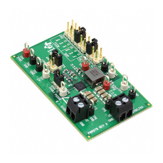
TPS53313 is a fully integrated step-down regulator employing voltage mode control. 2 Description The TPS53313EVM-078 is designed to use a 12-V voltage rail to produce a regulated 1.2-V output with up to 6-A load current. The TPS53313EVM-078 is designed to demonstrate the TPS53313 in a typical Point-Of-Load (POL) application while providing a number of test points to evaluate the performance of the TPS53313. -
Page 4: Schematic
Schematic www.ti.com 4 Schematic Figure 4-1. TPS53313EVM-078 Schematic TPS53313 Step-Down Converter Evaluation Module User's Guide SLUU819A – DECEMBER 2011 – REVISED DECEMBER 2021 Submit Document Feedback Copyright © 2021 Texas Instruments Incorporated... -
Page 5: Test Setup
J5 to LOAD: The minimum recommended wire size is 1x AWG #16, with the total length of wire less than 4 feet (2 feet output, 2 feet return). SLUU819A – DECEMBER 2011 – REVISED DECEMBER 2021 TPS53313 Step-Down Converter Evaluation Module User's Guide Submit Document Feedback Copyright © 2021 Texas Instruments Incorporated... -
Page 6: Recommended Test Setup
5.2 Recommended Test Setup Figure 5-2 is the recommended test set up to evaluate the TPS53313EVM-078. Working at an ESD workstation, make sure that any wrist straps, bootstraps or mats are connected referencing the user to earth ground before power is applied to the EVM. -
Page 7: Configurations
Table 6-3. Switching Frequency Selection SWITCHING FREQUENCY SETTING RESISTANCES SWITCHING FREQUENCY 80.6 kΩ 600 kHz 45.3 kΩ 1.00 MHz SLUU819A – DECEMBER 2011 – REVISED DECEMBER 2021 TPS53313 Step-Down Converter Evaluation Module User's Guide Submit Document Feedback Copyright © 2021 Texas Instruments Incorporated... -
Page 8: Test Procedure
10. Decrease load to 0 A. 11. Decrease VIN to 0 V. 7.2 Control Loop Gain and Phase Measurement Procedure TPS53313EVM-078 contains a 10-Ω series resistor in the feedback loop for loop response analysis. 1. Set up EVM as described in Section 5 Figure 5-2. -
Page 9: Performance Data And Typical Characteristic Curves
8 Performance Data and Typical Characteristic Curves Figure 8-1 through Figure 8-17 present typical performance curves for TPS53313EVM-078. 8.1 Efficiency VIN = 12 V, fsw = 600 kHz, Skip Mode VIN = 12 V, fsw = 1.00 MHz, Skip Mode VIN = 12 V, fsw = 600 kHz, FCCM Mode VIN = 12 V, fsw = 1.00 MHz, FCCM Mode... -
Page 10: Line Regulation
FCCM Mode, fsw = 1.00 MHz, IOUT = 6 A 1.205 1.195 1.19 1.185 1.18 - Input Voltage - V Figure 8-3. Line Regulation TPS53313 Step-Down Converter Evaluation Module User's Guide SLUU819A – DECEMBER 2011 – REVISED DECEMBER 2021 Submit Document Feedback Copyright © 2021 Texas Instruments Incorporated... -
Page 11: Output Transient
Figure 8-5. Output Load 0-A to 3-A Transient Under Skip Mode (12-V VIN, 1.2-V VOUT, f = 600 kHz) SLUU819A – DECEMBER 2011 – REVISED DECEMBER 2021 TPS53313 Step-Down Converter Evaluation Module User's Guide Submit Document Feedback Copyright © 2021 Texas Instruments Incorporated... -
Page 12: Output Ripple
Figure 8-7. Output Ripple at Full Load (12-V VIN, 1.2-V VOUT, 6-A, Skip Mode, f = 600 kHz) TPS53313 Step-Down Converter Evaluation Module User's Guide SLUU819A – DECEMBER 2011 – REVISED DECEMBER 2021 Submit Document Feedback Copyright © 2021 Texas Instruments Incorporated... -
Page 13: Switching Node
Figure 8-9. Switching Node at Full Load (12-V VIN, 1.2-V VOUT, 6-A, Skip Mode, f = 600 kHz) SLUU819A – DECEMBER 2011 – REVISED DECEMBER 2021 TPS53313 Step-Down Converter Evaluation Module User's Guide Submit Document Feedback Copyright © 2021 Texas Instruments Incorporated... -
Page 14: Start Up
Figure 8-10. Start-Up Waveform (12-V VIN, 1.2-V VOUT, 6-A IOUT, 1-ms SS) Figure 8-11. Pre-bias Start-Up Waveform (12-V VIN, 1.2-V VOUT, 0-A IOUT, 1-ms SS) TPS53313 Step-Down Converter Evaluation Module User's Guide SLUU819A – DECEMBER 2011 – REVISED DECEMBER 2021 Submit Document Feedback Copyright © 2021 Texas Instruments Incorporated... -
Page 15: Shut Down
Figure 8-13. Over-Current Protection Waveform ( 12-V VIN, 1.2-V VOUT, IOUT increases from 6 A to 7.8 A) SLUU819A – DECEMBER 2011 – REVISED DECEMBER 2021 TPS53313 Step-Down Converter Evaluation Module User's Guide Submit Document Feedback Copyright © 2021 Texas Instruments Incorporated... -
Page 16: Synchronization
Figure 8-15. Loop Gain (12-V VIN, 1.2-V VOUT, 6-A IOUT, Skip Mode, f = 600 kHz) TPS53313 Step-Down Converter Evaluation Module User's Guide SLUU819A – DECEMBER 2011 – REVISED DECEMBER 2021 Submit Document Feedback Copyright © 2021 Texas Instruments Incorporated... -
Page 17: Thermal Image
Figure 8-17. Thermal Image (12-V VIN, 1.2-V VOUT, 6-A IOUT, FCCM Mode, f = 1.00 MHz) SLUU819A – DECEMBER 2011 – REVISED DECEMBER 2021 TPS53313 Step-Down Converter Evaluation Module User's Guide Submit Document Feedback Copyright © 2021 Texas Instruments Incorporated... -
Page 18: Evm Assembly Drawing And Pcb Layout
(Figure 9-1 through Figure 9-6) show the design of the TPS53313EVM-078 printed circuit board. The EVM has been designed using 4 Layers, 2-oz copper circuit board. Figure 9-1. TPS53313EVM-078 Top Layer Assembly Drawing (top view) Figure 9-2. TPS53313EVM-078 Bottom Assembly Drawing (bottom view) TPS53313 Step-Down Converter Evaluation Module User's Guide SLUU819A –... - Page 19 EVM Assembly Drawing and PCB Layout Figure 9-3. TPS53313EVM-078 Top Copper (top view) Figure 9-4. TPS53313EVM-078 Layer 2 (top view) SLUU819A – DECEMBER 2011 – REVISED DECEMBER 2021 TPS53313 Step-Down Converter Evaluation Module User's Guide Submit Document Feedback Copyright © 2021 Texas Instruments Incorporated...
- Page 20 EVM Assembly Drawing and PCB Layout www.ti.com Figure 9-5. TPS53313EVM-078 Layer 3 (top view) Figure 9-6. TPS53313EVM-078 Bottom Layer (top view) TPS53313 Step-Down Converter Evaluation Module User's Guide SLUU819A – DECEMBER 2011 – REVISED DECEMBER 2021 Submit Document Feedback Copyright © 2021 Texas Instruments Incorporated...
-
Page 21: List Of Materials
List of Materials 10 List of Materials The EVM components list according to the schematic shown in Figure 4-1 Table 10-1. TPS53313EVM-078 List of Materials REF DES DESCRIPTION PART NUMBER C1, C8, C9 Capacitor, ceramic, 16 V, X7R, 10%, 1.0 µF, 0603 C2, C3, C4, C10, C11, Capacitor, ceramic, 25 V, X5R, 10%, 22 µF, 1206... -
Page 22: Revision History
Revision History www.ti.com Table 10-1. TPS53313EVM-078 List of Materials (continued) REF DES DESCRIPTION PART NUMBER Resistor, chip, 1/16 W, 1%, 39.0 kΩ, 0603 Resistor, chip, 1/16 W, 1%, 82.0 kΩ, 0603 Resistor, chip, 1/16 W, 1%, 160 kΩ, 0603 R14, R18 Resistor, chip, 1/16 W, 1%, 0 Ω, 0603... - Page 23 STANDARD TERMS FOR EVALUATION MODULES Delivery: TI delivers TI evaluation boards, kits, or modules, including any accompanying demonstration software, components, and/or documentation which may be provided together or separately (collectively, an “EVM” or “EVMs”) to the User (“User”) in accordance with the terms set forth herein.
- Page 24 www.ti.com Regulatory Notices: 3.1 United States 3.1.1 Notice applicable to EVMs not FCC-Approved: FCC NOTICE: This kit is designed to allow product developers to evaluate electronic components, circuitry, or software associated with the kit to determine whether to incorporate such items in a finished product and software developers to write software applications for use with the end product.
- Page 25 www.ti.com Concernant les EVMs avec antennes détachables Conformément à la réglementation d'Industrie Canada, le présent émetteur radio peut fonctionner avec une antenne d'un type et d'un gain maximal (ou inférieur) approuvé pour l'émetteur par Industrie Canada. Dans le but de réduire les risques de brouillage radioélectrique à...
- Page 26 www.ti.com EVM Use Restrictions and Warnings: 4.1 EVMS ARE NOT FOR USE IN FUNCTIONAL SAFETY AND/OR SAFETY CRITICAL EVALUATIONS, INCLUDING BUT NOT LIMITED TO EVALUATIONS OF LIFE SUPPORT APPLICATIONS. 4.2 User must read and apply the user guide and other available documentation provided by TI regarding the EVM prior to handling or using the EVM, including without limitation any warning or restriction notices.
- Page 27 Notwithstanding the foregoing, any judgment may be enforced in any United States or foreign court, and TI may seek injunctive relief in any United States or foreign court. Mailing Address: Texas Instruments, Post Office Box 655303, Dallas, Texas 75265 Copyright © 2019, Texas Instruments Incorporated...
- Page 28 TI products. TI’s provision of these resources does not expand or otherwise alter TI’s applicable warranties or warranty disclaimers for TI products. TI objects to and rejects any additional or different terms you may have proposed. IMPORTANT NOTICE Mailing Address: Texas Instruments, Post Office Box 655303, Dallas, Texas 75265 Copyright © 2021, Texas Instruments Incorporated...