Philips HTS3568 Service Manual
Hide thumbs
Also See for HTS3568:
- User manual (57 pages) ,
- Specification sheet (2 pages) ,
- Quick start manual (2 pages)
Quick Links
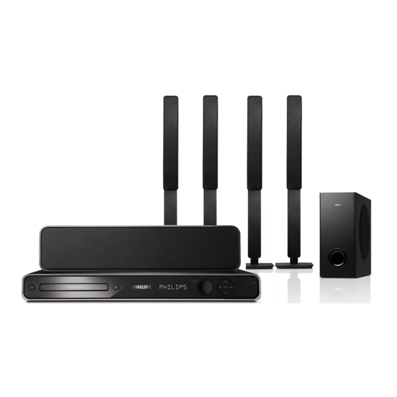
DVD Home Theater System
Service
Service Manual
©
Copyright 2008 Philips Consumer Electronics B.V. Eindhoven, The Netherlands
All rights reserved. No part of this publication may be reproduced, stored in a retrieval system or
transmitted, in any form or by any means, electronic, mechanical, photocopying, or otherwise
without the prior permission of Philips.
Published by
LM0831
Service Audio Printed in The Netherlands Subject to modification
Version 1.0
TABLE OF CONTENTS
Location of PCB Boards ............................................. 1-2
Versions Variation ....................................................... 1-2
Specifications .............................................................. 1-3
Measurement Setup ....................................................1-4
Service Aids ................................................................ 1-5
ESD & Safety Instruction ............................................ 1-6
Lead-free solding Information .................................... 1-7
Setting procedure &Repair Instructions ......................... 2
Disassembly Instructions & Service positions .............. 3
Block & Wiring Diagram ................................................ 4
VFD+JACK+VOL+STANDBY Board .............................5
Main Board .....................................................................6
Power Board ...................................................................7
AMP Board .....................................................................8
Scart Board......................................................................9
Mechanical Exploded View & Parts...............................10
Revision list....................................................................11
1 - 1
Chapte
r
HTS3568
/12/05
GB
3139 785 3437

Related Manuals for Philips HTS3568

Summary of Contents for Philips HTS3568
- Page 1 Revision list..............11 © Copyright 2008 Philips Consumer Electronics B.V. Eindhoven, The Netherlands All rights reserved. No part of this publication may be reproduced, stored in a retrieval system or transmitted, in any form or by any means, electronic, mechanical, photocopying, or otherwise without the prior permission of Philips.
- Page 2 LOCATION OF PCB BOARDS SCART PCB MAIN PCB AMP PCB STANDBY PCB VFD PCB POWER PCB VOL PCB JACK PCB VERSION VARIATION: HTS3568 Type/Versions Features Main (Output Power-1000W) S-Video Out Power Voltage (230V) Power Cord ( fixed ) SERVICE SCNARIO MATRIX: HTS3568 Type/Versions...
- Page 3 1 - 3 SPECIFICATIONS MAIN UNIT AMPLIFIER Power Supply Rating ........220 - 240V; 50Hz Total output power: Power Consumption: ............180 W - Home Theatre mode ........... 1000 W Dimensions ..........435 x 58 x 360 (mm) Frequency Response ......180 Hz – 18 kHz / ±3 dB ...................(w x h x d) Signal-to-Noise Ratio ........>...
- Page 4 1 - 4 MEASUREMENT SETUP Tuner FM Bandpass LF Voltmeter 250Hz-15kHz e.g. PM2534 e.g. 7122 707 48001 RF Generator e.g. PM5326 S/N and distortion meter e.g. Sound Technology ST1700B Use a bandpass filter to eliminate hum (50Hz, 100Hz) and disturbance from the pilottone (19kHz, 38kHz). Use Audio Signal Disc SBC429 4822 397 30184 (replaces test disc 3)
- Page 5 1 - 5...
- Page 6 1 - 6...
- Page 7 1 - 7...
- Page 8 In open model, press “1“ “5“ “9“ on R/C the sofeware upgrade? b) press “ok” button to con rm c) TV will show message as below: Cancel Current model HTS3568/12 Version: 00.12.01_1 Release: 2007.12.19 f) select “OK”, OSD will show: Region Servo: 5B.61.00.00 8032: 05.00.04.06...
- Page 9 2 - 2 2 - 2 REPAIR INSTRUCTIONS (part one)
- Page 10 2 - 3 2 - 3 REPAIR INSTRUCTIONS (part two)
- Page 11 2 - 4 2 - 4 REPAIR INSTRUCTIONS (part three)
- Page 12 3 - 1 3 - 1 DISASSEMBLY INSTRUCTIONS Dismantling of the Front Panel Assemble 3) Loosen 7 screws and remove the Top Cover by lifting the rear portion upwards before sliding it out towards the rear. - 1 screw “A” each on the left & right side as shown in gure 4 1) Open the DVD Tray by using the Open/Close Button while the Set is ON and disconnect the mains supply after removing the Tray - 5 screws “B”...
- Page 13 3 - 2 3 - 2 Dismantling of the Main Board Dismantling of the Scart Board 1) Loosen 2 screws “ F “ on the top of main board as shown in gure 9 1) Loosen 2 screws “I” at the back panel as shown in gure 12 2) Loosen 7 screws “G”...
- Page 14 3 - 3 3 - 3 Dismantling of the DVD Module 1) Loosen 4 screws “L” as shown in gure 15. Figure 15 SERVICE POSITIONS Service position A (main unit) Figure 1 Note:In some service positions the components or copper patterns of one board may risk touching its neighbouring pc boards or metallic parts.
- Page 15 4 - 1 4 - 1 BLOCK DIAGRAM OPTICAL INPUT...
- Page 16 4 - 2 4 - 2 WIRING DIAGRAM OPTICAL IN AMP PCB MAIN PCB POWER PCB DVD LOADER CONTROL PCB...
- Page 17 5 - 1 5 - 1 FTD DISPLAY PIN ASSIGNMENT CONTROL BOARD TABLE OF CONTENTS FTD Display Pin Assignment ............. 5-1 Circuit Diagram ................. 5-2 PCB Layout Top & Bottom View ............5-3 PIN CONNECTION...
- Page 18 5 - 2 5 - 2 CIRCUIT DIAGRAM FB12 D3 LD11 A2 RB12 B1 SN11 B1 TA18 D2 FB13 D3 RB13 A1 TA11 C1 TA20 C2 FB14 D3 RB14 A1 TA12 C1 USB11 D3 FB15 D3 RB15 D3 TA13 D1 VR11 D4 DP11 A3 IC11...
- Page 19 5 - 3 5 - 3 PCB LAYOUT - TOP VIEW LD11 A1 RB12 A1 RB16 A4 TA12 A1 TA18 A4 RB13 A2 RB17 A3 TA13 A4 TA20 A3 DP11 A2 RB14 A1 SN11 A1 TA14 A1 USB11 A4 JK11 A4 RB11 A1 RB15 A4 TA11 A4...
- Page 20 6 - 1 6 - 1 INTERNAL IC DIAGRAM - AS81F641642C MAIN BOARD TABLE OF CONTENTS INTERNAL IC DIAGRAM - MT1389S Internal IC Diagram ................6-1 Circuit Diagram (part one) ..............6-2 Circuit Diagram (part two) ..............6-3 PCB Layout Top View ..............6-4 HMDI 1.2 Tx PCB Layout Bottom View ..............
- Page 21 6 - 2 6 - 2 CIRCUIT DIAGRAM - part one C301 A1 C908 D2 FB312 B1 R329 A3 C302 A1 C909 D2 FB313 B1 R330 A3 C303 B1 C911 D2 FB901 D2 R331 A3 C304 A1 C912 D2 FB905 D1 R332 B3 C305 A2 C918 D2...
- Page 22 6 - 3 6 - 3 CIRCUIT DIAGRAM - part two C0201 C2 C230 D3 C837 A3 FB705 A4 R207 A3 R801 C2 C0202 A3 C231 D3 C838 B3 FB706 A4 R209 B5 R802 A1 C0203 A3 C232 C1 C839 B3 FB707 C2 R210 C5 R803 A1...
- Page 23 6 - 4 6 - 4 PCB LAYOUT - TOP VIEW C0202 A3 C701 A3 CN301 B1 L206 B2 R252 C3 R558 A4 C0207 C2 C703 A3 CN401 C5 L207 B2 R253 B1 R559 A4 C0208 C3 C704 A2 CN701 A1 L701 A2 R271 C3 R602 A2...
- Page 24 6 - 5 6 - 5 PCB LAYOUT - BOTTOM VIEW C0201 B4 C315 CE310 C1 R228 C0203 B4 C323 CE311 B1 R238 C0204 B4 C324 CE312 B1 R269 C0205 C5 C518 CE313 B1 R295 C0206 B5 C519 CE314 A1 R3019 B2 C0209 B4 C520...
-
Page 25: Internal Ic Diagram
7 - 1 7 - 1 INTERNAL IC DIAGRAM - AP3843GMTR UVLO 2.50V INTERNAL BIAS VREF GOOD OUTPUT LOGIC POWER BOARD OVER TEMP PROTECT ERROR COMP LATCH CURRENT SENSE COMPARATOR TABLE OF CONTENTS Internal IC Diagram ................7-1 Circuit Diagram .................. 7-2 PCB Layout Top View ............... - Page 26 7 - 2 7 - 2 CIRCUIT DIAGRAM BD901 A1 C914 A3 C925 B3 C937 B1 C950 B3 C960 C1 C969 C2 CN905 C4 D913 B3 D925 B4 J904 Q906 C3 R9001 B1 R911 A3 R926A A4 R937 B1 R951 B1 R964 B2 R976 C3 R989A C4...
- Page 27 7 - 3 7 - 3 PCB LAYOUT - TOP VIEW BD901 A1 C916 B4 C939 C2 C951 C4 C963 B3 C991 C2 D912 B3 D923 C3 IC904 C3 J911 B2 J918 B3 J926 B4 J934 C4 L906 C4 Q911 B3 R904 B2 R937 B2 R945 B4...
- Page 28 7 - 4 7 - 4 PCB LAYOUT - BOTTOM VIEW C904 B3 C918 A1 C928 C2 C941 C3 C958 B2 C969 C2 D907 B1 D991 C3 R901 A4 R919 B1 R926B B1 R931 B1 R955 C1 R970 C4 R978 B2 R989A C1 ZD905 B1 C906 A1...
- Page 29 8 - 1 8 - 1 INTERNAL IC DIAGRAM - CO4558A SO8 VCC+ AMP BOARD TABLE OF CONTENTS Internal IC Diagram ................8-1 VCC- Circuit Diagram .................. 8-2 PCB Layout Top view ............... 8-3 PCB Layout Bottom View ..............8-4...
-
Page 30: Circuit Diagram
8 - 2 8 - 2 CIRCUIT DIAGRAM C467 C544 Q403 R471 C468 Q404 R472 C469 C601 Q405 R473 C470 C602 Q406 R474 C471 Q407 R475 C472 Q408 R476 C473 Q409 R477 C474 CE401 C3 Q410 R478 C475 CE402 C3 Q411 R479 C476... -
Page 31: Pcb Layout Top View
8 - 3 8 - 3 PCB LAYOUT - TOP VIEW C493 A3 L409 D1 R488 A3 C494 A3 L410 C1 R489 A3 C498 B1 L411 C1 R490 A3 C499 B1 L412 C1 R491 A3 L413 C2 R492 A3 C500 B1 L414 C2 R493 A3 C503 B1... -
Page 32: Pcb Layout Bottom View
8 - 4 8 - 4 PCB LAYOUT - BOTTOM VIEW CE410 C1 R506 A2 CE411 D1 R507 A2 C401 C4 CE412 D1 R509 A3 C402 C4 D401 A2 R511 A3 C403 C4 D402 A2 R515 A3 C404 C4 D403 A3 R522 A2 C405 D2 D404 A3... - Page 33 9 - 1 9 - 1 SCART BOARD TABLE OF CONTENTS Circuit Diagram ................. 9-2 PCB Layout View ................9-3...
- Page 34 9 - 2 9 - 2 CIRCUIT DIAGRAM C710 A1 C711 A1 C712 C2 C713 B2 C714 B2 C715 A2 FB707 B2 FB708 B2 FB709 B2 FB710 A2 FB711 A2 FB714 C2 JK703 A2 R707 A2 R708 A2 RB701 B1 RB702 A3...
- Page 35 9 - 3 9 - 3 PCB LAYOUT - TOP VIEW C710 C711 C712 C713 C714 C715 FB707 B2 FB708 B2 FB709 B3 FB710 B1 FB711 B1 FB714 B3 JK703 A2 R707 R708 RB701 B3 RB702 B1...
- Page 36 10 - 1 10 - 1 MECHANICAL EXPLODED VIEW Note: A1=14+15+35+37...
- Page 37 10 - 2 10 - 2 MECHANICAL PART LIST Loc. 12NC. Description 996510012484 DISPLAY LENS PMMA 996510012485 USB DOOR LENS 996510010835 SOURCE BUTTON PC PMMA 996510010833 VOLUME KNOB PMMA PC 996510010832 FUNCTION BUTTON 996510010829 USB DOOR 996510012215 FRONT PANEL 996510010837 FUNCTION BRACKET 996510010834 EJECT KEY...
- Page 38 11 - 1 11 - 1 REVISION LIST Version 1.0 *Initial release...