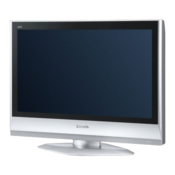
Panasonic TC-26LX60C Service Manual
Chassis: lh58
Hide thumbs
Also See for TC-26LX60C:
- Operating instructions manual (101 pages) ,
- Manual de instrucciones (35 pages) ,
- Operating instructions manual (32 pages)
Table of Contents
Quick Links
CONTENTS
7.2. Adjustment method.....Use the remote control.
TC-26LX60C
TC-32LX60C
LH58
Page
3
3
3
4
5
6
7
8
8
8
8
8
8
8
8
8
© 2006 Panasonic Corporation of North America. All
rights
distribution is a violation of law.
MTNC060582CE
B05 Canada: B07
LCD TV
reserved.
Unauthorized
copying
Page
8
11
12
12
13
14
14
15
16
17
18
19
19
21
22
22
and
Table of Contents

Related Manuals for Panasonic TC-26LX60C


Summary of Contents for Panasonic TC-26LX60C
-
Page 1: Table Of Contents
13.2. Block Diagram for P and AP (DC-DC CONV.) (2 of 2) 8.2. How to access 14 Schematic Diagrams 8.3. Screen Display 14.1. Schematic Diagram Notes © 2006 Panasonic Corporation of North America. All rights reserved. Unauthorized copying distribution is a violation of law. - Page 2 14.2. Reference of PDF links color 14.14. V-Board Schematic Diagram 14.3. A-Board (1 of 8) Schematic Diagram 14.15. G-Board Schematic Diagram 14.4. A-Board (2 of 8) Schematic Diagram 15 Printed Circuit Boards 14.5. A-Board (3 of 8) Schematic Diagram 15.1. A-Board Top Side 14.6.
-
Page 3: Safety Precautions
1 Safety precautions 2 Warning General guidelines 2.1. Prevention of Electro Static 1. When servicing, observe the original lead dress. If a Discharge (ESD) to short circuit is found, replace all parts which have been Electrostatically Sensitive (ES) overheated or damaged by the short circuit. 2. -
Page 4: About Lead Free Solder (Pbf)
3 About lead free solder (PbF) NOTE Lead is listed as (Pb) in the periodic table of elements. In the information below, Pb will refer to lead solder, and PbF will refer to Lead Free Solder. The lead free solder used in our manufacturing process and discussed below is (Sn+Ag+Cu). That is Tin (Sn), Silver (Ag) and Copper (Cu) although other types are available. -
Page 5: Receiver Feature Table
4 Receiver feature table FEATURE / MODEL TC-26LX60C TC-32LX60C LCD TYPE IPS (WXGA) IPS (WXGA) LCD PANEL MAKER CHASSIS LH58 LH58 SYSTEM NTSC NTSC TUNING STEREO MTS/SAP MTS/SAP CATV USA CATV 181CH USA CATV 181CH POWER SUPPLY AC120-127V, 60HZ AC120-127V, 60HZ... -
Page 6: Chassis Board Layout
5 Chassis Board Layout Board Layout Board Name TC-26LX60C TC-32LX60C Function A-Board TZRXN010MQJE TZRXN010MPJE Main (AV Switch, Audio, MCU, Global Core, AV connector) AP-Board TZRXN020MPJE TZRXN020MPJE DC-DC G-Board TNPA3784S Side Terminal V-Board TNPA3749ACS Remote Reciever, LED P-Board N0AB3GJ00010 AC-DC... -
Page 7: Location Of Controls (Eur7613Z90R Or Eur7613Ze0)
6 Location of controls (EUR7613Z90R or EUR7613ZE0) -
Page 8: Service Mode
7 Service Mode can be used to confirm the occurrence and to limit the scope for the defective circuits. Also, when "the power fails from time to time", display on the screen can be used to 7.1. How to enter into adjustment confirm the occurrence and to limit the scope for the mode defective circuits. - Page 9 Without the back cover then remove the screws indicated on the figure above by arrows. Bracket Disassembly 1. To remove the bracket shown above remove the screws indicated on the figure above by arrow. A-Board Disassembly 1. First remove the two screws from each bracket one located on top and one on the bottom.
- Page 10 Speaker Disassembly 1. To remove the speaker remove the screws indicated on the figure by arrows, each speaker is located on sides. V-Board Disassembly 1. To remove the V-Board remove the screws indicated on the figure by arrows. Removing the pedestal 1.
-
Page 11: Removing The Lcd Panel Assembly And Lcd L/R Mtg
9.1. Removing the LCD panel assembly and LCD L/R MTG 1. Remove the 4 screws. 2. Remove the LCD panel ass’y and LCD L/R MTG. 9.2. Removing the LCD panel and LCD T/B MTG 1. Remove the 4 screws. 2. Remove the LCD panel and LCD T/B MTG. -
Page 12: Measurements And Adjustments
10 Measurements and Adjustments 10.1. White Balance Adjustment... -
Page 13: Mts Circuit Adjustment
minimum for both signals. 11 MTS circuit adjustment The MTS circuit adjustment require two steps: 1. Input level adjustment. 2. Stereo separation adjustment. Input level adjustment Service DAC adjustment (MTSIN) PREPARATION 1. Connect an RMS meter with filter jig as shown in figure to TP1105 or TP1107 and gound. -
Page 14: Boards Assemblies
12 Boards Assemblies 12.1. AP-Board... -
Page 15: A-Board
12.2. A-Board... -
Page 16: P-Board
12.3. P-Board... -
Page 17: G-Board
12.4. G-Board... -
Page 18: V-Board
12.5. V-Board... -
Page 19: Block Diagram
13 Block Diagram 13.1. Block Diagram for P and AP (DC-DC CONV.) (1 of 2) - Page 20 AP DC-DC CONV. IC7218 SOUND_20V OVP SOUND_20V Q7210 D7303 D7304 SHORT SOS +20V (+22V) L:NORMAL H:ABNORMAL KEY SCAN Q7301 Note: SOUND+18V ON 10V, BT30V K-board is included in the control panel assy. SOUND VCC,PAN 5V OVP SHORT SOS IC7205 D7301 D7302 KEY SCAN MAIN_5V...
-
Page 21: Block Diagram For P And Ap (Dc-Dc Conv.) (2 Of 2)
13.2. Block Diagram for P and AP (DC-DC CONV.) (2 of 2) SOUND_VCC SOUND_VCC *D7220 BT_30V MAIN_9V 10V SHORT SOS MAIN_9V D_20V OVP Q7210 MAIN_9V D7208 D7304 SHORT SOS MAIN_5V MAIN_5V BT 30V SHORT SOS L:NORMAL D7471 D7469 H:ABNORMAL D7207 SOUND VCC SHORT SOS Q7211 10V, BT30V... -
Page 22: Schematic Diagrams
14 Schematic Diagrams 14.1. Schematic Diagram Notes... -
Page 23: Reference Of Pdf Links Color
14.2. Reference of PDF links color... -
Page 24: A-Board (1 Of 8) Schematic Diagram
14.3. A-Board (1 of 8) Schematic Diagram " & )3*4)5,666666!6786(6666669:;0<&'')0=)+666669+3"&>?&<+@69+3#">?&<+... -
Page 25: A-Board (2 Of 8) Schematic Diagram
14.4. A-Board (2 of 8) Schematic Diagram " & )3*4)5,666666"6786(6666669:;0<&'')0=)+666669+3"&>?&<+@69+3#">?&<+... -
Page 26: A-Board (3 Of 8) Schematic Diagram
14.5. A-Board (3 of 8) Schematic Diagram " & )3*4)5,666666#6786(6666669:;0<&'')0=)+666669+3"&>?&<+@69+3#">?&<+... -
Page 27: A-Board (4 Of 8) Schematic Diagram
14.6. A-Board (4 of 8) Schematic Diagram " & )3*4)5,666666$6786(6666669:;0<&'')0=)+666669+3"&>?&<+@69+3#">?&<+... -
Page 28: A-Board (5 Of 8) Schematic Diagram
14.7. A-Board (5 of 8) Schematic Diagram " & )3*4)5,666666%6786(6666669:;0<&'')0=)+666669+3"&>?&<+@69+3#">?&<+... -
Page 29: A-Board (6 Of 8) Schematic Diagram
14.8. A-Board (6 of 8) Schematic Diagram " & )3*4)5,666666&6786(6666669:;0<&'')0=)+666669+3"&>?&<+@69+3#">?&<+... -
Page 30: A-Board (7 Of 8) Schematic Diagram
14.9. A-Board (7 of 8) Schematic Diagram " & )3*4)5,666666'6786(6666669:;0<&'')0=)+666669+3"&>?&<+@69+3#">?&<+... -
Page 31: A-Board (8 Of 8) Schematic Diagram
14.10. A-Board (8 of 8) Schematic Diagram " & )3*4)5,666666(6786(6666669:;0<&'')0=)+666669+3"&>?&<+@69+3#">?&<+... -
Page 32: Ap-Board (1 Of 3) Schematic Diagram
14.11. AP-Board (1 of 3) Schematic Diagram " & );3*4)5,6666666!6786#6666669:;)#($A)+66666669+3"&>?&<+@69+3#">?&<+... -
Page 33: Ap-Board (2 Of 3) Schematic Diagram
14.12. AP-Board (2 of 3) Schematic Diagram " & );3*4)5,6666666"6786#6666669:;)#($A)+66666669+3"&>?&<+@69+3#">?&<+... -
Page 34: Ap-Board (3 Of 3) Schematic Diagram
14.13. AP-Board (3 of 3) Schematic Diagram " & );3*4)5,666666#6786#6666669:;)#($A)+66666669+3"&>?&<+@69+3#">?&<+... -
Page 35: V-Board Schematic Diagram
14.14. V-Board Schematic Diagram " & B3*4)5,66666669:;)#'$A)+66666669+3"&>?&<+@69+3#">?&<+... -
Page 36: G-Board Schematic Diagram
14.15. G-Board Schematic Diagram... - Page 37 " & /3*4)5,66666669:;)#'($66666669+3"&>?&<+@69+3#">?&<+...
-
Page 38: Printed Circuit Boards
15.1. A-Board Top Side 15 Printed Circuit Boards " & )3*4)5,66666669:;0<&''33666694;66669+3"&>?&<+@69+3#">?&<+... -
Page 39: A-Board Bottom Side
15.2. A-Board Bottom Side " & )3*4)5,66666669:;0<&''336666*4994C66669+3"&>?&<+@69+3#">?&<+... -
Page 40: Ap-Board
15.3. AP-Board Q7901 R7352 AP11 C7904 C7905 TP7502 R7907 C7906 R7905 L7962 R7504 R7906 R7506 L7501 Q7504 R7346 R7509 D7904 D7903 Q7506 R7347 D7208 R7234 L7203 C7966 D7205 L7956 R7310 D7469 D7478 R7486 C7349 C7961 D7231 C7958 R7247 R7218 C7967 R7228 C7226 C7956... -
Page 41: G-Board
15.4. V & G-Board R014 R026 Q004 R019 R003 CR NO.1 Q003 Q008 D005 R031 Q006 R016 TNPA3749 1 V R027 R032 R021 C005 R025 C001 R013 C002 R018 R012 RM001 R009 R017 SN001 C004 SEE REVERSE FOR ORDER NO. R029 C009 R030... -
Page 42: Parts Location
16 Parts Location LCD TV Exploded View 16.1. Packing Exploded View Package contents... -
Page 43: Parts List
17 Parts list 17.1. Description of abbreviations guide... -
Page 44: Parts List
17.2. Parts list Note: All parts except parts mentioned [PAVCA] in the Ref. Part No. Part Name & Remarks Safeyma Remarks column are supplied by PAVC-CSG. Description Parts mentioned [PAVCA] are supplied by PAVCA. C1885 ECJ3YB1C475K C 0.047UF K 16V C1886 ECJ1VB1E272K C 2700PF K 25V... - Page 45 Ref. Part No. Part Name & Remarks Safeyma Ref. Part No. Part Name & Remarks Safeyma Description Description C2169 EEEHB1C220UR C 22PF J 16V C4036 ECJ1VB1A105K C 0.01UF Z 50V C2170 ECJ3XB1C106M C 1.0UF K 16V C4037 ECJ1VB1A105K C 0.01UF Z 50V C2171 EEEHB1C101UP C 100PF J 16V...
- Page 46 Ref. Part No. Part Name & Remarks Safeyma Ref. Part No. Part Name & Remarks Safeyma Description Description C4129 ECJ2FB0J106M C 10UF Z 6.3V C7209 F2A1C101A121 E 100UF 16V C4139 ECJ0EB1H102K C 1000PF K 50V C7210 ECJ2VB1C224K C 0.22UF K 16V C4140 ECJ0EB1H102K C 1000PF K 50V...
- Page 47 MA8140M ZENER DIODE FL5001 F1J1A1050020 C 1UF Z 50V D3805 MA8140M ZENER DIODE INTEGRATED CIRCUITS D3806 MA8140M ZENER DIODE IC1102 TVRN925S IC TC-26LX60C PAVCA D3809 MA8140M ZENER DIODE IC1102 TVRN924S IC TC-32LX60C PAVCA D3810 MA8140M ZENER DIODE IC1803 C0EBF0000354 D3811...
- Page 48 Ref. Part No. Part Name & Remarks Safeyma Ref. Part No. Part Name & Remarks Safeyma Description Description L4004 J0JHC0000078 CHIP INDUCTOR Q3862 B1ABCE000015 TRANSISTOR L4005 J0JHC0000078 CHIP INDUCTOR Q4001 B1ABCE000015 TRANSISTOR L4006 J0JHC0000078 CHIP INDUCTOR Q4002 B1ADDF000005 TRANSISTOR L4007 J0JHC0000078 CHIP INDUCTOR Q4003...
- Page 49 Ref. Part No. Part Name & Remarks Safeyma Ref. Part No. Part Name & Remarks Safeyma Description Description R001 ERJ2GEJ102 M 1KOHM J 0.063W R1848 ERJ3GEYJ563 M 56KOHM J 1/16W R003 ERJ3GEYJ271 M 270 OHM J 1/16W R1849 ERJ3GEYJ154 M 150KOHM J 1/16W R004 ERJ3GEYJ331 M 330 OHM J 1/16W...
- Page 50 Ref. Part No. Part Name & Remarks Safeyma Ref. Part No. Part Name & Remarks Safeyma Description Description R2160 ERJ2GEJ104 M 100KOHM J 0.063W R3110 ERJ3GEY0R00 M 0 OHM 1/16W R2161 ERJ2GEJ473 M 47KOHM J 0.063W R3111 ERJ3GEY0R00 M 0 OHM 1/16W R2208 ERJ2GEJ222 M 2.2KOHM J 0.063W...
- Page 51 Ref. Part No. Part Name & Remarks Safeyma Ref. Part No. Part Name & Remarks Safeyma Description Description R4048 ERJ3GEYJ101 M 100 OHM J 1/16W R4192 ERJ3GEYJ103 M 10KOHM J 1/16W R4049 ERJ3GEYJ101 M 100 OHM J 1/16W R4193 ERJ3GEYJ103 M 10KOHM J 1/16W R4050 ERJ3GEYJ101...
- Page 52 Ref. Part No. Part Name & Remarks Safeyma Ref. Part No. Part Name & Remarks Safeyma Description Description R4280 ERJ3GEYJ221 M 220 OHM J 1/16W R5096 ERJ3GEYJ104 M 100KOHM J 1/16W R4281 ERJ3GEYJ332 M 3.3KOHM J 1/16W R5097 ERJ3GEYJ473 M 47KOHM J 1/16W R4282 ERJ3GEYJ332 M 3.3KOHM J 1/16W...
- Page 53 FERRITE CORE 26LX60C M004 K0RB00500001 CONTROL PANEL ASSY PAVCA (CIRCUIT BOARD&PANERL) M005 K2CB2DZ00015 AC CORD M006 L5EDD6Q00014 LCD PANEL TC-26LX60C PAVCA M007 L5EDD8Q00020 LCD PANEL TC-32LX60C PAVCA M008 TBLA0194 PEDESTAL ASS’Y PAVCA M009 TBMA180 PANASONIC BADGE M010 TBX2AA3501 POWER BUTTON...