Sony CDX-656 Service Manual
Hide thumbs
Also See for CDX-656:
- Operating instructions (3 pages) ,
- Product manual (2 pages) ,
- Limited warranty (1 page)
Table of Contents
Quick Links
SERVICE MANUAL
Ver. 1.1 2006.03
Sony Corporation
9-873-375-02
2006C05-1
eVehicle Division
© 2006.03
Published by Sony Techno Create Corporation
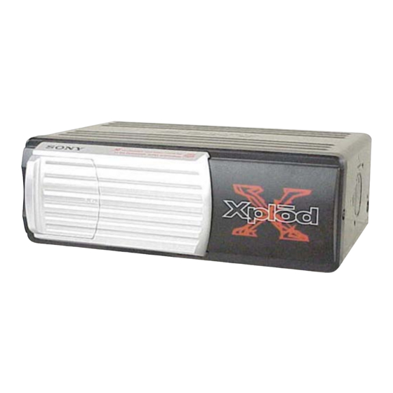
CDX-656/656X
Photo: CDX-656X
Model Name Using Similar Mechanism
CD Drive Mechanism Type
Optical Pick-up Name
SPECIFICATIONS
System
Compact disc digital audio system
Laser diode properties Material: GaAlAs
Wavelength: 780 nm
Emission Duration: Continuous
Laser out-put Power: Less than
44.6 µW*
* This output is the value measured at a distance of 200 mm
from the objective lens surface on the Optical Pick-up Block.
Frequency response
10 – 20,000 Hz
Wow and flutter
Below the measurable limit
Signal-to-noise ratio
94 dB
Outputs
BUS control output (8 pins)
Analog audio output (RCA pin)
Current drain
800 mA (during CD playback)
800 mA (during loading or ejecting
a disc)
Operating temperature –10°C to +55°C (14°F to 131°F)
Approx. 262 × 90 × 185 mm
Dimensions
/8 × 3
/8 × 7
(10
3
5
(w/h/d) not incl. projecting parts
and controls
Mass
Approx. 2.1 kg (4 lb. 10 oz.)
Power requirement
12 V DC car battery
(negative ground)
Supplied accessories
Disc magazine (1)
Parts for installation and
connections (1 set)
Design and specifications are subject to change without
notice.
Canadian Model
Chinese Model
3
/8 in.)
COMPACT DISC CHANGER
US Model
AEP Model
UK Model
CDX-656
E Model
CDX-656X
CDX-646/646X
MG-251B-137
KSS-720A or KSS-721A
Table of Contents

Related Manuals for Sony CDX-656


Summary of Contents for Sony CDX-656
- Page 1 (negative ground) Supplied accessories Disc magazine (1) Parts for installation and connections (1 set) Design and specifications are subject to change without notice. COMPACT DISC CHANGER Sony Corporation 9-873-375-02 2006C05-1 eVehicle Division © 2006.03 Published by Sony Techno Create Corporation...
-
Page 2: Servicing Notes
LES DIAGRAMMES SCHÉMATIQUES ET LA LISTE DES PIÈCES SONT CRITIQUES POUR LA SÉCURITÉ DE FONCTIONNEMENT. NE REMPLACER CES COM- POSANTS QUE PAR DES PIÈCES SONY DONT LES NUMÉROS SONT DONNÉS DANS CE MANUEL OU DANS LES SUPPLÉMENTS PUBLIÉS PAR SONY. -
Page 3: Table Of Contents
CDX-656/656X Ver. 1.1 TABLE OF CONTENTS CAUTION Use of controls or adjustments or performance of procedures SERVICING NOTES ............2 other than those specified herein may result in hazardous ra- diation exposure. GENERAL ..............4 Installation ............... 5 Flexible Circuit Board Repairing Connections .............. -
Page 4: General
CDX-656/656X SECTION 1 This section is extracted from instruction manual. GENERAL Inserting a disc Insertion d’un disque Inserción de discos Push to unlock the door Use the supplied disc magazine or the disc Poussez pour déverrouiller la porte magazine XA-250.The disc magazine XA-10B/XA-... -
Page 5: Installation
• Make holes of ø 3.5 mm ( • Utilisez uniquement les vis fournies. in.) only after making sure there is nothing on the Sony BUS compatible car audio • Ne percez les trous de 3,5 mm ( suministrada. other side of the mounting surface. -
Page 6: Disassembly
CDX-656/656X Ver. 1.1 SECTION 2 DISASSEMBLY • This set can be disassembled in the order shown below. Note: Follow the disassembly procedure in the numerical order given. 2-1. DISASSEMBLY FLOW 2-2. CASE (UPPER. T), FRONT PANEL ASSY 3 screw (PTT2.6 × 6) Note 1: The process described in can be performed in any order. -
Page 7: Jack Board
CDX-656/656X 2-4. JACK BOARD Remove the jack board of the arrow. 1 ground point screw (PTT2.6 × 6) 2 jack board 2-5. MAIN BOARD, SLIDE VARIABLE RESISTOR (ELEVATOR HEIGHT SENSOR) (RV202) 1 main flexible board (CNJ101) 5 two screws (FP) -
Page 8: Elj Motor Assy (Elevator) (M104)
CDX-656/656X 2-6. ELJ MOTOR ASSY (ELEVATOR) (M104) 1 screw (PTT2 × 4) 2 bracket (EVM.S) 3 ELJ motor assy (elevator) (M104) 2-7. ESCUTCHEON (T) 3 two claws 2 Remove the claw in the direction of arrow A . 4 Remove the ditch in the direction of arrow B . -
Page 9: Chassis (U.s) Sub Assy
CDX-656/656X 2-8. CHASSIS (U.S) SUB ASSY 2 Remove the edge in the direction 1 three screws of arrow A . (PTT2 × 4) 1 two screws (PTT2 × 4) 5 chassis (U.S) sub assy 1 screw (PTT2 × 4) 4 spring (SUT) 2-9. -
Page 10: Rf Board
CDX-656/656X Ver. 1.1 2-10. RF BOARD 3 two screws (PS2 × 4) 4 RF board 3 two screws (PS2 × 4) 2 Remove four solders of the LSW board leads and spindle motor leads (M102). 2 Remove two solders of the sled motor leads 1 OP flexible board (CN102). -
Page 11: Lsw Board, Spindle Motor (S) Sub Assy (M102)
CDX-656/656X 2-12. LSW BOARD, SPINDLE MOTOR (S) SUB ASSY (M102) 8 two precision screws (P1.7 × 2.2) 3 spring (chucking) 6 retainer (disc) 1 precision screw (P2 × 2.5) 4 precision screw (P2 × 2.2) 5 bracket (CP) 2 LSW board 9 Remove the spindle motor (S) sub assy (M102) in the direction of the arrow. -
Page 12: Assembly
CDX-656/656X SECTION 3 ASSEMBLY • This set can be assembled in the order shown below. 3-1. ASSEMBLY FLOW 3-2. OPTICAL PICK-UP COMPLETE ASSY (Page 12) 3-3. GEAR (LOMINI) / (LOAD 1) ASSY (Page 13) 3-4. OPERATION CHECK (Page 13) 3-2. -
Page 13: Gear (Lomini)/(Load 1) Assy
CDX-656/656X 3-3. GEAR (LOMINI)/(LOAD 1) ASSY gear (LOAD 2) 2 Attach the gear (LOMINI) at the position shown in Fig. A. gear (LOMINI) shaft (rotary prevention C) chuck plate 1 Move the lever (LOCK 3A) fully in the direction of arrow B to move the chuck plate up. -
Page 14: Mechanical Adjustment
CDX-656/656X SECTION 4 MECHANICAL ADJUSTMENT • Elevator Height (Address) Adjustment Adjustment Method: Note: This adjustments is necessary when the system controller (IC201), variable resistor (RV201), slider (R), slider (L), or chassis (ELV) 1. Connect this set to the master unit (e.g. MDX-C7970/C7970R), was replaced for any repair. -
Page 15: Electrical Check
CDX-656/656X SECTION 5 ELECTRICAL CHECK Note: Focus Bias Check 1. This check is performed with the set placed horizontally. 2. Power supply voltage: DC14.4 V (more than 3 A). Connection: 3. Be sure to use the disc “YEDS-18” parts code: 3-702-101-01, but only –... - Page 16 CDX-656/656X Tracking Offset Check Connection: – RF Board (Component Side) – oscilloscope (DC range) – TP (VC) IC101 TP (TE) Procedure: 1. Connect the oscilloscope to TP (TE) and TP (VC) on the RF board. 2. Put the set into play mode by loading the disc (YEDS-18).
-
Page 17: Diagrams
CDX-656/656X Ver. 1.1 SECTION 6 DIAGRAMS 6-1. BLOCK DIAGRAM – SERVO Section – FILTER RF AMP, 53 56 55 FOCUS/TRACKING ERROR AMP IC101 CN901 (1/2) DETECTOR AOUT1 AIN1 LOUT1 SERIAL RFAC GROUND- RFAC RFAC RF EQ RFAC ASYMMENTRY DIGITAL DIGITAL FILTER,... -
Page 18: Block Diagram - Bus Control/Power Supply Section
RESET SIGNAL CN901 (2/2) RESET GENERATOR IC303 CONTROL PS901 +3.3V B. UP +3.3V REGULATOR B. UP Q303, 305 BUS INTERFACE (FOR SONY BUS) IC302 DATA UNI SI DATA UNI SO UNI CK BUSON OUT BUSON BUSON BUSON OUT BUSON IN RESET... -
Page 19: Note For Printed Wiring Boards And Schematic Diagrams
CDX-656/656X Ver. 1.1 6-3. NOTE FOR PRINTED WIRING BOARDS AND SCHEMATIC DIAGRAMS • Waveforms – RF Board – – MAIN Board – Note on Printed Wiring Board: Note on Schematic Diagram: • X : parts extracted from the component side. -
Page 20: Printed Wiring Boards - Rf/Lsw Boards
CDX-656/656X 6-4. PRINTED WIRING BOARDS – RF/LSW Boards – Ver. 1.1 • Semiconductor Location Ref. No. Location IC101 IC201 Q101 Q102 M101 (SLED) M103 (CHUKING) OPTICAL PICK-UP BLOCK (KSS-720A OR KSS-721A) OP FLEXIBLE BOARD (RFAC) (VC) (TE) MAIN FLEXIBLE BOARD... -
Page 21: Schematic Diagram - Rf/Lsw Boards
CDX-656/656X Ver. 1.1 6-5. SCHEMATIC DIAGRAM – RF/LSW Boards – • • See page 19 for for Waveforms. See page 27 for IC Block Diagrams. Q101 MSB709 -RT1 Q102 MUN2212T1 (Page 24) -
Page 22: Printed Wiring Boards - Main Board (Component Side)
CDX-656/656X 6-6. PRINTED WIRING BOARDS – MAIN Board (Component Side) – • Semiconductor Location Ref. No. Location MAIN BOARD D301 (COMPONENT SIDE) D304 D305 D306 D307 C109 D310 C105 C104 D312 C108 C110 C107 IC101 C106 IC201 C112 IC301 IC302... -
Page 23: Printed Wiring Boards - Main (Conductor Side)/Switch Boards
CDX-656/656X 6-7. PRINTED WIRING BOARDS – MAIN (Conductor Side)/SWITCH Boards – • Semiconductor Location Ref. No. Location MAIN BOARD (CONDUCTOR SIDE) IC304 H-12 IC305 F-12 (CHASSIS) 1-681-576- (11) (CHASSIS) SWITCH BOARD SW801 1-681-578- (11) (CHASSIS) -
Page 24: Schematic Diagram - Main Board (1/2)
CDX-656/656X 6-8. SCHEMATIC DIAGRAM – MAIN Board (1/2) – • • See page 19 for for Waveforms. See page 27 for IC Block Diagram. C101 R114 SCOR SQSO COUT LMUT TP101 MIRR RMUT R501 C503 DFCT AVDD2 0.001 TP102 AOUT2... -
Page 25: Schematic Diagram - Main (2/2)/Switch Boards
(CHASSIS) TP322 TP324 IC302 BA8272AFV-E2 R301 RESET ELEVATOR MOTOR DRIVE DATA VREF IC301 LB1930M-TLM BUSON BUSON BUSON BUS INTERFACE TP305 (FOR SONY BUS) TP306 JACK TP307 DATA FLEXIBLE TP308 BUSON BOARD TP309 C301 C302 C303 C304 D304 D301 D305 C306... -
Page 26: Printed Wiring Boards - Jack Board
6-10. PRINTED WIRING BOARDS – JACK Board – 6-11. SCHEMATIC DIAGRAM – JACK Board – JACK BOARD (COMPONENT SIDE) C906 JACK FLEXIBLE BOARD MAIN BOARD CN301 (Page 22) (Page 25) 1-681-577- (11) AUDIO OUT JACK BOARD (CONDUCTOR SIDE) CONTROL (FOR SONY BUS) 1-681-577- (11) - Page 27 CDX-656/656X • IC Block Diagrams – RF Board – IC101 CXA2581N-T4 RW/ROM DC OFST RFDCI – – RFDCO – RW/ROM VOFST APC AMP EQ ON/OFF RFAC EQ IN RW/ROM RFAC AC SUM SUMMING VOFST – – RW/ROM TE BAL RW/ROM –...
- Page 28 CDX-656/656X IC201 LA6576L-TE-L S-GND THERMAL SHUT DOWN CH2-4 INPUT MUTE2 MUTE VCC2 MUTE1 MUTE VLO– OUTPUT VIN4 CONTROL VIN4– VLO+ VO4+ VIN4+ LEVEL SHIFT VO4– VREF-IN VIN1/VREF VIN1 (VREF)-SW SWITCH VO3+ LEVEL VREF-OUT (CH1) SHIFT 5VREG VO3– – REG-OUT –...
- Page 29 CDX-656/656X – MAIN Board – IC101 CXD3017Q ERROR DIGITAL CORRECTOR ASYMMETRY DIGITAL CORRECTOR OPERATIONAL LRCK AMPLIFIER ANALOG SWITCH PCMD INTERFACE DEMODULATOR CONVERTER EMPH XVDD XTAI TIMING CLOCK LOGIC XTAO XTSL GENERATOR XVSS TES1 AVDD1 TEST AOUT1 SERVO DSP PWM GENERATOR...
-
Page 30: Ic Pin Function Description
Serial data reading clock signal output to the CXD3017Q SENS Internal status signal (sense signal) input BUSON Bus on/off control signal input from the SONY bus interface “H”: bus on Battery detection signal input “L”: battery on BUCHK 47, 48 MD0, MD1 Setting terminal for the CPU operational mode (fixed at “H”... - Page 31 Two-way data bus terminal Not used RAMIO3 System reset signal input from the SONY bus interface and reset signal generator “L”: reset RESET For several hundreds msec. after the power supply rises, “L” is input, then it changes to “H”...
- Page 32 CDX-656/656X Pin No. Pin Name Description Chucking end detect switch input terminal LOAD SW “L”: When completion of the disc chucking operation Sled limit in detect switch input terminal LIM SW “L”: When the optical pick-up is inner position RW SEL CD-ROM/RW selection signal output “L”: CD-RW, “H”: CD-ROM...
-
Page 33: Exploded Views
X-3375-360-2 ARM (FRT) ASSY 1-681-578-11 SWITCH BOARD RV202 1-227-137-12 RES, VAR, SLIDE 10K (ELEVATOR HEIGHT SENSOR) X-3379-707-1 DOOR (L) ASSY (CDX-656) X-3381-481-1 DOOR (L) ASSY (CDX-656X) 7-685-792-09 SCREW +PTT 2.6X6 (S) 3-224-392-12 PANEL (L), FRONT (CDX-656X) 7-685-781-09 SCREW +PTT 2X4 (S) -
Page 34: Mechanism Deck Section-1 (Mg-251B-137)
CDX-656/656X 7-2. MECHANISM DECK SECTION-1 (MG-251B-137) mechanism deck section-3 mechanism deck section-2 Ref. No. Part No. Description Remark Ref. No. Part No. Description Remark X-3378-091-2 CHASSIS (U. S) SUB ASSY 3-011-997-01 SPRING (STOPPER. LOWER) 3-024-161-01 SPRING (SUT) 7-685-781-09 SCREW +PTT 2X4 (S) -
Page 35: Mechanism Deck Section-2 (Mg-251B-137)
CDX-656/656X 7-3. MECHANISM DECK SECTION-2 (MG-251B-137) M104 Ref. No. Part No. Description Remark Ref. No. Part No. Description Remark 3-024-170-01 SPRING (SB), TENSION M104 A-3301-123-A ELJ MOTOR ASSY (ELEVATOR) * 152 3-040-790-03 BRACKET (EVM. S) 7-685-781-09 SCREW +PTT 2X4 (S) -
Page 36: Mechanism Deck Section-3 (Mg-251B-137)
CDX-656/656X Ver. 1.1 7-4. MECHANISM DECK SECTION-3 (MG-251B-137) mechanism deck section-4 M103 Ref. No. Part No. Description Remark Ref. No. Part No. Description Remark * 201 3-024-150-01 RETAINER (CHM) * 211 A-3290-194-N MAIN ASSY, CHASSIS (EVY) * 202 X-3378-080-1 BRACKET (CHM. D) ASSY... -
Page 37: Mechanism Deck Section-4 (Mg-251B-137)
CDX-656/656X Ver. 1.1 7-5. MECHANISM DECK SECTION-4 (MG-251B-137) not supplied M102 not supplied M101 not supplied Note: When exchanging the Ref No. 255, 261, refer to “DISCRIMINATION OF OPTICAL PICK-UP” (page 3) on the SERVICING NOTES without fail. Ref. No. -
Page 38: Electrical Parts List
CDX-656/656X Ver. 1.1 SECTION 8 The components identified by mark ELECTRICAL PARTS LIST JACK MAIN 0 or dotted line with mark 0 are critical for safety. NOTE: Replace only with part number • Due to standardization, replacements in the • Items marked “*” are not stocked since they specified. - Page 39 CDX-656/656X MAIN Ref. No. Part No. Description Remark Ref. No. Part No. Description Remark C504 1-162-964-11 CERAMIC CHIP 0.001uF R304 1-216-847-11 METAL CHIP 150K 1/10W C505 1-124-589-11 ELECT 47uF R305 1-216-845-11 METAL CHIP 100K 1/10W C506 1-124-589-11 ELECT 47uF R306...
- Page 40 CDX-656/656X Ver. 1.1 SWITCH Ref. No. Part No. Description Remark Ref. No. Part No. Description Remark C105 1-126-206-11 ELECT CHIP 100uF 6.3V R208 1-216-839-11 METAL CHIP 1/16W C106 1-164-156-11 CERAMIC CHIP 0.1uF R209 1-216-833-11 METAL CHIP 1/16W C107 1-164-156-11 CERAMIC CHIP 0.1uF...
- Page 41 CDX-656/656X Ref. No. Part No. Description Remark Ref. No. Part No. Description Remark PARTS FOR INSTALLATION AND CONNECTIONS ************************************** 3-040-583-21 BRACKET (T) * 502 X-3369-824-1 SCREW ASSY 1-824-929-11 CORD, CONNECTION (RCA PIN CORD 5m) 1-590-519-21 CORD (WITH CONNECTOR) (BUS CABLE 5m) +PSW4 ×...
-
Page 42: Revision History
CDX-656/656X REVISION HISTORY Clicking the version allows you to jump to the revised page. Also, clicking the version at the upper right on the revised page allows you to jump to the next revised page. Ver. Date Description of Revision 2001.11...