Table of Contents
Table of Contents

Related Manuals for Emerson 6513DE


Summary of Contents for Emerson 6513DE
-
Page 1: Service Manual
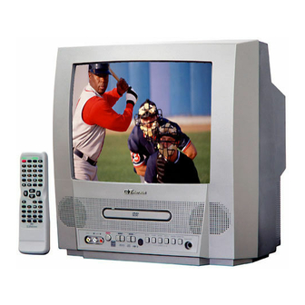
SERVICE MANUAL 13" COLOR TV/DVD 6513DE EWC13D4 MSD513E... -
Page 2: Table Of Contents
IMPORTANT SAFETY NOTICE Proper service and repair is important to the safe, reliable operation of all Funai Equipment. The service procedures recommended by Funai and described in this service manual are effective methods of performing service operations. Some of these service special tools should be used when and as recommended. -
Page 3: Specifications
SPECIFICATIONS < TV Section > *Test input terminal-------------Video input (1Vp-p) Audio input (-10dB) -----------------------Ant. input (80dBµV) Video: 87.5% Audio: 25kHz dev (1kHz Sin) Description Condition Unit Nominal Limit 1. Over Scan — — Horizontal — 2. Linearity Vertical —... -
Page 4
ITEM CONDITIONS UNIT NOMINAL LIMIT Coaxial Digital Out 75 ohm load mVpp ± 100 NOTES: 1. All Items are measured without pre-emphasis unless otherwise specified. 2. Power supply : AC120 V 60 Hz 3. Load imp. : 100 k ohm °... -
Page 5: Laser Beam Safety Precautions
LASER BEAM SAFETY PRECAUTIONS This DVD player uses a pickup that emits a laser beam. Do not look directly at the laser beam coming from the pickup or allow it to strike against your skin. The laser beam is emitted from the location shown in the figure. When checking the laser diode, be sure to keep your eyes at least 30cm away from the pickup lens when the diode is turned on. -
Page 6: Important Safety Precautions
IMPORTANT SAFETY PRECAUTIONS Prior to shipment from the factory, our products are strictly inspected for recognized product safety and electrical codes of the countries in which they are to be sold. However, in order to maintain such compliance, it is equally important to implement the following precautions when a set is being serviced. - Page 7 ing is performed that involves B+, horizontal de- earth ground. If a voltage reading in excess of 1.0V flection or high voltage. Correct operation of the is obtained, remove and reinsert the AC power X-radiation protection circuits also must be recon- plug in the opposite polarity and again measure firmed each time they are serviced.
- Page 8 Precautions during Servicing H. When a power cord has been replaced, check that 5~6 kg of force in any direction will not loosen it. A. Parts identified by the ( # ) symbol are critical for I. Also check areas surrounding repaired locations. safety.
- Page 9 Safety Check after Servicing Examine the area surrounding the repaired location for damage or deterioration. Observe that screws, Chassis or Secondary Conductor parts and wires have been returned to original posi- tions. Afterwards, perform the following tests and con- Primary Circuit Terminals firm the specified values in order to verify compliance with safety standards.
-
Page 10: Standard Notes For Servicing
STANDARD NOTES FOR SERVICING Circuit Board Indications Pb (Lead) Free Solder Pb free mark will be found on PCBs used Pb free 1. The output pin of the 3 pin Regulator ICs is indi- solder. (Refer to figure.) For PCBs with Pb free cated as shown: mark, be sure to use Pb free solder. - Page 11 b. Affix the wire to a workbench or solid mounting point, as shown in Fig. S-1-5. Desoldering Braid c. Pull up on the wire as the solder melts so as to lift Flat Pack-IC the IC leads from the CBA contact pads, while heating the pins using a fine tip soldering iron or hot air blower.
- Page 12 Instructions for Handling Semiconductors Example : Electrostatic breakdown of the semiconductors may occur due to a potential difference caused by electro- static charge during unpacking or repair work. Ground for Human Body Be sure to wear a grounding band (1MΩ) that is prop- erly grounded to remove any static electricity that may be charged on the body.
-
Page 13: Cabinet Disassembly Instructions
CABINET DISASSEMBLY INSTRUCTIONS 1. Disassembly Flowchart (1): Order of steps in Procedure. When reassembling, follow the steps in reverse order.These numbers are also used as the identification (location) No. of This flowchart indicates the disassembly steps for the parts in Figures. cabinet parts, and the CBA in order to gain access to item(s) to be serviced. - Page 14 (S-1) (S-1) (S-1) (S-1) (S-1) [1] REAR CABINET Fig. 1 Anode Cap (S-3) CRT CBA (S-3) (S-3) [3] CRT (S-3) Fig. 2 1-5-2 T8001DC...
- Page 15 [2] Tray Chassis Unit (S-5) Loader Cover (S-4) (S-4) [4] DVD Mechanism (S-7) (S-7) (S-7) (S-7) (S-6) (S-7) Shield Box [6] Main CBA DVD Main CL001 CL002 CBA Unit CN201 CN301 (S-8) Fig. 3 1-5-3 T8001DC...
- Page 16 DVD Mechanism Short the three short lands by soldering. (Either of two places.) Connector View for A Fig. 4 1-5-4 T8001DC...
- Page 17 ANODE CRT CBA DVD MAIN CBA UNIT CL501A CN201 SCREEN CN301 CN505 FOCUS CNB1 CNA1 SPEAKER CN1802 CN1601 AC CORD CL501B MAIN CBA CN1571 T1571 CN1801 CL002 CL001 SPEAKER Fig. 5 1-5-5 T8001DC...
-
Page 18: Electrical Adjustment Instructions
3. Adjust VR1601 so that the voltage of J2002 (+B) unit: becomes +105±0.5V DC. 1. Prepare remote control unit. (Part No. NE220UD --- [ 6513DE ]) (Part No. NE221UD --- [ EWC13D4 ]) (Part No. NE224UD --- [ MSD513E ]) Remove 4 screws from the back lid. (Fig. 1-1) SCREW Fig. - Page 19 2-1. Setting for Data Values 3-1. C-Trap Adjustment General Purpose: To get minimum leakage of the color signal carrier. 1. Enter the Service mode. (See page 1-6-1.) Symptom of Misadjustment: If C-Trap Adjustment is 2. To select the Data Value, press "VOL p" button on incorrect, stripes will appear on the screen.
- Page 20 3-2. Y DL Time TV/Y DL Time EXT/ Y SW LPF/Black Stretch Off/ C-TRAP Adjustment (Factory mode) Black Stretch CONT/C. Angle "0" Adjustment button button C-TRP 0 C-TRP 1 Purpose: To get minimum leakage of the color signal carrier. button Symptom of Misadjustment: If Y DL Time Adjust- "0"...
- Page 21 4. V. Size Adjustment 6. H. Position Adjustment Purpose: To obtain correct vertical height of screen Purpose: To obtain correct horizontal position of image. screen image. Symptom of Misadjustment: If H. Position is incor- Symptom of Misadjustment: If V. Size is incorrect, rect, horizontal position of image on the screen may vertical height of image on the screen may not be not be properly displayed.
-
Page 22: White Balance Adjustment
7. White Balance Adjustment 8. Sub-Brightness Adjustment Purpose: To mix red, green and blue beams correctly Purpose: To get proper brightness. for pure white. Symptom of Misadjustment: If Sub-Brightness is incorrect, proper brightness cannot be obtained by Symptom of Misadjustment: White becomes bluish adjusting the Brightness Control. -
Page 23: Focus Adjustment
9. Focus Adjustment 10. H Adjustment Purpose: To get correct horizontal frequency. Purpose: Set the optimum Focus. Symptom of Misadjustment: If H adjustment is in Symptom of Misadjustment: If Focus Adjustment is correct, skew distortion will appear on the screen. incorrect, blurred images are shown on the display. -
Page 24: Purity Adjustment
11. Cut-off Adjustment The following 2 adjustments normally are not attempted in the field. They should be done Purpose: To adjust the beam current of R, G, B, and only when replacing the CRT then adjust as a screen voltage. preparation. -
Page 25: Convergence Adjustment
13. Convergence Adjustment Purpose: To obtain proper convergence of red, green and blue beams. Symptom of Misadjustment: If Convergence Adjust- ment is incorrect, the edge of white letters may have color edges. Test point Adj. Point Mode Input C.P. Magnet (RB), Dot Pattern C.P. -
Page 26: Firmware Renewal Mode
FIRMWARE RENEWAL MODE 1. Turn the power on and press [SELECT] button on 5. After programming is finished, the tray opens auto- the remote control unit to put the DVD player into matically. Fig. e appears on the screen and the DVD mode. -
Page 27: Block Diagrams
BLOCK DIAGRAMS < TV Section > System Control Block Diagram 1-8-1 T8001BLS... - Page 28 IF/Video Block Diagram 1-8-2 T8001BLIF...
- Page 29 Audio Block Diagram 1-8-3 T8001BLA...
- Page 30 CRT/H.V. Block Diagram 1-8-4 T8001BLCRT...
- Page 31 Power Supply Block Diagram 1-8-5 T8001BLP...
- Page 32 BLOCK DIAGRAMS < DVD Section > DVD System Control / Servo Block Diagram 1-8-6 T8001BLSD...
- Page 33 Digital Signal Process Block Diagram 1-8-7 T8001BLD...
- Page 34 DVD Audio Block Diagram 1-8-8 T8001BLAD...
-
Page 35: Schematic Diagrams / Cba's And Test Points
SCHEMATIC DIAGRAMS / CBA’S AND TEST POINTS Standard Notes Note: 1. Do not use the part number shown on these draw- Warning ings for ordering. The correct part number is shown in the parts list, and may be slightly different or Many electrical and mechanical parts in this chassis amended since these drawings were prepared. - Page 36 LIST OF CAUTION, NOTES, AND SYMBOLS USED IN THE SCHEMATIC DIAGRAMS ON THE FOLLOWING PAGES: 1. CAUTION: FOR CONTINUED PROTECTION AGAINST RISK OF FIRE, REPLACE ONLY WITH SAME TYPE_A,_V FUSE. ATTENTION: UTILISER UN FUSIBLE DE RECHANGE DE MÊME TYPE DE_A,_V. 2.
- Page 37 Main 1/6 Schematic Diagram < TV Section > VIDEO (TV/LINE) + DVD VIDEO SIGNAL AUDIO (TV/LINE) SIGNAL DVD AUDIO SIGNAL VIDEO (TV/LINE) SIGNAL DVD VIDEO SIGNAL MAIN 1/6 Ref No. Position IC1201 TRANSISTORS Q1285 Q1301 Q1303 Q1304 TEST POINTS TP1301 TP1304 TP1305 TP1501...
- Page 38 Main 2/6 Schematic Diagram < TV Section > VIDEO (TV/LINE) SIGNAL AUDIO (TV/LINE) SIGNAL MAIN 2/6 Ref No. Position IC1001 IC1202 1-9-5 1-9-6 T8001SCM2...
- Page 39 Main 3/6 Schematic Diagram < TV Section > DVD VIDEO SIGNAL AUDIO (TV/LINE) SIGNAL DVD AUDIO SIGNAL DATA (AUDIO) SIGNAL MAIN 3/6 Ref No. Position IC1801 IC1802 CONNECTORS CL002 CN1801 CN1802 TEST POINTS TP1401 TP1402 TP1403 TP1404 TP1405 TP1732 TP1733 TP1734 1-9-7 1-9-8...
- Page 40 Main 4/6 Schematic Diagram < TV Section > CAUTION ! Fixed voltage ( or Auto voltage selectable ) power supply circuit is used in this unit. CAUTION: FOR CONTINUED PROTECTION AGAINST RISK NOTE : If Main Fuse (F1601) is blown, check to see that all components in the power supply OF FIRE, REPLACE ONLY WITH SAME TYPE 4A, 125V FUSE.
- Page 41 Main 5/6 Schematic Diagram < TV Section > MAIN 5/6 Ref No. Position IC1602 IC1603 AA-3 IC1604 TRANSISTORS Q1609 Q1615 BB-3 Q1619 AA-3 CONNECTOR CL001 CC-3 T8001SCM5 1-9-11 1-9-12...
- Page 42 Main 6/6 & CRT Schematic Diagram < TV Section > MAIN 6/6 Ref No. Position Ref No. Position TRANSISTORS HH-1 IC1551 DD-3 Q511 TRANSISTORS HH-2 Q521 Q1571 FF-2 Q531 HH-2 EE-3 CONNECTORS Q1572 Q1591 EE-2 CN505 II-1 CONNECTORS CL501A GG-2 CL501B GG-2 CN1571...
- Page 43 DVD Main 1/3 Schematic Diagram < DVD Section > DATA(VIDEO+AUDIO) SIGNAL DVD MAIN 1/3 Ref No. Position IC201 IC202 IC301 IC461 IC462 TRANSISTORS Q251 Q252 Q253 Q254 Q1001 Q1002 Q1003 CONNECTORS CN201 CN301 CNA1 1-9-16 T8001SCD1 1-9-15...
- Page 44 DVD Main 2/3 Schematic Diagram < DVD Section > DATA(VIDEO+AUDIO) SIGNAL DATA (AUDIO) SIGNAL DVD MAIN 2/3 DVD VIDEO SIGNAL Ref No. Position IC101 1-9-17 1-9-18 T8001SCD2...
- Page 45 IC101 VOLTAGE CHART PIN.NO PLAY STOP PIN.NO PLAY STOP PIN.NO PLAY STOP PIN.NO PLAY STOP PIN.NO PLAY STOP PIN.NO PLAY STOP PIN.NO PLAY STOP PIN.NO PLAY STOP ----- ----- ----- ----- ----- ----- ----- ----- ----- ----- ----- ----- ----- ----- ----- -----...
- Page 46 DVD Main 3/3 Schematic Diagram < DVD Section > DVD VIDEO SIGNAL DATA (AUDIO) SIGNAL DVD AUDIO SIGNAL DVD MAIN 3/3 Ref No. Position IC103 IC501 IC502 IC601 TRANSISTORS Q1004 Q1005 CONNECTOR CNB1 1-9-21 1-9-22 T8001SCD3...
- Page 47 Main CBA Top View < TV Section > CAUTION ! BECAUSE A HOT CHASSIS GROUND IS PRESENT IN THE POWER CAUTION: FOR CONTINUED PROTECTION AGAINST RISK Fixed voltage ( or Auto voltage selectable ) power supply circuit is used in this unit. OF FIRE, REPLACE ONLY WITH SAME TYPE 4A, 125V FUSE.
- Page 48 Main CBA Bottom View < TV Section > BECAUSE A HOT CHASSIS GROUND IS PRESENT IN THE POWER CAUTION: FOR CONTINUED PROTECTION AGAINST RISK OF FIRE, REPLACE ONLY WITH SAME TYPE 4A, 125V FUSE. SUPPLY CIRCUIT, AN ISOLATION TRANSFORMER MUST BE USED. CAUTION ! ATTENTION: UTILISER UN FUSIBLE DE RECHANGE DE ALSO, IN ORDER TO HAVE THE ABILITY TO INCREASE THE INPUT...
- Page 49 CRT CBA Top View < TV Section > CRT CBA Bottom View < TV Section > CRT CBA Ref No. Position TRANSISTORS Q511 Q521 Q531 CONNECTORS CN505 CL501A WF15 WF14 WF13 Q531 Q531 Q521 Q521 Q511 Q511 Base Collector Base Collector Collector Base...
-
Page 50: Waveforms
WAVEFORMS X5SWF 1-10-1... -
Page 51: Wiring Diagram
WIRING DIAGRAM T8001WI 1-11-1... -
Page 52: System Control Timing Charts
SYSTEM CONTROL TIMING CHARTS Tray Close ~ Play / Play ~ Tray Open Tray Disc Disc Tray Play Close Rotation Stop Open 3.3V Tray IN (TL221) Sled Drive 1.65V (TP303) 1.65V Disc Drive (TP301) 1.65V Focus Drive (TP304) Tracking Drive 1.65V (TP302) 1-12-1... -
Page 53: Ic Pin Functions
IC PIN FUNCTIONS IC1201 (TV Micro Controller) Signal Name Function Signal Name Function AUDIO ATT Audio Output L OUT(L) AUDIO ATT Audio Filter N.U. Not Used FILTER N.U. Not Used 36 AUX1(R)IN DVD Audio Input R TEST1 TEST 1 37 V RAMP F/B V Ramp Feed Back 38 V RAMP OUT Vertical Output... - Page 54 Signal Name Function 66 KEY-0 Key Input 0 67 KEY-1 Key Input 1 68 N.U. Not Used 69 AFT AFT Voltage Input 70 REMOTE Input for Remote Control 71 N.U. Not Used 72 SPOT-KILL Spot Countermeasure 73 P-SAFETY 1 Power Supply Protection 74 P-SAFETY 2 Power Supply Protection 75 P-SAFETY 3...
-
Page 55: Lead Identifications
LEAD IDENTIFICATIONS 2SC2785(F,H,J) 2SA1015-GR(TPE2) BR24C02F-W 2SC3400 2SA1175(F) BR24L02F-WE2 BA1F4M-T 2SA950(O,Y) CAT24WC02JI BN1F4M-T 2SC1627Y-TPE2 M24C02-WMN6 KRA103M 2SC1815-GR(TPE2) KRC103M 2SC2120-O-TPE2 KTA1266(GR) 2SC2120-Y(TPE2) KTC3199(GR) 2SC2482 TPE6 KTC3203(Y) 2SD400(E,F) KTA1267(GR) KTA1271(Y) KTC3198(GR) E C B E C B 2SK3563 KIA431-AT LA78040A LTV-817B-F LTV-817C-F PC817X6 S: Souce D: Drain AN17811A... -
Page 56: Exploded Views
SHINWHA TB12 TAPE SGT-730 Details for L1551 V501-1 (WHITE) and surrounding parts L1551 V501-3 TB14 CRT CBA CLN551 L1551 [ 6513DE ] W1601 DG601 TB19 SP1802 Scotch Tape #880 TB10 V501 CL1802 A1-6 MAIN CBA A1-5 DVD MAIN CBA UNIT... - Page 57 Packing Packing Tape TAPE [ EWC13D4 ] Packing Tape 1-15-3 T8001PEX...
-
Page 58: Mechanical Parts List
SCREW, P-TIGHT 3X16 BIND HEAD + GBMP3160 Comparison Chart of Models and Marks PACKING CARTON T8001UB 0EM302089 Model Mark CARTON T8002UC 0EM302107 6513DE CARTON T8008UJ 0EM409200 EWC13D4 STYROFOAM TOP T8001UB 0EM000943 MSD513E STYROFOAM BOTTOM T8001UB 0EM000944 SERIAL NO. LABEL L9750UA... - Page 59 Table 1 (V501 and L1551 Combination) Ref. No. Mark Description Part No. V501# CRT A34JQQ093X TCRT190MS010 Note 1: Purity and Convergence Adjustments must be V501-1 C.P .MAGNET JH225-FN-00 XM04000BV003 performed following CRT replacement. Refer to Electri- V501-2# WEDGE FT-00110W or XV10000T4001 cal Adjustment Instructions.
-
Page 60: Electrical Parts List
ELECTRICAL PARTS LIST PRODUCT SAFETY NOTE: Products marked with a Ref. No. Description Part No. # have special characteristics important to safety. C1048 ELECTROLYTIC CAP . 10µF/25V M or CE1EMASDL100 Before replacing any of these components, read care- ELECTROLYTIC CAP . 10µF/25V M CE1EMASTL100 fully the product safety notice in this service manual. - Page 61 Ref. No. Description Part No. Ref. No. Description Part No. C1313 ELECTROLYTIC CAP . 100µF/16V M or CE1CMASDL101 C1584 ELECTROLYTIC CAP . 1µF/160V M or CE2CMASDL1R0 ELECTROLYTIC CAP . 100µF/16V M CE1CMASTL101 ELECTROLYTIC CAP . 1µF/160V M or CE2CMASTL010 C1314 CHIP CERAMIC CAP .
- Page 62 Ref. No. Description Part No. Ref. No. Description Part No. ELECTROLYTIC CAP . 1000µF/16V M(VR/HC) CE1CMZNTL102 STRAIGHT CONNECTOR BASE 00 8283 0212 00 CN1802 J383C02UG002 000 or C1642 CHIP CERAMIC CAP . B K 1000pF/50V CHD1JKB0B102 STRAIGHT PIN HEADER, 2P 173981-2 1770258 C1650 ELECTROLYTIC CAP .
- Page 63 Ref. No. Description Part No. Ref. No. Description Part No. D1595# ZENER DIODE MTZJT-7720C or QDTC00MTZJ20 D1650# SWITCHING DIODE 1SS133(T-77) or QDTZ001SS133 ZENER DIODE DZ-20BSCT265 NDTC00DZ20BS SWITCHING DIODE 1N4148 NDTZ001N4148 D1596# SWITCHING DIODE 1SS133(T-77) or QDTZ001SS133 D1652# SWITCHING DIODE 1SS133(T-77) or QDTZ001SS133 SWITCHING DIODE 1N4148 NDTZ001N4148...
- Page 64 Ref. No. Description Part No. Ref. No. Description Part No. L1851 PCB JUMPER D0.6-P5.0 JW5.0T TRANSISTOR 2SC1815-GR(TPE2) QQS102SC1815 L1852 INDUCTOR 2.2µH-K-5FT or LLARKBSTU2R2 Q1608 TRANSISTOR KTC3199(GR) or NQS10KTC3199 INDUCTOR 2.2µH-K-5FT LLARKDSKA2R2 TRANSISTOR KTC3198(GR) or NQS40KTC3198 L1853 INDUCTOR 2.2µH-K-5FT or LLARKBSTU2R2 TRANSISTOR 2SC1815-GR(TPE2) QQS102SC1815 INDUCTOR 2.2µH-K-5FT...
- Page 65 Ref. No. Description Part No. Ref. No. Description Part No. CHIP RES.(1608) 1/10W J 1k Ω CARBON RES. 1/4W J 22k Ω R1222 RRXAJB5Z0102 R1558 RCX4JATZ0223 CHIP RES.(1608) 1/10W J 100k Ω CARBON RES. 1/4W J 1k Ω R1223 RRXAJB5Z0104 R1559 RCX4JATZ0102 CARBON RES.
- Page 66 Ref. No. Description Part No. Ref. No. Description Part No. CARBON RES. 1/4W J 2.2k Ω CARBON RES. 1/4W G 56k Ω R1614 RCX4JATZ0222 R1690 RCX4GATZ0563 CARBON RES. 1/4W J 33k Ω CHIP RES.(1608) 1/10W J 10 Ω R1615 RCX4JATZ0333 R1694 RRXAJB5Z0100 CARBON RES.
- Page 67 Ref. No. Description Part No. Ref. No. Description Part No. SW1208 TACT SWITCH SKQSAB or SST0101AL038 FLYBACK TRANS BSC23-2603S LTF00CPS2054 TACT SWITCH SKHHAM or SST0101AL029 T1572 H0RIZONTAL DRIVE TRANS LP2-005 LTH00CPA5005 TACT SWITCH KSM0612B or SST0101HH003 T1601# SWITCHING TRANS 04727 LTT00CPKT137 TACT SWITCH TC-1104(H=5.0) SST0101DNG02...
- Page 68 Ref. No. Description Part No. CHIP RES.(1608) 1/10W J 10 Ω R511 RRXAJB5Z0100 CARBON RES. 1/4W J 5.6k Ω R512 RCX4JATZ0562 CARBON RES. 1/4W J 560 Ω R515 RCX4JATZ0561 CARBON RES. 1/4W J 1.5k Ω R516 RCX4JATZ0152 CARBON RES. 1/4W J 1.5k Ω R517 RCX4JATZ0152 METAL OXIDE FILM RES.
- Page 69 6513DE/EWC13D4/MSD513E T8001UB/T8002UC/T8008UJ 2004-04-05...