beautypg.com
Manuals
Brands
GE Manuals
PCI Card
PCI-5565PIORC*
GE PCI-5565PIORC* Manuals
Manuals and User Guides for GE PCI-5565PIORC*. We have
1
GE PCI-5565PIORC* manual available for free PDF download: Hardware Reference Manual
GE PCI-5565PIORC* Hardware Reference Manual (70 pages)
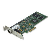
Ultrahigh Speed Fiber-Optic Reflective Memory with Interrupts
Brand:
GE
| Category:
PCI Card
| Size: 1.76 MB
Table of Contents
Table of Contents
3
List of Figures
5
List of Tables
6
Overview
8
Figure 1 Block Diagram of PCIE-5565PIORC
9
Figure 2 Typical Reflective Memory Network
10
1 Handling and Installation
15
Unpacking Procedures
15
Handling Precaution
15
Switch S1 and S2 Configuration
16
Before Installation Switch S1 and S2 Configuration
16
Table 1-1 Example Node ID Switch S2 RFM-5565
17
Table 1-2 Switch S1 Configuration RFM-5565
17
Figure 1-1 S1 and S2 Location PCIE-5565PIORC
18
Physical Installation
19
Figure 1-2 Installing the PCIE-5565PIORC
19
Front Panel Description
20
Figure 1-3 Low Profile and Standard Front Panels of the PCIE-5565PIORC
20
LED Description
21
Cable Configuration
21
Connector Specification (Singlemode and Multimode)
21
Table 1-3 LED Descriptions
21
Table 1-4 Cable Specifications for Multimode and Singlemode
21
Figure 1-4 LC Type Fiber-Optic Cable Connector
22
Figure 1-5 Example: Six Node Ring Connectivity PCIE-5565PIORC
22
2 Theory of Operation
23
Basic Operation
23
Front Bezel LED Indicators
23
RFM-5565 Register Sets
24
Reflective Memory RAM
24
Interrupt Circuits
25
Figure 2-1 Interrupt Circuitry Block Diagram
26
Network Interrupts
27
Redundant Transfer Mode of Operation
27
Rogue Packet Removal Operation
28
3 Programming
29
PCI Configuration Registers
30
Table 3-1 PCI Configuration Registers
30
Table 3-2 PCI Configuration ID Registers
30
Table 3-3 PCI Command Register
31
Table 3-4 PCI Status Register
32
Table 3-5 PCI Revision ID Register
32
Table 3-6 PCI Class Code Register
33
Table 3-7 PCI Cache Line Size Register
33
Table 3-8 PCI Latency Timer Register
33
Table 3-9 PCI Header Type Register
33
Table 3-10 PCI Built-In Self Test Register
34
Table 3-11 PCI Base Address Register 0 for Access to Local Configuration Registers
34
Table 3-12 PCI Base Address Register 1 for Access to Local Configuration Registers
35
Table 3-13 PCI Base Address Register 2 for Access to RFM Control and Status Registers
35
Table 3-14 PCI Base Address Register 3 for Access to Reflective Memory
36
Table 3-15 PCI Base Address Register 4
36
Table 3-16 PCI Base Address Register 5
36
Table 3-17 PCI Cardbus CIS Pointer Register
37
Table 3-18 PCI Subsystem Vendor ID Register
37
Table 3-19 PCI Subsystem ID Register
37
Table 3-20 PCI Expansion ROM Base Register
37
Table 3-21 PCI Capability Pointer Register
37
Table 3-22 PCI Interrupt Line
38
Table 3-23 PCI Interrupt Pin
38
Table 3-24 MSI Capability Structure
38
Table 3-25 Message Control Bit Definition
38
Table 3-26 Power Management Capability Structure
39
Table 3-27 Pcie Capability Structure
39
Table 3-28 Pcie Capabilities Register Bit Definition
39
Table 3-29 Device Capabilities Register Bit Definition
39
Table 3-30 Device Control Register Bit Definition
40
Table 3-31 Device Status Register Bit Definition
41
Table 3-32 Link Capabilities Register Bit Definition
41
Table 3-33 Link Control Register Bit Definition
41
Table 3-34 Link Status Register Bit Definition
42
Local Configuration Registers
43
Table 3-35 Local Configuration and DMA Control Registers
43
Table 3-36 Mode/Dma Arbitration Register
44
Table 3-37 Big/Little Endian Descriptor Register
44
Table 3-38 Interrupt Control and Status Register
45
Table 3-39 INTCSR Interrupt Enables
45
Table 3-40 INTCSR Interrupt Status
45
Table 3-41 PCI Core/Features Revision ID
46
Table 3-42 DMA Channel 0 Mode Register
46
Table 3-43 DMA Channel 0 PCI Address Register
46
Table 3-44 DMA Channel 0 Local Address Register
46
Table 3-45 DMA Channel 0 Transfer Size (Bytes) Register
47
Table 3-46 DMA Channel 0 Descriptor Pointer Register
47
Table 3-47 DMA Channel 0 Command/Status Register
47
Table 3-48 DMA Channel 0 PCI Dual Address Cycles Upper Address
48
Table 3-49 PCI PIO Direct Slave Local Address Range
48
Table 3-50 PCI PIO Direct Slave Local Base Address (Remap)
48
RFM Control and Status Registers
49
Table 3-51 Memory Map of the Local Control and Status Registers
49
Board ID Register
50
Board Revision Build Register
50
Board Revision Register
50
Local Control and Status Register 1
50
Node ID Register
50
Table 3-52 Local Control and Status Register 1
50
Local Interrupt Control Registers
54
Table 3-53 Local Interrupt Status Register
54
Network Target Data Register
57
Network Target Node Register
57
Table 3-54 Local Interrupt Enable Register
57
Interrupt 1 Sender Data FIFO
58
Interrupt 1 Sender ID FIFO
58
Network Interrupt Command Register
58
Table 3-55 Network Interrupt Command Register
58
Interrupt 2 Sender Data FIFO
59
Interrupt 2 Sender ID FIFO
59
Interrupt 3 Sender Data FIFO
59
Interrupt 3 Sender ID FIFO
59
Interrupt 4 Sender Data FIFO
59
Interrupt 4 Sender ID FIFO
59
Figure 3-1 Block Diagram of the Network Interrupt Reception Circuitry
60
Example of a Block DMA Operation for RFM-5565
61
Example of a Scatter-Gather DMA Operation for RFM-5565
62
Example of a PCI PIO Sliding Window Operation for RFM-5565
64
Example of Network Interrupt Handling
66
Setup
66
Servicing Network Interrupts
66
Maintenance
67
Compliance Information
68
Related Products
GE PCIE-5565PIORC*
GE PCVH485EK
GE PCP912
GE PCGB930
GE PCT7050
GE PCK916
GE PCHS920
GE Profile PCGB965
GE PCS940BMTS
GE PCB970
GE Categories
Refrigerator
Ranges
Microwave Oven
Air Conditioner
Dishwasher
More GE Manuals