
Related Manuals for Motorola CPV5000


Summary of Contents for Motorola CPV5000
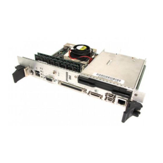
- Page 1 CPV5000 CompactPCI ® Single Board Computer Installation and Reference Guide CPV5000A/IH3...
- Page 2 While reasonable efforts have been made to assure the accuracy of this document, Motorola, Inc. assumes no liability resulting from any omissions in this document, or from the use of the information obtained therein. Motorola reserves the right to revise this document and to make changes from time to time in the content hereof without obligation of Motorola to notify any person of such revision or changes.
- Page 3 The CPV5000 Single Board Computer Installation and Reference Guide describes the installation, components, and configurations of the CPV5000. The document should be used by anyone who wants general as well as technical information about the CPV5000 Single Board Computer. ®...
- Page 4 The safety precautions listed below represent warnings of certain dangers of which Motorola is aware. You, as the user of the product, should follow these warnings and all other safety precautions necessary for the safe operation of the equipment in your operating environment.
- Page 5 All Motorola PWBs (printed wiring boards) are manufactured by UL-recognized manufacturers, with a flammability rating of 94V-0. This equipment generates, uses, and can radiate electro- magnetic energy. It may cause or be susceptible to electro- WARNING magnetic interference (EMI) if not installed and used in a cabinet with adequate EMI protection.
- Page 6 Lithium battery caution The board contains a lithium battery to power the clock and calendar circuitry. CAUTION: Danger of explosion if battery is incorrectly replaced. CAUTION Replace only with the same or equivalent type recommended by the equipment manufacturer. Dispose of used batteries according to the manufacturer’s instructions.
-
Page 7: Table Of Contents
Special functions ....................1-5 Additional information resources................. 1-5 Chapter 2 Getting Started Antistatic precautions................... 2-1 Before installing the CPV5000 ................2-2 Installation instructions ..................2-3 Powering up the CPV5000................... 2-5 Coin Battery ......................2-5 Front panel ......................2-6 Chapter 3 Connectors and Components on the CPV5000 Components ...................... - Page 8 SCSI, X3T10 SPI/single ended levels ...........3-10 VGA Video, VGA levels...............3-11 J5 Signal Descriptions..................3-13 General....................3-13 Miscellaneous Signals ................3-13 Keyboard/Auxiliary Device, TTL levels ..........3-13 Universal Serial Bus (USB) (0 & 1), USB levels........3-13 Parallel LPT Port, TTL levels (some signals are redefined when used in EPP/ECP modes)...............3-14 Serial COM Ports (a &...
- Page 9 USB ........................4-15 Keyboard/mouse interface ................. 4-16 Ethernet ......................4-16 DMA channels ....................4-16 Interrupts ......................4-17 FPGA Access, Watchdog and ENUM registers ..........4-18 Port offset 0Bh: board status and watchdog strobe....... 4-18 I/O port offset 0Dh: FPGA register index port ........4-19 I/O port offset 0Fh: FPGA register data port ........
- Page 10 POST checkpoint codes ..................6-9 Uncompressed initialization codes..............6-9 Runtime checkpoint codes ................6-10 Bus checkpoint codes ...................6-15 Additional bus checkpoints ................6-17 Chapter 7 WinBIOS Setup Starting WinBIOS Setup..................7-1 WinBIOS Setup features..................7-1 Icon-based user interface................7-1 Automatic option selection................7-1 Help screens ....................7-2 Automatic WinBIOS Setup option selection..........7-2 Point and click interface.................7-2 Mouse support ....................7-2 Memory test tick sound ..................7-3...
- Page 11 Mouse support..................7-13 Primary display ..................7-13 Password check ..................7-14 Internal cache ..................7-14 External cache ..................7-14 System BIOS shadow cacheable............7-15 Chipset setup ....................7-16 Memory hole ..................7-16 IRQ12/M mouse function ..............7-16 DRAM speed ..................7-16 Refresh rate ...................
- Page 12 Plug and play aware OS.................7-22 PCI latency timer (in PCI clocks)............7-22 PCI VGA palette snoop .................7-22 PCI IDE bus master ................7-22 Offboard PCI IDE board................7-22 DMA channels ..................7-23 ISA/PCI IRQ allocation.................7-23 Reserved memory size................7-24 Reserved memory address ..............7-24 Peripheral setup ....................7-24 Onboard FDC..................7-24 Onboard serial port 1/COM 1 ..............7-24 Onboard serial port 2/COM 2 ..............7-25...
- Page 13 Figure 1-1. Block diagram ................. 1-4 Figure 2-1. Installing the CPV5000 ..............2-4 Figure 2-2. Front panel connectors and LEDs ........... 2-6 Figure 3-1. Location of main components on the CPV5000......3-2 Figure 4-1. SCSI termination ................4-12 Tables Table 1-1. Input/Output interfaces ............... 1-3 Table 1-2.
- Page 14 Table 4-3. I/O addresses..................4-5 Table 4-4. Memory address ..................4-6 Table 4-5. Standard video modes................4-7 Table 4-6. Extended video modes.................4-8 Table 4-7. On-board drive options ..............4-14 Table 4-8. DMA channels ...................4-17 Table 4-9. Interrupts....................4-18 Table 4-10. I/O offset 0Bh (write) ..............4-19 Table 4-11.
- Page 15 Table 7-9. External cache .................. 7-15 Table 7-10. System BIOS shadow cacheable............. 7-16 Table 7-11. Parallel port mode................7-26...
-
Page 17: About This Book: Changes Between Ih2 And Ih3
3.3V power supply as the board is powered up can cause the CPV5000 to inaccurately report the CPU clock speed. In order to prevent this, it is necessary that the 5V power supply ramp up at the same time (or before) the 3.3V supply does. -
Page 18: Additional Features
CPV5000 Single Board Computer Overview Additional features The CPV5000 also supports these features: • Parallel port interface (available through rear I/O and front panel on a Micro-D connector) • Two high speed 16650 serial ports (available through rear I/O and front panel on a stacked Micro-D connector) •... -
Page 19: Input/Output Interfaces
Refer to Table 1-1 for brief descriptions of the input/output interfaces on the CPV5000. Note When the identical function is available through the CPV5000’s front panel and the rear transition module, you can use either the front or the rear, not both. Table 1-1. Input/Output interfaces Function... -
Page 20: Figure 1-1. Block Diagram
CPV5000 Single Board Computer Overview Video KBD/Mouse LPT 1 COM 2 COM 1 Ethernet SCSI RJ45 Mini Dsub Dsub Micro D Micro D Micro D LM78 System Monitor On-board IDE Hard Drive On-board or Flash Floppy Ultra South Ethernet Ultra... -
Page 21: Special Functions
Special functions Special functions The CPV5000 uses three functions that are designed for use in certain applications. These are: • Watchdog Timer The watchdog timer is a count down timer. When the counter reaches zero, it can set a flag in a register, optionally assert IOCHK (NMI), and optionally perform an SBC reset. - Page 22 CPV5000 Single Board Computer Overview...
-
Page 23: Antistatic Precautions
PICMG CompactPCI compliant CompactPCI backplane. Antistatic precautions Take care when handling the CPV5000. The CPV5000 and its active components are sensitive to electrostatic discharge (ESD), and can easily be damaged. Motorola recommends that you use an antistatic Caution wrist strap when handling the CPV5000 and associated components. -
Page 24: Before Installing The Cpv5000
Getting Started Before installing the CPV5000 After removing the CPV5000 from its packaging: • Check for obvious physical damage. • Verify that the coin cell battery is in its holder and inserted correctly. • Verify that the CPU fan is connected. -
Page 25: Installation Instructions
3. Remove any filler panel (or existing CPU board) that might fill that slot. 4. Install the top and bottom edge of the CPV5000 in the guides of the chassis. 5. Ensure that the levers of the two injector/ejectors are in the inward position. -
Page 26: Figure 2-1. Installing The Cpv5000
Getting Started 21659803 Figure 2-1. Installing the CPV5000... -
Page 27: Powering Up The Cpv5000
• On powering up, the CPV5000 displays the AMIBIOS revision and then runs a memory test. If thekey is pressed during the memory test, the CPV5000 will enter the Basic Input/Output System (BIOS) setup after completing the memory test. -
Page 28: Front Panel
Getting Started Front panel The CPV5000’s front panel has connectors for keyboard/mouse, SCSI, video, parallel printer, COM1/2, and ethernet. Indicator lights on the front panel display power, hard disk activity, watchdog alarm, and speaker status. Keyboard/Mouse CompactPCI Indicator lights Reset... -
Page 29: Components
3Connectors and Components on the CPV5000 Components The CPV5000 single board computer carries components on both sides. Figure 3-1 shows the location of the connectors and headers. Table 3-1. Major chip functions Reference Description Manufacturer Part Number Ethernet Intel S82557... -
Page 30: Figure 3-1. Location Of Main Components On The Cpv5000
Connectors and Components on the CPV5000 FLOPPY FPGA BIOS CPCI BRIDGE CACHE VIDEO ETHERNET NORTH SOUTH BATTERY BRIDGE BRIDGE CACHE MEMORY SCSI SIMMs ULTRA I/O BANK 1 BANK 0 Figure 3-1. Location of main components on the CPV5000... -
Page 31: Connecting To And Configuring Headers
Only qualified, experienced electronics personnel should access the interior of a chassis. The components of the CPV5000 are sensitive to static discharge. While out of the unit, the CPV5000 should be placed on a static- dissipative surface or into a static-shielding bag. Caution... -
Page 32: Cpu Speed Settings
Connectors and Components on the CPV5000 CPU speed settings Table 3-2 describes the possible jumper settings for different speed CPUs. Install a shorting block across two pins on each of the four speed configuration jumpers to configure any given speed. -
Page 33: Cpu Voltage Settings
CPU Voltage Settings CPU Voltage Settings J30 has been added to the CPV5000 with the introduction of the AMD processor, because Intel and AMD processors run on different core voltages. If you are using an Intel processor, then you should jumper J30. If you are using an AMD processor, then leave the jumper off. -
Page 34: Usb Configuration
Connectors and Components on the CPV5000 USB configuration The USB configuration jumper is a two by four jumper block. A four position shorting block is installed to select the USB routing. To maintain signal integrity, the USB signals can be routed to the rear connector. If rear connector routing is selected, no USB devices can be installed on the front connector. -
Page 35: Rear I/O Connectors
External power (+12V) J3, J4 4-pin latching connector Fan power and Tach inputs On-board connectors Table 3-7 specifies the connectors that are available to support devices on the CPV5000. Table 3-7. On-board connectors Location Type Description 44 (2x22) pin shrouded header... -
Page 36: Connectors J4 And J5
Connectors and Components on the CPV5000 Connectors J4 and J5 The following table describes the common product pin-out for the CompactPCI user I/O connector as seen from the rear of the backplane. This signal arrangement is proposed for bringing out the I/O signals common to 6U CompactPCI processor boards based on the ”Win-tel”... -
Page 37: J4 Signal Descriptions
SSDA - LM78 I2C serial data I/O SSCL - LM78 I2C serial clock input Ethernet, RS422 levels ERX+/- - differential receive line pair (CPV5000 requires transformer to connect to network) ETX+/- - differential transmit line pair (CPV5000 requires transformer to connect to... -
Page 38: Scsi, X3T10 Spi/Single Ended Levels
GND/NDET* - narrow detect, may be pulled low to indicate that bits[7:0] are connected (GND on CPV5000) GND/WDET* - wide detect, may be pulled low to indicate that bits[15:8] are connected (GND on CPV5000) GND/SLED* - SCSI active LED signal, TTL active low (GND on CPV5000) 3-10... -
Page 39: Vga Video, Vga Levels
Connectors J4 and J5 VGA Video, VGA levels BLUE - blue signal HSYNC - horizontal sync GREEN - green signal RED - red signal VSYNC - vertical sync DDCDAT - VESA Display Data Channel data (I2C) DDCCLK - VESA Display Data Channel clock (I2C) 3-11... -
Page 40: Table 3-9. J5 Connector Pin Assignments
Connectors and Components on the CPV5000 Table 3-9. J5 connector pin assignments Pin # Row F Row E Row D Row C Row B Row A Row Z SPKR*OC DIAG*OC PBRESET* AUXCLK AUXDAT KBDCLK KBDDAT SMBCLK SMBALERT* SMDATA UDATA0- UDATA0+... -
Page 41: J5 Signal Descriptions
(pulled up, filtered, and debounced on host card) RESET* system reset output, TTL totem-pole [on CPV5000, asserted only when 5V power is out of tolerance and upon manual reset (push-button) assertion] Keyboard/Auxiliary Device, TTL levels... -
Page 42: Parallel Lpt Port, Ttl Levels (Some Signals Are Redefined When Used In Epp/Ecp Modes)
Connectors and Components on the CPV5000 Parallel LPT Port, TTL levels (some signals are redefined when used in EPP/ECP modes) ACK* pulsed by peripheral to acknowledge data sent BUSY indicates that the printer cannot accept more data ERR* peripheral detected an error... -
Page 43: Eidea (Ata-2), Ttl Levels
Connectors J4 and J5 HDSEL* selects top or bottom side head INDEX* indicates the beginning of a track MTR[1:0]* motor enables RDATA* read data STEP* step head in or out TR0* indicates that head is positioned above track 00 WDATA* write data to drive WGATE* enables head write circuitry of drive... -
Page 44: Parallel Port Connector
The parallel port is normally used for connecting a cable to a printer. This port is available as a 25-pin micro-D connector on the front panel of the CPV5000 front panel or as a 26-pin header and 25-pin standard D connector on the rear panel of the CPV5000 transition module. -
Page 45: Eide Hard Drive Connectors
Note The red stripe on the 40-pin EIDE ribbon cable should be near pins 1 and 2 on the 40-pin connector. The CPV5000 and EIDE hard drive(s) will not work correctly if the cable is plugged in backwards. EIDE cables should be no more than 18 inches (46 cm) long. - Page 46 Connectors and Components on the CPV5000 Table 3-11. EIDE connector pin assignments (Continued) Signal Signal Description Signal Signal Description Number Mnemonic Number Mnemonic DD14 Data Bus Bit 14 CS3- Chip select drive 1, also command register block select Data Bus Bit 0...
-
Page 47: Floppy Connector
Floppy connector Floppy connector One diskette drive can be attached to the CPV5000 via the 26-pin header (J20) for on-board mounting. Alternatively, two diskette drives can be remotely attached to the CPV5000 via the 34-pin header on the transition module. Note that the floppy disk drive controller cable should be no more than three feet (91 cm) long. - Page 48 Connectors and Components on the CPV5000 Table 3-12. Floppy connector pin assignments (Continued) Signal Signal Description Number Mnemonic TR0- Indicates head of FDD is at track 0 Ground WPROT- Indicates a disk is write-protected Ground RDATA- Raw red data from disk drive...
-
Page 49: Ps/2 Keyboard/Mouse Connector
PS/2 keyboard/mouse connector The PS/2 connector is a 6-pin connector mounted on the end bracket of the CPV5000. The PS/2 Y adapter cable supplied attaches to this connector. The CPV5000 transition module has two connectors for the keyboard and mouse. -
Page 50: Serial Ports Com1 And Com2 Connectors
Serial ports allow you to connect serial devices (a serial mouse, serial printers) to the CPV5000 via appropriate serial cables. COM1 and COM2 are 9-pin micro-D connectors located on the CPV5000 front panel and regular D connectors on the transition module. -
Page 51: Fan Power Connector
Signal Number Tach Ground +12V USB ports 1 and 2 USB ports 1 and 2 are available through the CPV5000’s front panel or the transition module’s rear panel. Table 3-16. USB ports pin assignments Signal Mnemonic Signal Description Number Current limited USB power... -
Page 52: Ethernet Connector
Connectors and Components on the CPV5000 Ethernet connector An Ethernet RJ45 connector is available through the CPV5000’s front panel or the transition module’s rear panel. Table 3-17. Ethernet connector pin assignments Signal Signal Description Number Mnemonic Transmit data Transmit data return... -
Page 53: Scsi Connector
SCSI connector SCSI connector A SCSI connector is available through the CPV5000’s front panel or the transition module’s rear panel. For information on SCSI termination, see Ultra SCSI controller, page 4-11. Table 3-18. 68-pin SCSI-3 connector pin assignments Signal Signal Name... - Page 54 Connectors and Components on the CPV5000 Table 3-18. 68-pin SCSI-3 connector pin assignments (Continued) Signal Signal Name Signal Signal Description Number Mnemonic Number Mnemonic Ground Command/data Ground REQ- Request Ground Input/output Ground SCSI data bus (bit 8) Ground SCSI data bus (bit 9)
-
Page 55: Video Connector
Video connector Video connector Table 3-19. Video connector pin assignments Signal Signal Description Number Mnemonic Red signal GREEN Green signal BLUE Blue signal Not connected DACVSS Video return DACVSS Video return DACVSS Video return DACVSS Video return Not connected DACVSS Video return Not connected DDCDAT... -
Page 56: Reset Switch
Connectors and Components on the CPV5000 Reset switch Table 3-20. Reset switch pin assignments Signal Mnemonic Number Ground FR RSET- 3-28... -
Page 57: Peripheral Component Interconnect (Pci) Local Bus
4Functional Description The CPV5000 is designed to operate with a Pentium or a K-6 microprocessor. It supports both read and write burst mode bus cycles and includes an on-chip 16 KB cache that is split into 8 KB code and data caches employing a write- back policy. -
Page 58: Pci Device Mapping And Routing
Functional Description PCI device mapping and routing Table 4-1 lists all PCI components with ID codes. Table 4-1. PCI components Device Name Manufacturer Part # Device ID Vendor BIOS Extension Host Bridge TXC Intel 82439HX 0x1250 0x8086 ISA Bridge PIIX3 Intel 82371 0x7000... -
Page 59: Pci Routing Table
Watchdog timer PCI routing table Table 4-2 shows PCI interrupt routing. Table 4-2. PCI interrupt routing Description Bus # IDSel Device # Req/Gnt INTA INTB INTC INTD Host Bridge 0x00 PIIX3 AD18 0x07 PHOLD Ethernet AD31 0x14 PIRQB Video AD30 0x13 PIRQC Bridge 1... -
Page 60: I/O Address Map
Functional Description • Set a flag in a register in ISA I/O memory map • Item 2 + Assert a selectable ISA interrupt • Item 2 + Assert NMI followed by a system reset. The watchdog timer is programmable via registers in the ISA I/O memory map. -
Page 61: Table 4-3. I/O Addresses
I/O address map Table 4-3. I/O addresses Address Function 0000-000F DMA controller 1 0020-0021 Interrupt controller 1 0040-0043 Counter timer 0060-0064 Keyboard, NMI, speaker 0070-0071 Real time clock/NMI mask 0050-0057 LM78 System monitor (opt) 0058-005F WatchDog timer, ENUM (opt) 0080-009F DMA page register, POST checkpoint 00A0-00BF Interrupt controller 2... -
Page 62: Memory Address Mapping
Functional Description Table 4-3. I/O addresses (Continued) Address Function 0678-067A Parallel port 2 (opt) 0778-077A Parallel port 1 (opt) 07BC-07BE Parallel port 3 (opt) 0CF8-0Cff PCI configuration 1. The WatchDog timer and LM78 are normally disabled but may be relocated and enabled via PCI configuration. -
Page 63: Video Controller
• No external video installed: on board video enabled • External video installed: on board video disabled The CPV5000 has a Cirrus Logic 64-bit VisualMedia Accelerator chip. Table 4-5 and Table 4-6 list the chip’s video modes. Table 4-5. -
Page 64: Table 4-6. Extended Video Modes
Functional Description Table 4-6. Extended video modes Mode# VESA # of Colors Char. Char. Screen Display Horiz. Vert. Mode # xRow Cell Format Mode Clock Freq Freq. Hz 16/256K 132x25 8x16 1056x400 Text 41.5 31.5 16/256K 132x43 1056x350 Text 41.5 31.5 55[7] 16/256K... - Page 65 Video controller Table 4-6. Extended video modes (Continued) Mode# VESA # of Colors Char. Char. Screen Display Horiz. Vert. Mode # xRow Cell Format Mode Clock Freq Freq. Hz 32K[3] 640x480 Graphics 31.5 37.5 32K[3] 800x600 Graphics 35.2 32K[3] 800x600 Graphics 37.8 32K[3]...
- Page 66 Functional Description [7] Mode 55 will use a 16 dot high font, with the bottom two lines truncated, in the absence of the 8x14 font TSR (TSRFONT). The characters “g,” “j,” “p,” “q,” “y,” and “Ø” are truncated using a middle and bottom line algorithm to avoid truncation of descenders.
-
Page 67: Ultra Scsi Controller
Ultra SCSI controller Ultra SCSI controller The Adaptec 7880 chip is used for on-board support for Ultra SCSI. The user can enable or disable this feature through the BIOS Setup screen. Connection to the SCSI device is available on the front panel and the rear I/O transition module via a 68-pin, high-density connector. -
Page 68: Figure 4-1. Scsi Termination
Functional Description Figure 4-1. SCSI termination 4-12... - Page 69 The last device on the cable provides termination for these signals. If a wide device is plugged into the CPV5000’s 68-pin connector, pin 1 will be grounded, and all three terminators will be turned off. In this case, a wide device must be connected at the end of the cable.
-
Page 70: Eide Interface
Functional Description EIDE interface The EIDE interface supports primary and secondary both interfaced via the rear I/O transition module. The primary EIDE channel is available for the connection of on-board devices through an on-board height density connector. The IDE interface supports ATAPI modes 0 to 4. Each IDE interface supports two IDE devices (master and slave). -
Page 71: Parallel Port
I/O transition module, or a 25-pin micro-D connector on the front panel. Serial ports The CPV5000 supports two serial ports. The ports support 16550 operation. The serial interface connector is a 9-pin D style connector available on the rear I/O transition module, or 9-pin micro-D connectors available on the front panel. -
Page 72: Keyboard/Mouse Interface
Functional Description Keyboard/mouse interface The keyboard and mouse is supported by a single PS/2 connector on the front panel and separate PS/2 style connectors on the rear I/O transition module. The front I/O keyboard/mouse connector utilizes a standard splitter cable to connect to a mouse and keyboard. -
Page 73: Interrupts
Interrupts Interrupts Table 4-9. Interrupts Channel Function Reports parity / System errors System management System timer Keyboard Cascade for IRQ 8-15 COM 2/serial port 2 COM 1/serial port 1 Parallel port 2 Floppy controller Parallel port 1 Real time clock Software redirect to IRQ2 Reserved Reserved / special features... -
Page 74: Fpga Access, Watchdog And Enum Registers
Functional Description FPGA Access, Watchdog and ENUM registers The LM78 and the FPGA’s watchdog timer is addressed through the Programmable Chip Select in the South Bridge. The PCS is set to a default address of 0050h by the BIOS. This can be changed at any time by an application program if this becomes a conflict. -
Page 75: I/O Port Offset 0Dh: Fpga Register Index Port
FPGA Access, Watchdog and ENUM registers I/O port offset 0Dh: FPGA register index port A Field Programmable Gate Array (FPGA) on the CPV5000 contains the watchdog timer and miscellaneous registers. The value written to the index port selects which FPGA register is accessible from port offset 00Fh. Index-0 is selected at reset and is selected after any output to the FPGA data port offset 0Fh. -
Page 76: I/O Port Offset 0Fh: Fpga Register Data Port
Functional Description I/O port offset 0Fh: FPGA register data port All communication of data from the CPV5000 is implemented through the FPGA register data port. The function of each bit is dependent on the data in the I/O port offset 0Dh: FPGA register index port. -
Page 77: Bit 7 - Clear Watchdog Bit
Set the watchdog flag when timer counts to zeroes Set the watchdog flag and assert IOCHRDY when the timer counts to zeroes Set the watchdog flag and assert IOCHRDY and RESET the CPV5000 when the timer counts to zeroes 4-21... -
Page 78: Bits 2-0 Watchdog Timer Delay
Functional Description Bits 2-0 watchdog timer delay Bits 2 to 0 control the delay of the watchdog timer until the function bits 4 to 3 are activated. Table 4-17. Watchdog timer delay Data Watchdog count down delay 17.8 milliseconds 71.1 milliseconds 284 milliseconds 1.14 seconds 4.55 seconds... -
Page 79: Enum Storage Register: Fpga Index - 12H
FPGA Access, Watchdog and ENUM registers ENUM storage register: FPGA index - 12h The ENUM storage register is used to store a byte of information for hot swap enabled systems. A byte of information can be stored and read back at this location. Table 4-19. - Page 80 Functional Description 4-24...
-
Page 81: Installing Options
64-bit wide data path and eight parity bits. Memory timing requires 60 ns or 70 ns fast page mode devices. The CPV5000 supports up to 256 MB of on-board FPM memory or up to 256 MB of on-board EDO memory in various configurations. EDO memory is often used for improved performance with or without secondary cache. -
Page 82: Table 5-1. Memory Configurations
Installing Options Table 5-1. Memory configurations Total System SIMM J6, J7 (Bank 0) SIMM J8, J9 (Bank 1) Memory SIMM Type (Amount) SIMM Type (Amount) 8 MB 1M X 36 (4 MB) EMPTY 16 MB 1M X 36 (4 MB) 1M X 36 (4 MB) 24 MB 1M X 36 (4 MB) -
Page 83: Installing Dram Simms
3. Insert the SIMM at a 45 degree angle. 4. Gently push the SIMM into an upright position until it locks into place. 5. Install the CPV5000 in the chassis and connect the power cords. Apply power to the chassis. -
Page 84: Upgrading The Cpu
Remove the CPV5000 from the chassis. 2. Locate the CPU socket. 3. Place the CPV5000 on a flat surface and remove the fan and heat sink by disconnecting the cable, and then releasing the retaining clip. 4. Release the (ZIF) lever by first pushing the lever away from the socket and then lifting up. -
Page 85: Table 5-2. Cpu Speed Settings
8. Connect the fan power cable. 9. Check the CPU speed jumper settings. Table 5-2. CPU speed settings CPU Speed 166 Mhz 200 Mhz 233 Mhz 266 Mhz 300 Mhz 10. Install the CPV5000 in the chassis and connect the power cords. -
Page 86: Removing And Replacing The Battery
5. Install the CPV5000 in the chassis and connect the power cords. 6. When the CPV5000 powers on, the optimal BIOS setting will have to be loaded. For information on how to load the BIOS settings, see Chapter 7, Starting... -
Page 87: Installing The On-Board Disk Drives
Removing and Replacing the Battery Installing the on-board disk drives The CPV5000 has an optional, on-board EIDE drive and a floppy drive. Installation instructions Use the following procedure to install the on-board disk and floppy drives. A number one Phillips screwdriver is needed for this procedure. - Page 88 3. If installing a floppy drive, attach one end of the cable to its connector on the CPV5000. To attach the cable, push up on each end of the plastic connector. The connector releases so that the cable can be inserted in the connector.
- Page 89 5. If you are installing a hard drive, attach the cable to the drive and the IDE connector on the CPV5000. 6. Attach the drive carrier to the CPV5000 using two screws. 2173 9803...
- Page 90 7. Attach the remaining end of the floppy cable. Push up on the tabs on the connector and insert the floppy cable. Push down on the tabs to secure the cable. 2171 9803 8. Install the CPV5000 in the chassis and connect the power cords. 5-10...
-
Page 91: Power On Self-Tests
Power On Self-Tests This chapter contains information to help you troubleshoot the system. It describes error reporting methods and suggests appropriate solutions to various problems. American Megatrends Inc. Basic Input/Output System ® (AMIBIOS) provides all IBM standard Power-On Self Test (POST) routines as well as enhanced AMIBIOS POST routines. -
Page 92: Bios Error Reporting
Power On Self-Tests BIOS error reporting BIOS errors are reported by a series of beep sounds or when an error message is displayed to the screen. Refer to Table 6-1 for BIOS error reporting information. This section contains information on the following: •... -
Page 93: Beep Codes
BIOS error reporting Beep codes Fatal errors, which halt the boot process, are communicated through a series of audible beeps. If AMIBIOS POST can initialize the system video display, it displays the error message on the screen. Displayed error messages, in most cases, allow the system to continue to boot. -
Page 94: Amibios Displayed Error Messages
Power On Self-Tests AMIBIOS displayed error messages The following section describes the operation of the CPV5000 when the BIOS detects an error during power up of the CPV5000. The explanation assumes that a copy of AMI diagnostics is available to assist with debug of the problem. - Page 95 AMIBIOS displayed error messages Table 6-3. AMIBIOS error messages (Continued) Message Explanation CMOS display type The video type in CMOS RAM does not match the type detected. Run mismatch WINBIOS Setup. CMOS memory size The amount of memory found by AMIBIOS is different than the amount mismatch in CMOS RAM.
- Page 96 XXXX is the hex address where the error occurred. Run AMIDiag to find and correct memory problems. On board parity error Parity error in CPV5000 DRAM memory. The format is: ON BOARD PARITY ERROR ADDR = (XXXX) XXXX is the hex address where the error occurred. Run AMIDiag to find and correct memory problems.
-
Page 97: Post Memory Test
POST memory test POST memory test Normally, the only visible POST routine is the memory test. When the system is powered on the following screen appears: AMIBIOS (C) 1995 American Megatrends Inc. KB OK XXXXX Hitif you want to run SETUP (C) American Megatrends Inc. -
Page 98: Bios Revision
BIOS revision The monitor displays this message before displaying the AMI configuration screen. The actual BIOS revision should be quoted in all communication with Motorola. AMIBIOS configuration screen When the POST routines complete successfully, AMIBIOS displays a screen similar to the following: AMIBIOS System Configuration (C) Copyright 1985-95 American Megatrends Inc. -
Page 99: Post Checkpoint Codes
POST checkpoint codes POST checkpoint codes When AMIBIOS performs the POST routine, it writes diagnostic codes, that is checkpoint codes, to I/O port 0080h. If the computer cannot complete the boot process, diagnostic equipment can be attached to the computer to read I/O port 0080h. -
Page 100: Runtime Checkpoint Codes
Power On Self-Tests Runtime checkpoint codes The runtime checkpoint codes are listed in order of execution in Table 6-6. These codes are uncompressed in F0000h shadow RAM. Table 6-6. Runtime checkpoint codes Checkpoint Description code The NMI is disabled. Next, checking for a soft reset or a power on condition. The BIOS stack has been built. - Page 101 POST checkpoint codes Table 6-6. Runtime checkpoint codes (Continued) Checkpoint Description code The configuration required before interrupt vector initialization has completed. Interrupt vector initialization is about to begin. Interrupt vector initialization is complete. Clearing the password if the POST DIAG switch is on.
- Page 102 Power On Self-Tests Table 6-6. Runtime checkpoint codes (Continued) Checkpoint Description code The descriptor tables are prepared. Entering protected mode for the memory test next. Entered protected mode. Enabling interrupts for diagnostics mode next. Interrupts enabled if the diagnostics switch is on. Initializing data to check memory wraparound at 0:0 next.
- Page 103 POST checkpoint codes Table 6-6. Runtime checkpoint codes (Continued) Checkpoint Description code The memory size information and the CPU registers are saved. Entering real mode next. Shutdown was successful. The CPU is in real mode. Disabling the Gate A20 line, parity, and the NMI next.
- Page 104 Power On Self-Tests Table 6-6. Runtime checkpoint codes (Continued) Checkpoint Description code The password was checked. Performing any required programming before WINBIOS Setup next. The programming before WINBIOS Setup has completed. Uncompressing the WINBIOS Setup code and executing the AMIBIOS Setup or WINBIOS Setup utility next.
-
Page 105: Bus Checkpoint Codes
POST checkpoint codes Table 6-6. Runtime checkpoint codes (Continued) Checkpoint Description code Coprocessor initialized. Performing any required initialization after the coprocessor test next. Initialization after the coprocessor test completes. Checking the extended keyboard, keyboard ID, and Num Lock key next. Issuing the keyboard ID command next. Displaying any soft errors next. -
Page 106: Table 6-7. Bus Checkpoint Codes
Power On Self-Tests Table 6-7. Bus checkpoint codes Checkpoint Description code Initializing the different bus system, static, and output devices, if present. Initialized bus input, IPL, and general devices, if present. Displaying bus initialization error messages, if any. Initializing bus adaptor ROMs from C8000h through D8000h. 6-16... -
Page 107: Additional Bus Checkpoints
POST checkpoint codes Additional bus checkpoints While control is in the bus routines, additional checkpoints are output to I/O port address 0080h as data to identify the routines being executed. There are two byte checkpoints and these are: • The low byte - The low byte of the checkpoint is the system BIOS checkpoint where control is passed to the different bus routines. - Page 108 Power On Self-Tests 6-18...
-
Page 109: Starting Winbios Setup
7WinBIOS Setup This chapter contains information on WinBIOS Setup. WinBIOS Setup configures system information that is stored in CMOS RAM. Starting WinBIOS Setup When the Power-On Self Test (POST) executes, the following message appears on the screen: Hitif you want to run SETUP You must then press... -
Page 110: Help Screens
WinBIOS Setup Help screens WinBIOS Setup provides Help screens for Advanced Setup, Chipset Setup, Power Management Setup, and Peripheral Setup. Help on mouse and keyboard is also available. Choose Help by pressing. Automatic WinBIOS Setup option selection If selecting a certain setting for one WinBIOS Setup option determines the settings for one or more other WinBIOS Setup options, AMIBIOS automatically assigns the dependent settings and does not permit the end user to modify these settings unless the setting for the parent option is changed. -
Page 111: Memory Test Tick Sound
WinBIOS Setup features • Logitech C-series-compatible mouse that uses the MM protocol Memory test tick sound AMIBIOS permits the end user to pressor during the memory test to disable the ticking sound and bypass the memory test. The memory click test will only be heard when the Quick boot is disabled. -
Page 112: Using The Keyboard With Winbios Setup
WinBIOS Setup Using the keyboard with WinBIOS Setup WinBIOS Setup has a built-in keyboard driver that uses simple keystroke combinations. Refer to Table 7-1 for keystroke combination information. Table 7-1. Keystroke combinations Keystroke FunctionMove to the next window or field →, ←, ↑, ↓... -
Page 113: Winbios Setup Main Menu
WinBIOS Setup main menu WinBIOS Setup main menu The WinBIOS Setup main menu is organized into four windows. Each window corresponds to a section in this chapter. Each section contains several icons. Clicking on each icon activates a specific function. The WinBIOS Setup icons and functions are described in this chapter. -
Page 114: Winbios Setup Types
WinBIOS Setup WinBIOS Setup types WinBIOS Setup can have up to six separate screens. Different types of system configuration parameters are set on each screen. Refer to Table 7-3 for WinBIOS Setup information. Table 7-3. WinBIOS Setup Type Description Turn to Standard Setup Set the time and date. -
Page 115: Pri Master Pri Slave Sec Master Sec Slave
WinBIOS Setup types Pri Master Pri Slave Sec Master Sec Slave Choose these icons to configure the hard disk drive named in the option. When you click on an icon, the following parameters are listed: • Type • LBA/Large Mode •... -
Page 116: User-Defined Drive
WinBIOS Setup User-defined drive If you are configuring a SCSI drive or an MFM, RLL, ARLL, or ESDI drive with drive parameters that do not match drive types 1-46, you can select the User in the Type field. You must then enter the drive parameters on the screen that appear. -
Page 117: Configuring Ide Drives
WinBIOS Setup types Configuring IDE drives If the hard disk drive to be configured is an IDE drive, select the appropriate drive icon (Pri Master, Pri Slave, Sec Master, or Sec Slave). Select the IDE Detect icon to automatically detect all drive parameters. AMIBIOS automatically detects the IDE drive parameters (including ATAPI CD-ROM drives) and displays them. -
Page 118: Configuring A Cd-Rom Drive
WinBIOS Setup Click on PIO Mode to select the IDE Programmed I/O mode. PIO programming also works with ATAPI CD-ROM drives. The settings are Auto, 0, 1, 2, 3, 4, or 5. Click on Auto to allow AMIBIOS to automatically find the PIO mode that the IDE drive being configured uses. - Page 119 WinBIOS Setup types Table 7-6. Hard drive type information (Continued) Type Cylinders Heads Write Landing Sector Capacity Zone 20 MB 41 MB 65535 57 MB 1024 1023 60 MB 30 MB 43 MB 30 MB 10 MB 54 MB 65535 69 MB 44 MB 65535...
-
Page 120: Advanced Setup
WinBIOS Setup Table 7-6. Hard drive type information (Continued) Type Cylinders Heads Write Landing Sector Capacity Zone 48 MB 65535 69 MB 65535 114 MB 1224 65535 1223 152 MB Advanced Setup Advanced Setup options are displayed by choosing the advanced icon from the WINBIOS Setup main menu. -
Page 121: Bootup Sequence
WinBIOS Setup types BootUp sequence This option sets the sequence of boot drives that the AMIBIOS attempts to boot from after AMIBIOS POST completes. The first boot device can be any of the following: IDE floppy, floptical, CD ROM, SCSI, or network. The second boot device can be any of the following: Disabled, IDE loptical, or CD ROM. -
Page 122: Password Check
WinBIOS Setup Password check This option enables password checking every time the computer is powered on or every time WINBIOS Setup is executed. If Always is chosen, a user password prompt appears every time the computer is turned on. If Setup is chosen, the password prompt appears if WINBIOS is executed. -
Page 123: System Bios Shadow Cacheable
WinBIOS Setup types System BIOS shadow cacheable When this option is set to Enabled, the contents of the F0000h system memory segment can be read from or written to L2 secondary cache memory. The contents of the F0000h memory segment are always copied from the BIOS ROM to system RAM for faster execution. -
Page 124: Chipset Setup
The settings are Disabled or Enabled. DRAM speed Specify the RAS access speed of the SIMMs installed in the CPV5000 as system memory. The settings are 60 ns or 70 ns. The default is 70 ns. Manual setting is not supported. -
Page 125: Read Burst Timing
WinBIOS Setup types Read burst timing This option is only available in manual DRAM setup. This option controls the read burst timings. The options are x444, x333 and x222. The slowest option is x444. The option x222 is only available for EDO DRAM. Write burst timing This option is only available in manual DRAM setup. -
Page 126: Na Disable (Nad) For External Cache
CPU pipelining. This option should be enabled. If this option is disabled, the CPU will not enable memory read/write pipeline modes, this will slow CPV5000 memory performance significantly. Extended cachebility This option should be enabled if the total system DRAM is greater than 64 MB. -
Page 127: Bad Parity On Uncorrectable Err
This controls the output driver of the SERR# pin. This should be set to Open Drain when used in a PCI system. SERR# duration mode This should be set to Pulse (NMI) for correct CPV5000 operation. Power Management Setup Power Management Setup options are displayed by choosing the power management icon from the WINBIOS Setup main menu. -
Page 128: Video Power Down Mode
WinBIOS Setup Video power down mode This option specifies the power management state that the video subsystem enters after the specified period of display inactivity has expired. The settings are: Disabled, Standby, or Suspend. Hard disk power down mode This option specifies the power management state that the hard disk drive enters after the specified period of display inactivity has expired. -
Page 129: Slow Clock Ratio
WinBIOS Setup types Slow clock ratio This option specifies the speed at which the system clock runs in power saving modes. The settings are expressed as a ratio between the normal clock speed and the power down clock speed. The settings are 1:1, 1:2 (half as fast as normal), 1:4 (the normal power down clock speed), 1:8, 1:16, 1:32, 1:64, or 1:128. -
Page 130: Pci/Pnp Setup
You must also specify the PCI expansion slot where the offboard PCI IDE controller board is installed. If an offboard PCI IDE controller is used, the onboard IDE controller on the CPV5000 is automatically disabled. The settings are: Disabled, Auto, Slot1, Slot2, Slot3, or Slot4. -
Page 131: Dma Channels
If Auto is selected, AMIBIOS automatically determines the correct setting for this option. In the AMIBIOS for the EBM3x-PA CPV5000, this option forces IRQ 14 and 15 to a PCI slot on the PCI local bus. This is necessary to support non- compliant PCI IDE adapter boards. -
Page 132: Reserved Memory Size
Auto, Enabled, or Disabled. Onboard serial port 1/COM 1 This option enables serial port 1 on the CPV5000 and specifies the base I/O port address for serial port 1. The settings are: Auto, 3F8h, 2F8h, 3E8h, 2E8, or Disabled. -
Page 133: Onboard Serial Port 2/Com 2
WinBIOS Setup types Onboard serial port 2/COM 2 This option enables serial port 2 on the CPV5000 and specifies the base I/O port address for serial port 2. The settings are: Auto, 3F8h, 2F8h, 3E8h, 2E8, or Disabled. Onboard parallel port This option enables the parallel port on the CPV5000 and specifies the parallel port base I/O port address. -
Page 134: Onboard Ide
WinBIOS Setup Onboard IDE This option specifies the onboard IDE controller channels that will be used. The settings are Primary, Secondary, Both, or Disabled. Utility menu There are two icons in the utility menu. These icons are: • Detect IDE •... -
Page 135: Security
WinBIOS Setup types Security Three icons appear in the WINBIOS security Setup screen. These icons are: • Supervisor • User • Anti-Virus Supervisor and user icons The Supervisor and the User icons configure password support. If you use the Supervisor and User passwords, the Supervisor password must be set first. Two levels of passwords The system can be configured so that all users must enter a password every time the system boots, or when WINBIOS Setup is executed, using either the... -
Page 136: Setting A Password
Remember the password When the password is changed, keep a record of the new password. If you forget the password, the only method of recovery is to power the CPV5000 down and remove the battery for one minute. Reinsert the battery before applying power to the CPV5000. -
Page 137: Anti-Virus
WinBIOS Setup types Anti-Virus When this icon is selected from the Security section of the WINBIOS Setup main menu, AMIBIOS issues a warning when any program or virus issues a Disk Format command or attempts to write to the boot sector of the hard disk drive. -
Page 138: Default
WinBIOS Setup Default The icons in this section permit you to select a group of settings for all WINBIOS Setup options. You can use these icons to quickly set system configuration parameters. You can use these icons to choose a group of settings that have a better chance of working when the system is having configuration- related problems. - Page 139 Index Numerics checklist installation 2-2 82558 chip checkpoint codes ethernet 4-16 bus 6-15 POST 6-9 runtime 6-10 Adaptec 7880 chip chip functions 3-1 ultra SCSI 4-11 chipset setup address map WinBIOS setup 7-16 I/O 4-4 codes memory 4-6 BIOS beeps 6-3 advanced setup options COM1 and COM2 pin assignments 3-22 WinBIOS setup 7-12...
- Page 140 Index diskette drive connector 3-19 I/O interfaces 1-3 DMA channels 4-16 front panel connectors 3-6 DRAM data integrity mode WinBIOS setup 7-18 hard disk drives (EIDE) DRAM SIMMs connectors 3-17 installation 5-3 hard disk types drive parameters WinBIOS setup 7-10 WinBIOS setup 7-8 headers drive termination 4-11...
- Page 141 Index WinBIOS setup 7-22 PCI-ISA bridge chip 3-1 LBA modes PCI-PCI bridge chip 3-1 WinBIOS setup 7-9 peripheral setup lithium battery 2-5 WinBIOS setup 7-24 removal and replacement 5-6 PICMG 1-1 LM78 4-18 POST checkpoint codes 6-9 system monitoring 1-5 POST memory test 6-7 temperature monitoring 1-5 POST phases 6-1...
- Page 142 Index setup types WinBIOS 7-6 watchdog index mode 4-20 shadow cacheable watchdog registers 4-18 WinBIOS setup 7-15 watchdog strobe 4-18 signal descriptions watchdog timer 1-5 J4 3-9 modes of operation 4-3 J5 3-13 watchdog timer delay 4-22 SIMM types 5-2 WinBIOS setup 7-1 SIMMs 5-1 keystrokes 7-4...
- Page 143 ® CPV5000 CompactPCI Cover Single Board Computer Installation and Reference Guide CPX5000A/IH3 34 pages ® ™ 1/8” spine 36 - 84 pages ® ™ 3/16” & 1/4” spine 86 - 100 pages ® ™ 5/16” spine 102 - 180 pages 3/8”...