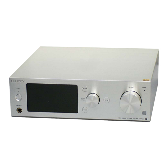
Sony HAP-S1 Service Manual
Hdd audio player system
Hide thumbs
Also See for HAP-S1:
- User manual (127 pages) ,
- Reference manual (50 pages) ,
- Quick start manual (19 pages)
Table of Contents
Quick Links
SERVICE MANUAL
Ver. 1.0 2013.10
Note:
Be sure to keep your PC used for service and
checking of this unit always updated with the
latest version of your anti-virus software.
In case a virus affected unit was found during
service, contact your Service Headquarters.
AUDIO POWER SPECIFICATIONS
POWER OUTPUT AND TOTAL HARMONIC DISTORTION (for the USA and Canada
only):
With 4 ohm loads, both channels driven, from 20 - 20,000Hz; rated 32 watts per channel
minimum RMS power, with no more than 10 % total harmonic distortion from 250 milliwatts to
rated output.
Amplifier section
POWER OUTPUT: 40 W + 40 W (4 ohms, 1 kHz, THD 10%)
Rated Power Output: 35 W + 35 W (4 ohms, 1 kHz, THD 0.9%)
Speaker impedance match: 4 ohms - 16 ohms
S/N ratio: 100 dB (20 kHz LPF, A Network)
Frequency response: 10 Hz - 100 kHz (+0 dB, –3 dB) (4 ohms, LINE IN)
Network section
Wired LAN
1000BASE-T/100BASE-TX/10BASE-T
Wireless LAN
Compatible standards: IEEE 802.11 b/g/n
Frequency band/channel: 2.4 GHz band, channels 1-11 (models for the USA and Canada),
channels 1-13 (models for Europe)
HDD section
Capacity
500 GB (*)
*
Some portions of the capacity are used for data management. Therefore, the capacity a user can
use is less than 500 GB.
Supported playback format
DSD (DSF, DSDIFF), LPCM (WAV, AIFF), FLAC, ALAC, ATRAC Advanced Lossless, ATRAC, MP3,
AAC, WMA (2 channels)
Jack section
Input section
COAXIAL IN
Input impedance: 75 ohms
Supported playback format: LPCM 2ch
Sampling frequency: 44.1 kHz, 48 kHz, 88.2 kHz, 96 kHz, 176.4 kHz, 192 kHz
Quantization bits: 16 bits, 24 bits
OPTICAL IN
Supported playback format: LPCM 2ch
Sampling frequency: 44.1 kHz, 48 kHz, 88.2 kHz, 96 kHz
Quantization bits: 16 bits, 24 bits
9-893-833-01
Sony Corporation
2013J33-1
©
2013.10
Published by Sony Techno Create Corporation
SPECIFICATIONS
LINE IN 1, 2
Input sensitivity: 500 mV
Input impedance: 100 kilohms
Output section
Output jacks
LINE OUT
Output impedance: 2.2 kilohms
2 Hz - 80 kHz (–3 dB)
PHONES (headphone jack)
Stereo jack: 8 ohms or higher
EXT port
Type A USB, Hi-Speed USB, for connecting an external hard disk drive
General and others
Power requirements
Models for the USA and Canada: AC 120 V 60 Hz
Models for Europe: AC 230 V 50/60 Hz
Power consumption
Models for the USA and Canada
On: 80 W
During standby mode (when [Network Standby] is set to [Off]): 0.3 W
During standby mode (when [Network Standby] is set to [On] and a wired LAN is used): 2.6 W
During standby mode (when [Network Standby] is set to [On] and a wireless LAN is used): 2.8
W
Models for Europe
On: 85 W
During standby mode (when [Network Standby] is set to [Off]): 0.3 W
During standby mode (when [Network Standby] is set to [On] and a wired LAN is used): 2.6 W
During standby mode (when [Network Standby] is set to [On] and a wireless LAN is used): 2.8
W
Dimensions (approx.) (w/h/d)
265 mm × 88 mm × 304 mm (10 1/2 in. × 3 1/2 in. × 12 in.) including projecting parts and
controls
Mass (approx.)
5.8 kg (12 lbs 12 5/8 oz)
Supplied accessories
Remote control (1)
R03 (size-AAA) batteries (2)
AC power cord (mains lead) (1)
LAN cable (1)
Design and specifications are subject to change without notice.
HDD AUDIO PLAYER SYSTEM
HAP-S1
US Model
Canadian Model
AEP Model
UK Model
Table of Contents

Related Manuals for Sony HAP-S1


Summary of Contents for Sony HAP-S1
-
Page 1: Specifications
AC power cord (mains lead) (1) Quantization bits: 16 bits, 24 bits LAN cable (1) Design and specifications are subject to change without notice. HDD AUDIO PLAYER SYSTEM 9-893-833-01 Sony Corporation 2013J33-1 © 2013.10 Published by Sony Techno Create Corporation... - Page 2 12 TONE ANALYSIS and its logo are trademarks of Sony Corporation. aged by heat. “DSEE” is a registered trademark of Sony Corporation. SensMe™ and the SensMe™ logo are trademarks or registered trademarks of Sony Ericsson Mobile Communications AB. FLEXIBLE CIRCUIT BOARD REPAIRING Microsoft, Windows, Windows Vista and Windows Media are either trademarks or registered trademarks of Microsoft Corporation in the United States and/or other countries.
-
Page 3: Table Of Contents
HAP-S1 TABLE OF CONTENTS SERVICING NOTES 5-5. Block Diagram - POWER SUPPLY Section - ....44 ..........5-6. Printed Wiring Boards - MAIN Section - ....... 46 5-7. Schematic Diagram - MAIN Section (1/9) - ....47 DISASSEMBLY 5-8. Schematic Diagram - MAIN Section (2/9) - ....48 2-1. -
Page 4: Servicing Notes
HAP-S1 SECTION 1 SERVICING NOTES UNLEADED SOLDER NOTE OF REPLACING THE D218, IC350 AND IC351 Boards requiring use of unleaded solder are printed with the lead- ON THE AMP BOARD AND THE COMPLETE AMP free mark (LF) indicating the solder contains no lead. - Page 5 HAP-S1 NOTE OF REPLACING THE COMPLETE MAIN BOARD When the complete MAIN board is replaced, the following set- The MAC address for the wireless LAN has been changed tings that is recorded on the MAIN board are cleared, and returned by this repair.
- Page 6 HAP-S1 MAIN BOARD SERVICE POSITION front panel block stand insulation MAIN board U-COM board DCDC BOARD SERVICE POSITION DCDC board insulation front panel block...
-
Page 7: Disassembly
HAP-S1 SECTION 2 DISASSEMBLY • This set can be disassembled in the order shown below. 2-1. DISASSEMBLY FLOW 2-2. SIDE PANEL (L/R) ASSY (Page 9) 2-3. FRONT PANEL (ALG) BLOCK, FUSE (F902) (Page 10) 2-4. HP BOARD 2-8. WLAN/BT COMBO CARD (WBC1) - Page 8 HAP-S1 From previous page. 2-18. SUB FRAME BLOCK (Page 20) 2-19. SUB FRAME BLOCK WIRES 2-23. POWER TRANSFORMER (T1) (Page 21) (Page 23) 2-20. U-COM BOARD 2-21. FPGA DSP BOARD 2-24. ANT HOLDER BLOCK 2-26. BRACKET (DCDC-F) (Page 22) (Page 22)
-
Page 9: Side Panel (L/R) Assy
HAP-S1 Note: Follow the disassembly procedure in the numerical order given. 2-2. SIDE PANEL (L/R) ASSY 2 Insert a tweezers etc. to hole of chassis and slide the hook in the direction of the arrow. 1 flat screw 5 claw... -
Page 10: Front Panel (Alg) Block, Fuse (F902)
HAP-S1 2-3. FRONT PANEL (ALG) BLOCK, FUSE (F902) 2 four screws (BTP3 Note 1: Please spread a sheet under a unit not to panel. – Rear bottom view – 1 two screws (BV3) 3 claw 4 Remove the front panel (ALG) block in the direction of an arrow. -
Page 11: Hp Board
HAP-S1 2-4. HP BOARD 2 Remove the HP board block in the direction of an arrow. 5 HP board 1 screw (BVTP2.6) 3 screw (BV3) 4 bracket (HP) 1 screw (BVTP2.6) – Front panel (ALG) block rear bottom view –... -
Page 12: Lcd Holder Block
HAP-S1 2-6. LCD HOLDER BLOCK 2 LCD holder block 1 screw (BVTP2.6) – Front panel (ALG) block rear bottom view – 2-7. LCD PANEL (LCD1) 4 LCD cushion (B) 3 LCD cushion (A) 1 LCD flexible board (CN002) o itio o Note: Attach to fit the corner. -
Page 13: Wlan/Bt Combo Card (Wbc1)
HAP-S1 2-8. WLAN/BT COMBO CARD (WBC1) DCDC board 3 flat screw saranet cushion 2 screw (BV3) saranet cushion saranet cushion 1 two saranet cushions 1 saranet cushion 4 Remove the WLAN/BT COMBO card block in the direction of an arrow. -
Page 14: Clamp Filter (Ferrite Core) (Fc1, Fc2)
HAP-S1 2-9. CLAMP FILTER (FERRITE CORE) (FC1, FC2) DCDC board cable tie 1 Cut the cable tie. Note: In reassembling, use new cable tie to fasten the clamp same as before. 3 connector (CN2405) 5 clamp filter (ferrite core) (FC2) -
Page 15: Hdd (Hdd1)
HAP-S1 2-11. HDD (HDD1) Note 1: When the hard disk drive (Ref. No. HDD1) is replaced, refer to “NOTE OF REPLACING THE HARD DISK DRIVE (Ref. No. HDD1)” on page 4. DCDC board 7 HDD (HDD1) 6 bracket (HDD) 3 HDD connector... -
Page 16: Allegro-Ant-R Board
HAP-S1 2-13. ALLEGRO-ANT-R BOARD coaxial cable (U.FL connector) (WR2) sheet (WA-M) 5 mm tape (WA-M) coaxial cable connector facing up (U.FL connector) (WR2) ANT holder wrapped side no wrapped side 1 tape (WA-L) 3 four claws ALLEGRO-ANT-R board 5 coaxial cable (U.FL connector) (WR2) -
Page 17: Clamp Filter (Ferrite Core) (Fc4)
HAP-S1 2-14. CLAMP FILTER (FERRITE CORE) (FC4) lead pin lead pin DIGITAL IO board lead pin clamp filter (ferrite core) (FC4) 2 connector 3 clamp filter (ferrite core) (CN4003) (FC4) 1 Remove wires from three lead pins. DIGITAL IO board... -
Page 18: Dcdc Board-1
HAP-S1 2-15. DCDC BOARD-1 DIGITAL IO board lead pin lead pin 3 connector 5 connector (CN4013) (CN4009) 2 connector (CN4005) 1 Remove wires from three lead pins. lead pin 4 connector (CN4008) DIGITAL IO board DCDC board wire holder... -
Page 19: Dcdc Board-2
HAP-S1 2-16. DCDC BOARD-2 5 Remove the DCDC board block 4 three screws in the direction of an arrow. (BV3) 3 connector (CN2408) 2 clamp filter (ferrite core) (FC5) 1 Cut the cable tie. Note: In reassembling, use new cable tie to fasten the clamp same as before. -
Page 20: Wire Holder
HAP-S1 2-17. WIRE HOLDER 2 claw 5 wire holder 2 claw 4 claw 4 claw 3 Remove the wire holder in the direction of an arrow. 1 connector (CN213) 2-18. SUB FRAME BLOCK 4 claw 3 flat screw 7 Draw out the wire. -
Page 21: Sub Frame Block Wires
HAP-S1 2-19. SUB FRAME BLOCK WIRES saranet cushion saranet cushion saranet cushion clamp MAIN board FPGA DSP board – – 3 Remove wires from the clamp. 2 flexible flat cable (24P) (CN4006) qd harness (S-001) (WR5) 6 connector (CN1001) (CN701) -
Page 22: U-Com Board
HAP-S1 2-20. U-COM BOARD 2 U-COM board 1 three screws (BV3) 2-21. FPGA DSP BOARD 2 connector (CN402) 3 FPGA DSP board 1 two screws (BV3) 1 two screws (BV3) -
Page 23: Main Board
HAP-S1 2-22. MAIN BOARD Note: When the complete MAIN board is replaced, refer to “NOTE OF REPLACING THE COMPLETE MAIN BOARD” and “CHECK- ING METHOD OF NETWORK CONNECTION” on page 5. 4 Draw out two wires. 7 connector 9 MAIN board... -
Page 24: Ant Holder Block (Left Side)
HAP-S1 2-24. ANT HOLDER BLOCK (LEFT SIDE) 4 ANT holder block (left side) 2 Remove the ANT holder block (left side) in the direction of an arrow. 3 three claws 1 flat screw... -
Page 25: Allegro-Ant-L Board
HAP-S1 2-25. ALLEGRO-ANT-L BOARD coaxial cable (U.FL connector) (WR1) sheet (WA-M) coaxial cable (U.FL connector) (WR1) 5 mm ANT holder tape (WA-M) wrapped side connector facing up no wrapped side Note: The ALLEGRO-ANT-L board is not covered in the servicing. -
Page 26: Bracket (Dcdc-F)
HAP-S1 2-26. BRACKET (DCDC-F) 1 screw (BV3) 4 Cut the cable tie. Note: In reassembling, use new bracket (DCDC-F) cable tie to fasten the clamp 6 bracket (DCDC-F) same as before. cable tie 1 screw (BV3) 2 Remove the bracket (DCDC-F) block in the direction of an arrow. -
Page 27: Amp Board-1
HAP-S1 2-28. AMP BOARD-1 SPTM board lead pin lead pin STANBY board 2 bracket (DIGITAL) lead pin lead pin 5 connector (CN1901) 6 connector (CN701) lead pin 3 Remove wires from 1 screw (BV3) two lead pins. sleeve ferrite clamp... -
Page 28: Amp Board-2
HAP-S1 2-29. AMP BOARD-2 Note: When the complete AMP board is replaced, refer to “NOTE OF REPLACING THE D218, IC350 AND IC351 ON THE AMP BOARD AND THE COMPLETE AMP BOARD” on page 4. 2 clamp 1 screw (BV3) 3 bracket (DCDC-R) -
Page 29: Sptm Board
HAP-S1 2-31. SPTM BOARD (AEP, UK) 3 four canoe clips 4 SPTM board 2 Remove the SPTM board block in the direction of an arrow. 1 two screws (BV3) 2-32. AC INLET 2P (AC1) 3 clamp filter (ferrite core) 2 Cut the cable tie. -
Page 30: Stanby Board
HAP-S1 2-33. STANBY BOARD (AEP, UK) 3 label fuse (T.L) 1 screw (BV3) 1 screw (BV3) 1 two screws (BV3) 4 STANBY board 2 Remove the STANBY board block in the direction of an arrow. 2-34. DAC BOARD flexible flat cable (22P) -
Page 31: Test Mode
HAP-S1 SECTION 3 TEST MODE 1. Entering Method of The Service Diag Mode 4. Operation of The Service DIAG Mode 4-1. Version Info Procedure: It can display the version information. 1. Connect the power cord to an outlet. 2. After becoming the standby state, while holding down two... - Page 32 HAP-S1 4-3. LED/KEY 4-3-3. KEY Check It can check the keys and knobs. Procedure: 1. Enter the service DIAG mode. Procedure: (Refer to “1. Entering Method of The Service DIAG Mode” on 1. Enter the “3. LED/KEY” mode. page 31) (Refer to “4-3.
- Page 33 HAP-S1 4-4. LCD/Others 4-4-2. LCD Back light Check It can check the liquid crystal display back light. Procedure: 1. Enter the service DIAG mode. Procedure: (Refer to “1. Entering Method of The Service DIAG Mode” on 1. Enter the “4. LCD/Others” mode.
- Page 34 5. The fan motor is changed to slow speed. 6. SMART Long Test (2-4 hours) 6. Rotate the [PUSH ENTER] knob to select the “3. fan mid (HAP-S1 only)” and press the [PUSH ENTER] knob. 5.HDD 7. The fan motor is changed to medium speed.
- Page 35 HAP-S1 6. The SMART data is saved as a text fi le in the USB memory. 4-6. Audio (The fi le name is “hap_smart_data_xxxxx_yyyyy.log (xxxxx: hard disk drive model name, yyyyy: hard disk drive serial Procedure: number)) 1. Enter the service DIAG mode.
- Page 36 HAP-S1 4-6-2. Select Input 4-7-1. Network/Module Info It can select the external audio input terminal. It can display the wireless network and module information. Procedure: Procedure: 1. Enter the “6. Audio” mode. 1. Enter the “7. WiFi” mode. (Refer to “4-6. Audio” on page 35) (Refer to “4-7.
- Page 37 HAP-S1 4-8. Ether 4-8-2. Ping It can display the results indicating whether or not the gateway Procedure: responded to the PING. Note: This mode supports only DHCP. 1. Connect the main unit to the router with the network LAN cable.
-
Page 38: Electrical Check
HAP-S1 SECTION 4 ELECTRICAL CHECK HDD CHECK 7. When the result of test is OK, following screen is displayed on the liquid crystal display. It can check the result of hard disk drive test. 5-6.SMART Long Test 1. Operation of The SMART Long Test SMART Test is Succeded. - Page 39 HAP-S1 3. Checking Method of The SMART Test Result Procedure: 1. After the SMART test is completed, press the [PUSH ENTER] knob or [BACK] key to return to the “5. HDD” menu. 2. Rotate the [PUSH ENTER] knob to select the “4. SMART Data Read(Need USB Memory)”...
-
Page 40: Diagrams
HAP-S1 SECTION 5 DIAGRAMS 5-1. BLOCK DIAGRAM - HDD/USB/LAN/FPGA/DSP Section - HDD1 FPGA AUDIO DSP HARD DISK DRIVE IC101 (1/3) IC001 (1/2) IC702 HR+0 B14 SATA_RXP PICE_TXP J2 GXB_RX0p IO/VREFB7N0 22 DAI_D1 IO/DIFFCLK_T11N/DQ0T 24 DAI_SCLK HR–0 A14 SATA_RXM PICE_TXM J1 GXB_RX0n... -
Page 41: Block Diagram - Digital Audio Input Section
HAP-S1 5-2. BLOCK DIAGRAM - DIGITAL AUDIO INPUT Section - DATA/CLOCK SELECTOR D/A CONVERTER IC4007 IC405 DIGITAL AUDIO INTERFACE RECEIVER IC4004 DATA_DSDL IOUTL+ 25 LINE AMP L, R OPTICAL >002B DATA IC402 OPTICAL IN RECEIVER RXIN1 DATAOUT 16 IOUTL– 26... -
Page 42: Block Diagram - Analog Audio Input/Output Section
HAP-S1 5-3. BLOCK DIAGRAM - ANALOG AUDIO INPUT/OUTPUT Section - J401 (2/2) L, R >002B BUFFER D/A DIRECT (Page 41) IC415 LINR OUT SIGNAL PATH MUTING MUTING : AUDIO (ANALOG) Q400 Q401 : AUDIO IN (ANALOG) MUTING CONTROL SWITCH Q217 – 219... -
Page 43: Block Diagram - Memory/Panel Section
HAP-S1 5-4. BLOCK DIAGRAM - MEMORY/PANEL Section - LCD1 LIQUID CRYSTAL SD-RAM SYSTEM CONTROLLER IC301 IC101 (2/3) DISPLAY IC5006 (4/5) REMOTE CONTROL DQL0 – DQL7 DRAM_D0 – DRAM_D7 65 SIRCS IN DISP_DAT0 – RECEIVER B0 – B7 DISP_DAT7 IC1002 DQU0 – DQU7 DRAM_D8 –... -
Page 44: Block Diagram - Power Supply Section
HAP-S1 5-5. BLOCK DIAGRAM - POWER SUPPLY Section - USB_OTG_VBUS EIM_D22 EIM_D21 D1003, 1004 USB_H1_VBUS VBUS WLAN/BT COMBO CARD SWITCH VBUS Q1001, 1002 ENET_TXD1 DC/DC VCC 1.2V CONVERTER IC101 +2.5V VCC_2.5V REGULATOR IC102 VDD_3.3V, B+ SWITCH CIRRUS_3.3V IC103 +3.3V CSI0_VSYNC +3.3V... - Page 45 HAP-S1 THIS NOTE IS COMMON FOR PRINTED WIRING BOARDS AND SCHEMATIC DIAGRAMS. • Circuit Boards Location (In addition to this, the necessary note is printed in each block.) For Printed Wiring Boards. For Schematic Diagrams. WLAN/BT COMBO card Note: Note:...
-
Page 46: Printed Wiring Boards - Main Section
HAP-S1 5-6. PRINTED WIRING BOARDS - MAIN Section - • See page 45 for Circuit Boards Location. • : Uses unleaded solder. WBC1 WLAN/BT COMBO CARD U-COM DIGITAL IO (Page 66) (Page 56) >02P >07P MAIN BOARD BOARD BOARD ALLEGRO-ANT-L BOARD... -
Page 47: Schematic Diagram - Main Section (1/9)
HAP-S1 5-7. SCHEMATIC DIAGRAM - MAIN Section (1/9) - • See page 86 for IC Pin Function Description. MAIN BOARD (1/9) (2/10) (3/10) (1/10) IC101 IC101 IC101 (Chip Size Package) (Chip Size Package) IC101 IC101 C190 MCIMX6D5EYM10AC MCIMX6D5EYM10AC (Chip Size Package) -
Page 48: Schematic Diagram - Main Section (2/9)
HAP-S1 5-8. SCHEMATIC DIAGRAM - MAIN Section (2/9) - • See page 73 for Waveforms. • See page 78 for IC Block Diagrams. MAIN BOARD (2/9) IC204 +3.3V REGULATOR IC204 MM3464A33NRE FL201 R261 VOUT >105S 3.3V GND1 GND2 MAIN USB_5V... -
Page 49: 5-9. Schematic Diagram - Main Section (3/9)
HAP-S1 5-9. SCHEMATIC DIAGRAM - MAIN Section (3/9) - • See page 86 for IC Pin Function Description. MAIN BOARD (3/9) IC101 (4/10) (Chip Size Package) IC101 MCIMX6D5EYM10AC CL301 D0DQ0 AC14 D0A0 DRAM_D0 DRAM_A0 D0DQ1 CL302 AB14 D0A1 DRAM_D1 DRAM_A1... -
Page 50: Schematic Diagram - Main Section (4/9)
HAP-S1 5-10. SCHEMATIC DIAGRAM - MAIN Section (4/9) - See page 78 for IC Block Diagrams. • See page 86 for IC Pin Function Description. (Page 60) MAIN BOARD (4/9) FPGA DSP FL401 >03S BOARD (2/3) CN401 CN402 FL400 GND2... -
Page 51: Schematic Diagram - Main Section (5/9)
HAP-S1 5-11. SCHEMATIC DIAGRAM - MAIN Section (5/9) - • See page 86 for IC Pin Function Description. MAIN BOARD (5/9) CL511 R509 R501 R502 FL501 C513 >110S 3.3V C514 MAIN BOARD (2/9) (Page 48) CL518 (6/10) IC101 NC_M7 NC_H1... -
Page 52: Schematic Diagram - Main Section (6/9)
HAP-S1 5-12. SCHEMATIC DIAGRAM - MAIN Section (6/9) - • See page 73 for Waveforms. • See page 86 for IC Pin Function Description. MAIN BOARD (6/9) IC101 (7/10) C622 R648 R649 R626 (Chip Size Package) IC101 R605 R601 MCIMX6D5EYM10AC... -
Page 53: Schematic Diagram - Main Section (7/9)
HAP-S1 5-13. SCHEMATIC DIAGRAM - MAIN Section (7/9) - • See page 73 for Waveforms. • See page 86 for IC Pin Function Description. MAIN BOARD (7/9) >119S DISP0_PWR_EN IC701 Q704 MAIN SSM3J134TU,LSOYF BOARD DC/DC CONVERTER (6/9) IC701 TB62752AFUG(O,EL) (Page 52) -
Page 54: Schematic Diagram - Main Section (8/9)
HAP-S1 5-14. SCHEMATIC DIAGRAM - MAIN Section (8/9) - • See page 86 for IC Pin Function Description. MAIN BOARD (8/9) >120S DISP0_RST R854 DIAG_EN MAIN BOARD IC101 (9/10) (7/9) (Page 53) (Chip Size Package) IC101 MCIMX6D5EYM10AC EIM_LBA CL805 EIM_BCLK... -
Page 55: Schematic Diagram - Main Section (9/9)
HAP-S1 5-15. SCHEMATIC DIAGRAM - MAIN Section (9/9) - • See page 78 for IC Block Diagrams. • See page 86 for IC Pin Function Description. MAIN BOARD (9/9) IC101 (10/10) CN1001 (Chip Size Package) IC101 C1013 MCIMX6D5EYM10AC 0.01 L1001 >103S... -
Page 56: Printed Wiring Board - Digital Io Board
HAP-S1 5-16. PRINTED WIRING BOARD - DIGITAL IO Board - • See page 45 for Circuit Boards Location. • : Uses unleaded solder. (Page 46) (Page 46) DIGITAL IO BOARD (COMPONENT SIDE) MAIN MAIN >07P >04P BOARD BOARD (NC) CN1003... -
Page 57: Schematic Diagram - Digital Io Board
HAP-S1 5-17. SCHEMATIC DIAGRAM - DIGITAL IO Board - • See page 73 for Waveforms. • See page 78 for IC Block Diagrams. DIGITAL IO BOARD CN4008 CN4003 CL4026 CL4109 D_REG_EN CL4027 D_SEL CL4110 D_SEL CL4029 TRDP_0 D_ST_DATA CL4111 D_ST_DATA... -
Page 58: Printed Wiring Board - Fpga Dsp Board
HAP-S1 5-18. PRINTED WIRING BOARD - FPGA DSP Board - • See page 45 for Circuit Boards Location. • : Uses unleaded solder. (Page 56) DIGITAL IO >11P BOARD FPGA DSP BOARD (SIDE A) CN4006 FFC2 CL302 CL301 CL504 CL503... -
Page 59: Schematic Diagram - Fpga Dsp Board (1/3)
HAP-S1 5-19. SCHEMATIC DIAGRAM - FPGA DSP Board (1/3) - • See page 78 for IC Block Diagrams. • See page 86 for IC Pin Function Description. FPGA DSP BOARD (1/3) IC001 (1/4) FPGA (Chip Size Package) CL201 IC001 CL207... -
Page 60: Schematic Diagram - Fpga Dsp Board (2/3)
HAP-S1 5-20. SCHEMATIC DIAGRAM - FPGA DSP Board (2/3) - • See page 86 for IC Pin Function Description. (Page 50) MAIN >03S BOARD (4/9) FPGA DSP BOARD (2/3) CN402 CN401 CL423 MAIN_5V >131S PCIE_REFCLK_N PCIE_REFCLK_P FPGA DSP BOARD CL424... -
Page 61: Schematic Diagram - Fpga Dsp Board (3/3)
HAP-S1 5-21. SCHEMATIC DIAGRAM - FPGA DSP Board (3/3) - • See page 73 for Waveforms. • See page 86 for IC Pin Function Description. FPGA DSP BOARD (3/3) CN506 IC001 (4/4) DIRGND CL505 DATAR_DSDRD FPGA DIRGND CL506 (Chip Size Package) -
Page 62: Printed Wiring Board - Dac Board
HAP-S1 5-22. PRINTED WIRING BOARD - DAC Board - • See page 45 for Circuit Boards Location. • : Uses unleaded solder. DAC BOARD (COMPONENT SIDE) CL432 R461 R472 C463 EE400 IC415 C462 EE402 (CHASSIS) (CHASSIS) C459 R478 C413 C449... -
Page 63: Schematic Diagram - Dac Board
HAP-S1 5-23. SCHEMATIC DIAGRAM - DAC Board - • See page 73 for Waveforms. • See page 78 for IC Block Diagrams. (Page 57) DIGITAL IO >12S BOARD CN4007 DAC BOARD FFC3 J401 C437 C438 C444 C443 C408 CL421 R440... -
Page 64: Printed Wiring Board - Amp Board
HAP-S1 5-24. PRINTED WIRING BOARD - AMP Board - • See page 45 for Circuit Boards Location. • : Uses unleaded solder. AMP BOARD SPTM (CONDUCTOR SIDE) (Page 68) >16P BOARD AMP BOARD (COMPONENT SIDE) CN701 TH200 C214 JL202 R350... -
Page 65: Schematic Diagram - Amp Board
HAP-S1 5-25. SCHEMATIC DIAGRAM - AMP Board - • See page 78 for IC Block Diagrams. AMP BOARD CN207 CL257 >16S CL256 SPTM CL255 BOARD CL254 -28.4 -28.4 CN701 Q205 Q202 (Page 69) 2SA2154MFV(TL3S 2SA2154MFV(TL3S R222 C244 DC DETECT C245... -
Page 66: Printed Wiring Board - U-Com Board
HAP-S1 5-26. PRINTED WIRING BOARD - U-COM Board - • See page 45 for Circuit Boards Location. • : Uses unleaded solder. (Former type) (Page 70) (Page 71) (New type) KEY JOG BOARD KEY JOG BOARD >21P >24P CN5009 CN5009... -
Page 67: Schematic Diagram - U-Com Board
HAP-S1 5-27. SCHEMATIC DIAGRAM - U-COM Board - • See page 73 for Waveforms. • See page 78 for IC Block Diagrams. • See page 86 for IC Pin Function Description. U-COM BOARD D5011 RB551V-30TE-17 C5033 C5034 C5035 C5036 R5049 R5050 2.2k... -
Page 68: Printed Wiring Boards - Output/Lcd Section
HAP-S1 5-28. PRINTED WIRING BOARDS - OUTPUT/LCD Section - • See page 45 for Circuit Boards Location. • : Uses unleaded solder. (Page 46) MAIN >06P BOARD ALLEGRO-LCD BOARD (SIDE A) CN703 FFC1 CN001 SPTM BOARD (COMPONENT SIDE) HP BOARD... -
Page 69: Schematic Diagram - Output/Lcd Section
HAP-S1 5-29. SCHEMATIC DIAGRAM - OUTPUT/LCD Section - SPTM BOARD ALLEGRO-LCD BOARD CN001 CN002 VELD– VELD– C703 C702 R703 R701 0.01 220p TB701 VLED+ VLED+ CN701 CL700 R[0] R[0] >16S CL701 L701 – R[1] R[1] R[2] R[2] CL702 SPEAKERS BOARD... -
Page 70: Printed Wiring Boards - Key Section (1/2)
HAP-S1 5-30. PRINTED WIRING BOARDS - KEY Section (1/2) - • See page 45 for Circuit Boards Location. • : Uses unleaded solder. (Former type) PENC BOARD PENC BOARD (COMPONENT SIDE) (CONDUCTOR SIDE) KEY JOG BOARD (COMPONENT SIDE) CN5310 R5117... -
Page 71: Printed Wiring Boards - Key Section (2/2)
HAP-S1 5-31. PRINTED WIRING BOARDS - KEY Section (2/2) - • See page 45 for Circuit Boards Location. • : Uses unleaded solder. (New type) (Page 70) PENC BOARD >25P KEY JOG BOARD (COMPONENT SIDE) CN5301 KEY JOG AND POWER KEY BOARDS DISCRIMINATION In this unit, the KEY JOG and POWER KEY boards have been changed in the midway of production. -
Page 72: Schematic Diagram - Key Section
HAP-S1 5-32. SCHEMATIC DIAGRAM - KEY Section - KEY JOG BOARD R5117 CN5009 CL5231 EN5004 R5118 ROTARY CL5232 ENCODER STB5 VOLUME CL5233 C5050 C5052 STB3.3 0.001 0.001 CL5234 VLJG+ PENC BOARD CL5235 EN5005 VLJG– CL5236 ROTARY FFC4 SLJG+ ENCODER CL5237 PUSH SLJG–... - Page 73 HAP-S1 • Waveforms – MAIN Board – – DIGITAL IO Board – – FPGA DSP Board – – DAC Board – – U-COM Board – IC202 1 (BST) IC4004 qd (MCKOUT) IC4007 7 (Y1) IC701 5, 6 IC407 5 (Y) IC5006 rk (XTALO) 3.7 Vp-p...
-
Page 74: Printed Wiring Board - Dcdc Board
HAP-S1 5-33. PRINTED WIRING BOARD - DCDC Board - • See page 45 for Circuit Boards Location. • : Uses unleaded solder. HDD1 (Page 56) HARD DISK DRIVE DIGITAL IO (2/2) >13P BOARD DCDC BOARD DCDC BOARD (CONDUCTOR SIDE) (COMPONENT SIDE) -
Page 75: Schematic Diagram - Dcdc Board
HAP-S1 5-34. SCHEMATIC DIAGRAM - DCDC Board - • See page 73 for Waveforms. • See page 78 for IC Block Diagrams. DCDC BOARD CL2416 L2401 R2411 D2406 4.7uH IC2402 DZ2J062M0L DC/DC CONVERTER IC2402 CN2403 RT7256ALZSP C2412 R2412 STBY FET ON/OFF R2407 10.2... -
Page 76: Printed Wiring Board - Stanby Board
HAP-S1 5-35. PRINTED WIRING BOARD - STANBY Board - • See page 45 for Circuit Boards Location. • : Uses unleaded solder. STANBY BOARD STANBY BOARD (COMPONENT SIDE) (CONDUCTOR SIDE) CN1904 ~AC IN LND901 D1901 D1902 PATTERN SPARK-GAP D1906 C1903... -
Page 77: Schematic Diagram - Stanby Board
HAP-S1 5-36. SCHEMATIC DIAGRAM - STANBY Board - STANBY BOARD MAIN POWER TRANSFORMER Q1905 SSM6J50TU(T5RSONYF >23S CN1903 DCDC BOARD Q1903 - 1905 CN2408 B+ SWITCH (Page 75) R1908 R1909 CL1905 470k 220k >17S R1913 470k R1910 BOARD Q1904 Q1903 CN201... - Page 78 HAP-S1 • IC Block Diagrams – MAIN Board – IC201 BU33TD3WG-TR IC203 TPS54295PWPR VREG5 VREG5 CONTROL CONTROL VIN1 1 VIN2 LOGIC LOGIC VOLTAGE VBST1 VBST2 – REFERENCE VOUT XCON XCON OVER CURRENT PROTECTION THERMAL CH1 MIN-OFF CH2 MIN-OFF SHUTDOWN TIMER...
- Page 79 HAP-S1 IC205, 401 PST8429UL IC701 TB62752AFUG (O, EL) 6 FB GND 1 SHUTDOWN SHDN 1 FUNCTION 5 GND ERROR CURRENT VREF LIMIT OVER VOLTAGE OVD 2 DETECTION VIN 3 REFERENCE – (1.1MHz) CONTROL VDD 2 4 SW IC1001 TPS2553DBVR RREVERSE VOLTAGE –...
- Page 80 HAP-S1 IC4004 LC89075WA-H 62 61 60 59 58 57 56 RXIN5 RXIN6 RXIN7 RXIN8 MUX 15:3 GROUP: C S/PDIF GROUP: D LPF 1 DIGITAL INTERFACE RECEIVER PGND 2 MASTER CLOCK MCKIN 3 BIT CLOCK BCKIN 4 LR CLOCK or DSD...
-
Page 81: Fpga Dsp Board
HAP-S1 IC4008 CS230002-CZZR VD 1 GND 2 OUT_EN CLK_OUT 3 FRACTIONAL-N FILTN FREQUENCY FILTP SYNTHESIZER LOCK 4 M [1:0] OUTPUT TO INPUT 00 = 1 CLOCK RADIO 128 Hz BW DIGITAL PLL 01 = 2 & FRACTIONAL N LOGIC 10 = 4... - Page 82 HAP-S1 IC103 BD2231G-TR VIN 1 VOUT UNDER-VOLTAGE LOCKOUT GND 2 CHARGE THERMAL EN 3 PUMP SHUTDOWN OVER-CURRENT DELAY PROTECTION COUNTER – DAC Board – IC403 MM1836A50NRE IC404, 413, 414 NJM2871BF33-TE2 CONT 1 BIAS CURRENT LIMIT – THERMAL REGULATOR PROTECTION VOUT...
- Page 83 HAP-S1 IC407, 410 TC7WH157FK 11 7 11 6 SELECT EN G GND 4 IC411 HD74LV161ATELL CLR 1 16 VCC 15 RCO CLK 2 1, 2T/1C3 14 QA 1, 2T/1C3 13 QB 1, 2T/1C3 12 QC 1, 2T/1C3 11 QD ENP 7...
- Page 84 HAP-S1 – AMP Board – IC206 NJW1194 INA1 1 INB1 INA2 2 INB2 INA3 3 INB3 INA4 4 INB4 GND 5 DCCAP_A 6 DCCAP_B GND 7 OUTA 8 OUTB VDDOUT 9 DATA 10 ADR1 CONTROL CLOCK 11 ADR0 LOGIC LATCH 12 V–...
- Page 85 HAP-S1 – U-COM Board – IC5004 BU4229F-TR GND 1 VREF – VOUT VDD 2 IC5005 TC74VHC4052AFT (EK) 0Y 1 2Y 2 Y-COM 3 X-COM 3Y 4 1Y 5 INH 6 GND 7 GND 8 – DCDC Board – IC2402 – 2404 RT7256ALZSP...
- Page 86 HAP-S1 • IC Pin Function Description MAIN BOARD IC101 MCIMX6D5EYM10AC (MPU) Pin No. Pin Name Description PCIE_REXT Terminal for the Impedance calibration PCIE_TXM Transmit data (negative) output to the FPGA GND3 Ground terminal FA_ANA Not used USB_OTG_DP Two-way USB data (positive) with the USB connector...
- Page 87 HAP-S1 Pin No. Pin Name Description RTC_XTALO Real time clock output terminal (32.768 kHz) GND24 Ground terminal POR_B Reset signal input from reset signal generator and system controller “L”: reset BOOT_MODE0 Boot mode setting terminal Fixed at “L” SD3_DAT5 Not used...
- Page 88 HAP-S1 Pin No. Pin Name Description RGMII_TD2 RGMII transmit data output to the ethernet transceiver EIM_EB2 Boot mode setting terminal Fixed at “L” EIM_D22 VBUS power on/off control signal output terminal for the USB connector “H”: power on E24, E25...
- Page 89 HAP-S1 Pin No. Pin Name Description GND40 Ground terminal VDDARM_CAP1 Internal regulator output terminal VDDARM_IN1 Power supply terminal for the cores regulator (+1.42V) GND41 Ground terminal VDDSOC_IN1 Power supply terminal for the SOC and PU regulators (+1.42V) VDDPU_CAP1 Internal regulator output terminal...
- Page 90 HAP-S1 Pin No. Pin Name Description EIM_DA3 Boot mode setting terminal Fixed at “L” EIM_DA6 Boot mode setting terminal Fixed at “H” CSI0_DAT13 Serial data or program data input from the system controller GND58 Ground terminal CSI0_DAT17, L3, L4 Not used...
- Page 91 HAP-S1 Pin No. Pin Name Description VDDARM23_CAP6 Internal regulator output terminal Not used VDD_CACHE_CAP Internal regulator output terminal (+1.1V) VDDARM_CAP6 Internal regulator output terminal VDDARM_IN6 Power supply terminal for the cores regulator (+1.42V) GND67 Ground terminal VDDSOC_IN6 Power supply terminal for the SOC and PU regulators (+1.42V)
- Page 92 HAP-S1 Pin No. Pin Name Description GPIO_2, GPIO_9, T1 to T5 GPIO_6, GPIO_1, Not used GPIO_0 KEY_COL4 Not used KEY_ROW3 Liquid crystal display dimmer control signal output terminal GND84 Ground terminal VDDARM23_IN7 Power supply terminal for the cores regulator Not used VSSSOC_CAP2 Internal regulator output terminal (+1.1V)
- Page 93 HAP-S1 Pin No. Pin Name Description DISP0_DAT22, V24, V25 RGB signal (red) output to the liquid crystal display DISP0_DAT18 LVDS0_TX3_P Not used LVDS0_TX3_N Not used GND93 Ground terminal KEY_ROW2 Not used KEY_COL0, W5, W6 Not used KEY_COL2 W7 to GND94 to GND100...
- Page 94 HAP-S1 Pin No. Pin Name Description AA19 GND8 Ground terminal AA20, DRAM_D45, Not used AA21 DRAM_D57 AA22 GND9 Ground terminal AA23 DRAM_D61 Not used AA24 DRAM_SDQS7_B Not used AA25 DRAM_SDQS7 Not used LVDS1_TX2_N Not used LVDS1_TX2_P Not used GND12 Ground terminal...
- Page 95 HAP-S1 Pin No. Pin Name Description GND19 Ground terminal DRAM_SDQS2 Data strobe signal (upper byte) output to the SD-RAM DRAM_D29 Two-way data bus with the SD-RAM AD10 GND13 Ground terminal AD11 DRAM_D30 Two-way data bus with the SD-RAM AD12 DRAM_A12...
- Page 96 HAP-S1 MAIN BOARD IC602 AR8035-AL1A (ETHERNET TRANSCEIVER, +1.1V/+1.8V REGULATOR) Pin No. Pin Name Description RSTN Reset signal input from the MPU “L”: reset Internal regulator output terminal (+1.1V) VDD33 Power supply terminal (+3.3V) XTALO System clock output terminal (25 MHz)
- Page 97 HAP-S1 FPGA DSP BOARD IC001 EP4CGX30BF14C8N (FPGA) Pin No. Pin Name Description Data output terminal for the JTAG Not used Mode selection signal input terminal for the JTAG Not used Data input terminal for the JTAG Not used DCLK Serial data transfer clock signal input from the MPU IO/DATA0 Confi...
- Page 98 HAP-S1 Pin No. Pin Name Description GXB_RX1p Not used GXB_RX1n Not used GND_E3 Ground terminal VCCINT_E4 Power supply terminal (+1.2V) GND_E5 Ground terminal CLK10/DIFFCLK_4n/ Reset signal input from the MPU “L”: reset REFCLK1n CLK11/DIFFCLK_4p/ 50 MHz clock signal input terminal...
- Page 99 HAP-S1 Pin No. Pin Name Description VCCA_GXB_J3 Power supply terminal (+2.5V) VCCD_PLL_J4 Power supply terminal (+1.2V) CONF_DONE CONF_DONE signal output to the MPU CLK12/DIFFCLK_7p/ Clock signal (positive) input from the MPU REFCLK0p CLK13/DIFFCLK_7n/ Clock signal (negative) input from the MPU...
- Page 100 HAP-S1 Pin No. Pin Name Description VCCL_GXB_N1 Power supply terminal (+1.2V) NC_N2 Not used MSEL1 Fixed at “L” IO/DIFFIO_B1P/ Not used CRC_ERROR IO/DIFFIO_B1N/ Not used NCEO IO/DIFFIO_B3N/ Not used DQ0B CLK15/DIFFCLK_6N Not used IO/DIFFIO_B12P/ Not used DQ0B IO/DIFFIO_B12N/ Not used...
- Page 101 HAP-S1 FPGA DSP BOARD IC702 CS48L10-CNZR (AUDIO DSP) Pin No. Pin Name Description CLOCK 6 MHz clock signal input terminal VPLL Power supply terminal for the PLL (+1.2V) GND_3 Ground terminal VD_4 Power supply terminal for the digital core and memory (+1.2V) VL_5 Power supply terminal for the digital interface (+3.3V)
- Page 102 HAP-S1 U-COM BOARD IC5006 MB9AF156NPMC-G-JNE2 (SYSTEM CONTROLLER) Pin No. Pin Name Description Power supply terminal (+3.3V) HP DETECT Headphone insert detection signal input terminal “L”: headphone is inserted HP RELAY Relay drive signal (for headphone) output terminal “H”: relay on...
- Page 103 HAP-S1 Pin No. Pin Name Description AVSS Ground terminal PWR LED GRN LED drive signal output terminal for the power indicator “H”: LED on Not used SIRCS IN SIRCS signal input from the remote control receiver PLAY KEY Play key input terminal (A/D input)
-
Page 104: Exploded Views
HAP-S1 SECTION 6 EXPLODED VIEWS Note: • -XX and -X mean standardized parts, so • Color Indication of Appearance Parts Ex- The components identifi ed by mark 0 they may have some difference from the ample: or dotted line with mark 0 are critical for original one. -
Page 105: Front Panel Section
HAP-S1 6-2. FRONT PANEL SECTION • Rear bottom view LCD1 not supplied not supplied (HP board) not supplied not supplied (POWER KEY board) supplied with EN5004 not supplied not supplied (ALLEGRO-LCD board) not supplied not supplied EN5004 FFC4 Note: Wires (fl at type) for service is straight. -
Page 106: Hdd Section
HAP-S1 6-3. HDD SECTION HDD1 not supplied not supplied not supplied not supplied not supplied supplied not supplied ALLEGRO-ANT-R board section not supplied WBC1 not supplied not supplied not supplied Note 1: When the WLAN/BT COMBO card (Ref. No. WBC1) Note 2: When the hard disk drive (Ref. -
Page 107: Allegro-Ant-R Board Section
HAP-S1 6-4. ALLEGRO-ANT-R BOARD SECTION not supplied (ALLEGRO-ANT-R board) not supplied not supplied not supplied DCDC board section Note: When the coaxial (U.FL connector) cable (Ref. No. WR2) is re- placed, refer to “CHECKING METHOD OF NETWORK CON- NECTION” on page 5. -
Page 108: Dcdc Board Section
HAP-S1 6-5. DCDC BOARD SECTION not supplied AMP board, DIGITAL IO board section not supplied not supplied MAIN board, U-COM board section not supplied not supplied Ref. No. Part No. Description Remark Ref. No. Part No. Description Remark A-1945-082-A DCDC BOARD, COMPLETE... -
Page 109: Main Board, U-Com Board Section
HAP-S1 6-6. MAIN BOARD, U-COM BOARD SECTION not supplied not supplied not supplied not supplied not supplied not supplied not supplied not supplied not supplied not supplied FFC2 not supplied not supplied not supplied not supplied not supplied Note 1: When the complete MAIN board is replaced, refer to “NOTE OF REPLACING THE COMPLETE MAIN BOARD”... -
Page 110: Amp Board, Digital Io Board Section
HAP-S1 6-7. AMP BOARD, DIGITAL IO BOARD SECTION not supplied not supplied not supplied not supplied not supplied not supplied (AEP, UK) not supplied not supplied not supplied SPTM board, STANBY board section Note: When the complete AMP board is replaced, refer to “NOTE OF REPLACING THE D218, IC350 AND IC351 ON THE AMP BOARD AND THE COMPLETE AMP BOARD”... -
Page 111: Sptm Board, Stanby Board Section
HAP-S1 6-8. SPTM BOARD, STANBY BOARD SECTION not supplied FC10 not supplied (AEP, UK) not supplied F902 352 352 not supplied DAC board, ALLEGRO-ANT-L board section Ref. No. Part No. Description Remark Ref. No. Part No. Description Remark A-1945-077-A SPTM BOARD, COMPLETE (AEP, UK) -
Page 112: Dac Board, Allegro-Ant-L Board Section
HAP-S1 6-9. DAC BOARD, ALLEGRO-ANT-L BOARD SECTION not supplied FFC3 FC11 not supplied not supplied not supplied (ALLEGRO-ANT-L board) not supplied Note 1: When the coaxial (U.FL connector) cable (Ref. No. WR1) is replaced, refer to “CHECKING METHOD OF NETWORK CONNECTION”... -
Page 113: Electrical Parts List
HAP-S1 SECTION 7 ALLEGRO-ANT-L ELECTRICAL PARTS LIST ALLEGRO-ANT-R Note: ALLEGRO-LCD • Due to standardization, replacements in • CAPACITORS uF: μF the parts list may be different from the When indicating parts by reference num- parts specifi ed in the diagrams or the com- •... - Page 114 HAP-S1 Ref. No. Part No. Description Remark Ref. No. Part No. Description Remark CN215 1-816-113-21 CONNECTOR 15P < RESISTOR > < DIODE > R200 1-216-833-11 METAL CHIP 1/10W R201 1-216-845-11 METAL CHIP 100K 1/10W D200 6-502-961-01 DIODE DA2J10100L R202 1-216-825-11 METAL CHIP 2.2K...
- Page 115 HAP-S1 Ref. No. Part No. Description Remark Ref. No. Part No. Description Remark R290 1-216-841-11 METAL CHIP 1/10W C424 1-116-740-11 CERAMIC CHIP 0.47uF R350 1-216-835-11 METAL CHIP 1/10W C425 1-124-721-11 ELECT 10uF R351 1-257-371-11 CARBON 1/2W C426 1-124-721-11 ELECT 10uF...
- Page 116 HAP-S1 Ref. No. Part No. Description Remark Ref. No. Part No. Description Remark < LUG TERMINAL > R420 1-257-429-11 CARBON 1/2W R421 1-257-429-11 CARBON 1/2W * EE400 1-780-408-11 TERMINAL, LUG R422 1-257-441-11 CARBON 1/2W * EE401 1-780-408-11 TERMINAL, LUG R423...
- Page 117 HAP-S1 DCDC DIGITAL IO Ref. No. Part No. Description Remark Ref. No. Part No. Description Remark A-1945-082-A DCDC BOARD, COMPLETE < COIL > ********************* L2401 1-460-576-11 COIL, CHOKE 4.7uH < CAPACITOR > L2402 1-460-576-11 COIL, CHOKE 4.7uH L2403 1-460-576-11 COIL, CHOKE 4.7uH...
- Page 118 HAP-S1 DIGITAL IO Ref. No. Part No. Description Remark Ref. No. Part No. Description Remark C4019 1-116-734-11 CERAMIC CHIP 1uF FB4008 1-469-139-21 FERRITE, EMI (SMD) (2012) C4020 1-116-734-11 CERAMIC CHIP 1uF FB4009 1-469-152-11 FERRITE, EMI (SMD) (2012) C4021 1-118-386-11 CERAMIC CHIP 0.1uF...
- Page 119 HAP-S1 DIGITAL IO FPGA DSP Ref. No. Part No. Description Remark Ref. No. Part No. Description Remark R4054 1-218-933-11 METAL CHIP 1/16W * C120 1-116-720-11 CERAMIC CHIP 10uF 6.3V R4055 1-218-933-11 METAL CHIP 1/16W C201 1-118-386-11 CERAMIC CHIP 0.1uF R4056...
- Page 120 HAP-S1 FPGA DSP Ref. No. Part No. Description Remark Ref. No. Part No. Description Remark C260 1-118-386-11 CERAMIC CHIP 0.1uF < RESISTOR > C261 1-118-386-11 CERAMIC CHIP 0.1uF C262 1-116-151-11 CERAMIC CHIP 0.001uF R102 1-216-295-91 SHORT CHIP R104 1-216-295-91 SHORT CHIP...
- Page 121 HAP-S1 FPGA DSP KEY JOG Ref. No. Part No. Description Remark Ref. No. Part No. Description Remark R526 1-218-929-11 METAL CHIP 1/16W HP BOARD ********* R527 1-218-929-11 METAL CHIP 1/16W R528 1-218-929-11 METAL CHIP 1/16W < CAPACITOR > R531 1-218-929-11...
- Page 122 HAP-S1 KEY JOG MAIN Ref. No. Part No. Description Remark Ref. No. Part No. Description Remark < SWITCH > C180 1-116-749-11 CERAMIC CHIP 22uF 6.3V C182 1-116-749-11 CERAMIC CHIP 22uF 6.3V S5001 1-762-875-21 SWITCH, KEYBOARD (BACK) S5002 1-762-875-21 SWITCH, KEYBOARD (HOME)
- Page 123 HAP-S1 MAIN Ref. No. Part No. Description Remark Ref. No. Part No. Description Remark C318 1-118-386-11 CERAMIC CHIP 0.1uF C615 1-118-386-11 CERAMIC CHIP 0.1uF C319 1-118-386-11 CERAMIC CHIP 0.1uF C616 1-118-386-11 CERAMIC CHIP 0.1uF C320 1-118-386-11 CERAMIC CHIP 0.1uF C617 1-118-386-11 CERAMIC CHIP 0.1uF...
- Page 124 HAP-S1 MAIN Ref. No. Part No. Description Remark Ref. No. Part No. Description Remark * ET009 1-780-408-11 TERMINAL, LUG R104 1-218-990-81 SHORT CHIP R105 1-218-990-81 SHORT CHIP * ET010 1-780-408-11 TERMINAL, LUG R106 1-218-990-81 SHORT CHIP R108 1-218-990-81 SHORT CHIP <...
- Page 125 HAP-S1 MAIN Ref. No. Part No. Description Remark Ref. No. Part No. Description Remark R454 1-218-990-81 SHORT CHIP R705 1-218-990-81 SHORT CHIP R456 1-218-990-81 SHORT CHIP R726 1-250-455-11 METAL CHIP 1/16W R457 1-218-990-81 SHORT CHIP * R727 1-250-479-11 METAL CHIP...
- Page 126 HAP-S1 MAIN PENC POWER KEY SPTM STANBY Ref. No. Part No. Description Remark Ref. No. Part No. Description Remark < COMPOSITION CIRCUIT BLOCK > < SWITCH > RB601 1-234-400-21 CONDUCTOR, NETWORK (1005X4) S1029 1-762-875-21 SWITCH, KEYBOARD ( ? /1) RB602...
- Page 127 HAP-S1 STANBY U-COM Ref. No. Part No. Description Remark Ref. No. Part No. Description Remark < TRANSISTOR > C5022 1-118-417-11 CERAMIC CHIP 0.1uF C5023 1-118-417-11 CERAMIC CHIP 0.1uF Q1901 6-553-266-01 TRANSISTOR 2PD601ART C5024 1-118-417-11 CERAMIC CHIP 0.1uF Q1902 6-553-266-01 TRANSISTOR...
- Page 128 HAP-S1 U-COM Ref. No. Part No. Description Remark Ref. No. Part No. Description Remark < TRANSISTOR > R5075 1-218-965-11 METAL CHIP 1/16W R5076 1-218-941-81 METAL CHIP 1/16W Q1001 6-553-268-01 TRANSISTOR PDTC114ET R5077 1-218-957-11 METAL CHIP 2.2K 1/16W Q1003 6-553-267-01 TRANSISTOR...
- Page 129 HAP-S1 U-COM Ref. No. Part No. Description Remark Ref. No. Part No. Description Remark R5163 1-218-957-11 METAL CHIP 2.2K 1/16W ACCESSORIES R5164 1-216-864-11 SHORT CHIP ************ R5165 1-218-941-81 METAL CHIP 1/16W R5166 1-218-965-11 METAL CHIP 1/16W 1-492-558-11 REMOTE COMMANDER RM-ANU183 (S)
-
Page 130: Revision History
HAP-S1 REVISION HISTORY Ver. Date Description of Revision 2013.10 How to search for a contact point of signal lines or the like in DIAGRAMS SECTION If a contact point of a BLOCK DIAGRAM, PRINTED WIRING BOARD or SCHEMATIC DIAGRAM is shown in a different page, use the PDF fi...