
Related Manuals for LG MICRO Hi-Fi SYSTEM


Summary of Contents for LG MICRO Hi-Fi SYSTEM
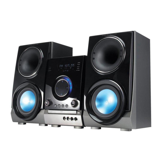
- Page 1 Internal Use Only Website http://biz.lgservice.com MICRO Hi-Fi SYSTEM SERVICE MANUAL MODEL: RBD154 (RBS154V) P/NO : AFN72956676 APRIL, 2009...
-
Page 2: Table Of Contents
[CONTENTS] ❍ SECTION 1. GENERAL • SERVICING PRECAUTIONS ..........1-2 •... -
Page 3: Section 1. General
SECTION 1. GENERAL SERVICING PRECAUTIONS NOTES REGARDING HANDLING OF THE PICK-UP 1. Notes for transport and storage 1) The pick-up should always be left in its conductive bag until immediately prior to use. 2) The pick-up should never be subjected to external pressure or impact. Storage in conductive bag Drop impact 2. - Page 4 NOTES REGARDING COMPACT DISC PLAYER REPAIRS 1. Preparations 1) Compact disc players incorporate a great many ICs as well as the pick-up (laser diode). These components are sensitive to, and easily affected by, static electricity. If such static electricity is high voltage, components can be damaged, and for that reason components should be handled with care.
-
Page 5: Esd Precautions
ESD PRECAUTIONS Electrostatically Sensitive Devices (ESD) Some semiconductor (solid state) devices can be damaged easily by static electricity. Such components commonly are called Electrostatically Sensitive Devices (ESD). Examples of typical ESD devices are integrated circuits and some field-effect transistors and semiconductor chip components. The following techniques should be used to help reduce the incidence of component damage caused by static electricity. -
Page 6: Service Information For Eeprom
SERVICE INFORMATION FOR EEPROM POWER ON FLD no disc status Remote control DETECT NEW EEPROM “pause →1→4→7→2” (OPTION EDIT SCREEN) NAME OPT 0 FLD ‘OP-0…. OPT 1 OPT 2 OPT 3 OPT 4 Move to appropriate position OPT 5 and make changes OPT 6 with Rmc ‘cursor,number’... -
Page 7: Program Download Guide
PROGRAM DOWNLOAD GUIDE 1. AUDIO PROGRAM Download program file name must be RBD154.HEX → If security program (Water Wall) is activated on your PC, you must save the file to the usb storage device and disable the security software, then download the file to your set. Caution: When downloading the file, you should neither unplug the usb device, change to the other function, nor power off the device. - Page 8 2. DVD PROGRAM Download program file name must be HB001_DATE_00.BIN → If security program (Water Wall) is activated on your PC, you must save the file to the usb storage device and disable the security software, then download the file to your set. Caution: When downloading the file, you should neither unplug the usb device, change to the other function, nor power off the device.
-
Page 9: Specifications
SPECIFICATIONS GENERAL Power supply Refer to main label. Power consumption Refer to main label. Net Weight 3.8 kg External dimensions (W x H x D) 202 x 307 x 262 mm Operating conditions Temperature 5°C to 35°C, Operation status: Horizontal Operating humidity 5% to 85% Laser... -
Page 10: Section 2. Exploded Views
SECTION 2. EXPLODED VIEWS • CABINET AND MAIN FRAME SECTION (RBD154) NOTES) THE EXCLAMATION POINT WITHIN AN EQUILATERAL TRIANGLE IS INTENDED TO ALERT THE SERVICE PERSONNEL TO THE PRESENCE OF IMPORTANT SAFETY INFORMATION IN SERVICE LITERATURE. A42 ASSY INCLUDES TOUCH PCB OPTIONAL PART CABLE1 KARAOKE... -
Page 11: Deck Mechanism Exploded View (Dp-12Av)
• DECK MECHANISM EXPLODED VIEW (DP-12AV) 015B 015A 012A... -
Page 12: Speaker Section
• SPEAKER SECTION 1. FRONT/REAR SPEAKER (RBS154V) A61B A61A... -
Page 13: Packing Accessory Section
• PACKING ACCESSORY SECTION 832 Disc 827 Micro Phone 801 Instruction Ass'y 808 Battery 825 FM Wire Antenna 811 Plug Ass'y, 1Way 900 Remote Control 803 Packing 804 Bag 802 Box... -
Page 14: Section 3. Electrical Part
SECTION 3. ELECTRICAL PART AUDIO ELECTRICAL TROUBLESHOOTIHG GUIDE 1. POWER (SMPS) POWER (SMPS) Check the fuse Replace the fuse F901 Check the DC V of C905 Check BD901, LF901, 902 if DC V is over 400V Check the DC V of C909,C903,C921 Check IC901, 902 Replace IC901, 902 If DC V is in 14~19V... - Page 15 2. P-SEN 3. VKK PART CHECK P-SENS VKK CHECK Check Check Check power circuit Check power circuit the pin3 of P9702 the pin6 of P9702 troubleshooting troubleshooting. if DC V is over if DC V is over 32V ±1 5.6V 4.
- Page 16 5. MICOM PART CHECK II MICOM PART CHECK II Refer to SMPS Check P7904 5pin 5.6V troubleshooting Check power Check D101 RS1G of both terminals of D101 output is working on 5V RS1G Replace the related parts Check the related part Check IC102 Check output power of IC101 Check IC102 1pin high...
- Page 17 6. IC103 S-24CS16A01 PART CHECK CHECK IC100 LC87F5NC8A 93, 94 PIN Refer to micom 93pin DATA 94pin CLK Check MICOM power 5V troubleshooting Check the related part Replace the related parts...
- Page 18 7. FLD DISPLAY PART CHECK FLD DISPLAY CHECK Check Refer to SMPS P7904 1,2,3 power troubleshooting F1+,F2-both terminals:over 4.4V Check power VKK:over -32V Check P7904 assembly Check P7904 connection Check condition and power F1+,F2- Replace the related part both terminals:over 4.4V power of each pin check power VKK:over 32V check 5pin:5.6V...
- Page 19 8. TOUCH-PAD PART CHECK TOUCH-PAD CHECK IC305 Refer to SMPS PN352 1pin 5V 28pin check 5V troubleshooting Check IC305 13pin, 11pin, Check resistance output of Replace the related part IC100 96pin:CLK, line CLK:R128 DATA:R126 95pin:DATA 9. PWM MODULATION PART CHECK PWM MODULATION PART CHECK Check...
- Page 20 Check IC604 PS9831 Replace the related part Check R666(1M) output 86pin CLK input Check output of IC100 Check LC87F5NC8A resistance output of line 87→PWM_CLK DATA:R103 Replace the related part CLK:R141 86→PWM_DATA RST:R152 34→PWM_REST Check IC604 Check DVD PS9831 data input ASS`Y PS9831 Refer to DVD troubleshooting 78 PIN→DATA...
- Page 21 10. PWM AMP PART CHECK POWER AMP PART CHECK P7905 Refer to SMPS troubleshooting 3pin + 13,14,15 pin 26V Check input power IC700 41, 35, 32, 26pin Check resistance power Check input power of IC700, IC700:R702,701,726,727,724 1, 44, 23, 22, 21pin +12V Check PWM modulator input 23, 26pin Check POWER IC700 34, 29pin output...
- Page 22 11. TUNER FUNCTION PART CHECK TUNER FUNCTION PART CHECK Check TUNER Check TUNER module power module(TU100) is working (check 4pin 9V) Check IC300(CS5346) 23, 24pin input waveform Check IC300(CS5346) Replace the related parts 41pin output waveform...
- Page 23 DVD ELECTRICAL TROUBLESHOOTIHG GUIDE 1. POWER PART CHECK GUIDE POWER ON Select the DVD mode Does it Does DVD Check an Audio micom appear DVD error at appear at FLD? FLD? Check connector (P7904, P7905) Reconnect Check the voltage of each Does no disc or pin on P7905 9,10pin time are appeared at...
- Page 24 2. TEST & DEBUG FLOW POWER ON Check connection lines between Flash memory FLASH & ES8391 or the FLASH Show LOGO? operates properly? access time whether is suitable or not Check connection lines SDRAM works between SDRAM (IC502) & properly? ES8391 or the SDRAM is damaged Check the related circuit of...
- Page 25 Does the Motor driver SLED move to inner side Check the MD DRV_MMUTE pin when it is at outer position? high 3 Check the related circuit of SLED SLED signal is ok? and Motor driver IC (IC401) Do not put in disc Check the cable connection and tray close with MECHA...
- Page 26 Laser turns on Check the laser power circuit between DVDLD or CDLD when reading ES8391 and power transistor output properly? disc? (Q405, Q406) Collector Check the related circuit of laser voltage of power transistor power transistor is ok? (Q405, Q406) Check cable connection between P405 and pick-up head Put disc in tray...
- Page 27 Check the connections between Proper signal on Focus on ok? P405 and pick-up head A,B,C,D from MD? Check the related circuit of Proper FOD signal on ES8391 focus signal IC401? Check cable connection between P405 and MD Check the related circuit Proper TRD signal on Tracking ok? between IC401 and ES8391...
- Page 28 outputs are ok Check the connections Audio signal data on during playing between ES8391 P8391 is ok? disk? Check the main pcb For example composite video, Picture check the video mute signal data on TEST END TR (Q506), ES8391 ES8391 is ok? video signal data.
- Page 29 3. USB PART TURN ON USB "Searching" or Check the power supply circuit "USB" display check (Check CN201) Check the HRST#signal Check the HRST#signal check the usb part and dvd part line Check the usb jack power supply Reading ok check (Check CN201) Check the usb data line (CN201)
-
Page 30: Details And Waveforms On System Test And Debugging
DETAILS AND WAVEFORMS ON SYSTEM TEST AND DEBUGGING 1. WHEN POWER ON, RESET & DATA ETC WAVEFORM SPI DI IC501 pin 56 SPI DO IC501 pin 57 IC501 pin 59 SPDIF-OUT SPI-CS3 IC503 pin 1 HRST# USB_N1 IC501 pin 111 USB_P1 IC501 pin 110 3-17... - Page 31 2. OPEN/CLOSE WAVEFORM AT POWER ON Open IC401 pin 11 Open_sw IC501 pin 60 Close_sw IC501 pin 63 Close IC401 pin 10 3. STARTING ACTION WAVEFORM IN MD DEVICE Driver STBY SLEGN IC401 pin 18 IC401 pin 17 4. FOCUS WAVEFORM (AT CD) IC401 pin 3 IC401 pin 4 3-18...
- Page 32 5. FOCUS WAVEFORM (AT DVD) Q405(DVD_LD) Q405 Q406(CD_LD) Q406 6. AT POWER ON , SPINDLE SIGNAL AT MD DECK SPINDELD IC401 pin 21 SPIN+ IC401 pin 15 SPIN- IC401 pin 16 7. TRACKING SIGNAL IC401 pin 7 IC401 pin 2 IC401 pin 1 3-19...
- Page 33 8. RF WAVEFORM 9. DISK TYPE JUGEMENT WAVEFORM IC401 pin 3 IC401 pin 6 SVREF IC401 pin 23 IC401 pin 3 IC401 pin 6 SVREF IC401 pin 23 3-20...
-
Page 34: Wiring Diagram
WIRING DIAGRAM TUNER MODULE 3-21... -
Page 35: Block Diagrams
BLOCK DIAGRAMS 1. MAIN BLOCK DIAGRAM 3-22... - Page 36 2. SMPS BLOCK DIAGRAM 3-23...
- Page 37 3-24...
-
Page 38: Circuit Diagrams
FROM THE ACTUAL CIRCUIT USED. THIS WAY, 2. Voltages are DC-measured with a digital voltmeter BE MODIFIED OR ALTERED WITHOUT PERMISSION IMPLEMENTATION OF THE LATEST SAFETY AND during Play mode. FROM THE LG CORPORATION. ALL COMPONENTS PERFORMANCE IMPROVEMENT CHANGES INTO... - Page 39 2. MICOM CIRCUIT DIAGRAM MICOM RBD154 EBY58534601_1 2009. 02. 13 3-27 3-28...
- Page 40 3. DSP & PWM CIRCUIT DIAGRAM DSP+PWM RBD154 EBY58534601_2 2009. 02. 13 3-29 5-30...
- Page 41 4. AMP CIRCUIT DIAGRAM RBD154 EBY58534601_3 2009. 02. 13 3-31 3-32...
- Page 42 5. MPEG CIRCUIT DIAGRAM MPEG RBD154 EBY58534601_4 WAVEFORM 2009. 02. 13 3-33 3-34...
- Page 43 6. SERVO CIRCUIT DIAGRAM SERVO RBD154 EBY58534601_5 WAVEFORM 2009. 02. 13 3-35 3-36...
- Page 44 7. I/O CIRCUIT DIAGRAM RBD154 EBY58534601_6 2009. 02. 13 3-37 3-38...
- Page 45 8. HDMI CIRCUIT DIAGRAM HDMI RBD154 EBY58534601_7 2009. 02. 13 3-39 3-40...
- Page 46 9. FRONT CIRCUIT DIAGRAM FRONT RBD154 EBY58534701 2009. 02. 13 3-41 3-42...
- Page 47 10. KARAOKE + USB CIRCUIT DIAGRAM KARAOKE+USB RBD154 EBY58535901 2009. 02. 13 3-43 3-44...
- Page 48 11. MIC/HEAD PHONE/PORTABLE CIRCUIT DIAGRAM MIC/HEAD PHONE/PORTABLE RBD154 EBY58536101 2009. 02. 13 3-45 3-46...
- Page 49 12. SCART CIRCUIT DIAGRAM SCART RBD154 EBY58536201 2009. 02. 13 3-47 3-48...
- Page 50 13. TOUCH KEY CIRCUIT DIAGRAM TOUCH KEY RBD154 EBY58536301 2009. 02. 13 3-49 3-50...
-
Page 51: Circuit Voltage Chart
CIRCUIT VOLTAGE CHART VOLT VOLT VOLT VOLT VOLT VOLT VOLT VOLT IC100(MICOM 0.77 1.64 0.96 LC87F54CN8A) 5.12 0.75 0.96 0.05 5.08 IC202(MC4580) 0.73 2.95 0.96 3.34 5.06 0.06 0.43 1.26 0.96 3.32 3.48 0.05 0.06 2.08 0.96 1.08 0.02 1.54 0.96 3.32 5.09... - Page 52 VOLT VOLT VOLT VOLT VOLT VOLT 1.55 0.06 1.55 0.14 3.06 4.01 3.42 3.06 3.32 3.35 3.31 3.32 IC505(74LV132PW) 3.43 3.24 1.24 3.24 0.25 3.38 3.31 1.55 3.42 3.24 3.31 3.31 0.86 1.16 3.31 3.34 1.67 1.13 1.12 3.42 3.35 3.31 IC805(ES7108) 0.84...
-
Page 53: Printed Circuit Diargams
PRINTED CIRCUIT BOARD DIARGAMS 1. MAIN P.C. BOARD DIAGRAM ( TOP VIEW ) 3-55 3-56... - Page 54 MAIN P.C. BOARD DIAGRAM ( BOTTOM VIEW ) 3-57 3-58...
- Page 55 2. SMPS P.C. BOARD DIAGRAM NOTE: Warning Parts that are shaded are critical With respect to risk of fire or electrical shock. 3-59 3-60...
- Page 56 3. FRONT P.C. BOARD DIAGRAM 3-61 3-62...
- Page 57 4. TOUCH PAD P.C. BOARD DIAGRAM ( TOP VIEW ) TOUCH PAD P.C. BOARD DIAGRAM ( BOTTOM VIEW ) 5. USB/MIC P.C. BOARD DIAGRAM 6. SCART P.C. BOARD DIAGRAM ( TOP VIEW ) SCART P.C. BOARD DIAGRAM ( BOTTOM VIEW ) 3-63 3-64...
-
Page 58: Section 4. Mechanism (Dp-12Av)
SECTION 4. MECHANISM (DP-12AV) [CONTENTS] DECK MECHANISM PARTS LOCATIONS • Top View ............. . . 4-2 •... -
Page 59: Deck Mechanism Parts Locations
DECK MECHANISM PARTS LOCATIONS • Top View Procedure Fig- Disasse Parts Fixing Type mbly Starting No. Main Base Clamp Assembly Disc 1, 2 Plate Clamp 1, 2, 3 Magnet Clamp 1, 2, 3, 4 Clamp Upper Tray Disc 1, 6 Base Assembly Sled 1, 2, 6 Gear Feed... -
Page 60: Deck Mechanism Disassembly
DECK MECHANISM DISASSEMBLY TRAY DISC MAIN BASE DISC CLAMP ASSEMBLY PLATE CLAMP MAGNET CLAMP CLAMP UPPER (Fig. A) BASE MAIN HOLDER LEVER BASE MAIN BASE MAIN BOTTOM SIDE VIEW Fig. 4-1 Fig. 4-2 1. Main Base (Fig. 4-1) 2. Tray Disc (Fig. 4-2) 1) Insert and push a Driver in the emergency eject 1-1. -
Page 61: Base Assembly Sled
RUBBER DAMPER Distinguish upper and lower sides (Assemble with care) RUBBER DAMPER Distinguish upper and lower sides RUBBER DAMPER (Assemble with care) BASE PU (S2) (S2) RUBBER DAMPER GENERAL PICK UP ASSEMBLY GEAR RACK SPINDLE MOTOR ASSEMBLY Fig. 4-3 3. Base Assembly Sled (Fig. 4-3) 3-3. -
Page 62: Frame Assembly Up/Down
GUIDE UP/DOWN GEAR LOADING GEAR PULLEY (L6) SCREW INSERTION (L6) TORGUE CONTROL BASE MAIN (L4) BELT LOADING (H1) (C2) PWB ASSEMBLY LOADING (S5) (S4) BASE MAIN (S4) UP/DOWN FRAME ASSEMBLY (L5) GUIDE UP/DOWN FIG. (A) FIG. (B) GUIDE UP/DOWN GUIDE UP/DOWN FIG. -
Page 63: Deck Mechanism Exploded View (Dp-12Av)
DECK MECHANISM EXPLODED VIEW (DP-12AV) 015B 015A 012A...