Philips FWM462 Service Manual
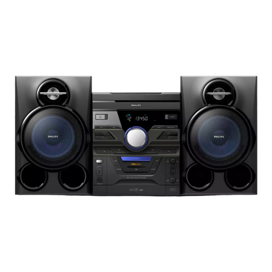
280w mini hi-fi system
Hide thumbs
Also See for FWM462:
- Service manual (31 pages) ,
- User manual (23 pages) ,
- Quick start manual (2 pages)
Quick Links
See also:
User Manual
280W Mini Hi-Fi System
CONTENTS
Technical specification ..................................................................1-2
Version variation ...........................................................................1-2
Service measurement setup..........................................................1-3
Service aids .................................................................................1-4
Instructions on CD playability ................................................2-1..2-2
Block diagram ................................................................................3-1
Wiring diagram ..............................................................................4-1
Disassembly diagram............ ................................................5-1..5-2
Main board
Circuit diagram .........................................................................6-1
Layout diagram ..................................................................6-2..6-3
AC board
Circuit diagram .........................................................................7-1
Layout diagram ..................................................................7-2..7-3
Display board
Circuit diagram .........................................................................8-1
Layout diagram ..................................................................8-2..8-3
©
Copyright 2010 Philips Consumer Electronics B.V. Eindhoven, The Netherlands
All rights reserved. No part of this publication may be reproduced, stored in a retrieval
system or transmitted, in any form or by any means, electronic, mechanical, photocopying,
or otherwise without the prior permission of Philips.
Published by LX 1023 Service Audio
Version 1.0
Subject to modification
AMP & Power Board
Circuit diagram. ........................................................................9-1
Layout diagram ..................................................................9-2..9-3
Tuner board
Circuit diagram .......................................................................10-1
Layout diagram .......................................................................10-2
CD Board
Circuit diagram. ...................................................................... 11-1
Layout diagram .............................................................. 11-2..11-3
MCU Board
Circuit diagram. .............................................................12-1..12-2
Layout diagram ..............................................................12-3..12-4
Exploded view diagram ...............................................................13-1
FWM462
-/55/77/BK
3141 785 35290

Related Manuals for Philips FWM462


Summary of Contents for Philips FWM462
- Page 1 Layout diagram ..............8-2..8-3 © Copyright 2010 Philips Consumer Electronics B.V. Eindhoven, The Netherlands All rights reserved. No part of this publication may be reproduced, stored in a retrieval system or transmitted, in any form or by any means, electronic, mechanical, photocopying, or otherwise without the prior permission of Philips.
-
Page 2: Technical Specification
• Station presets: 40 • Tuner Bands: MW, FM Stereo • Power supply: 100-240VAC, 50/60Hz • Tuner Enhancements: Auto Store, Easy Set (Plug & • Play) VERSION VARIATION FWM462 Type /Versions: Service policy Board in used: AC BOARD MAIN BOARD TUNER BOARD AMP &... -
Page 3: Measurement Setup
MEASUREMENT SETUP Tuner FM Bandpass LF Voltmeter 250Hz-15kHz e.g. PM2534 e.g. 7122 707 48001 RF Generator e.g. PM5326 S/N and distortion meter e.g. Sound Technology ST1700B Use a bandpass filter to eliminate hum (50Hz, 100Hz) and disturbance from the pilottone (19kHz, 38kHz). Tuner AM (MW,LW) Bandpass LF Voltmeter... -
Page 4: Service Aids
SERVICE AIDS WARNING All ICs and many other semi-conductors are susceptible to electrostatic discharges (ESD). Careless handling during repair can reduce life drastically. When repairing, make sure that you are connected with the same potential as the mass of the set via a wrist wrap with resistance. Keep components and tools also at this potential. - Page 5 2 - 1 INSTRUCTIONS ON CD PLAYABILITY Customer complaint "CD related problem" Set remains closed! check playability playability ok ? For flap loaders (= access to CD drive possible) "fast" lens cleaning cleaning method is recommended check playability playability ok ? Play a CD for at least 10 minutes check playability...
- Page 6 2 - 2 INSTRUCTIONS ON CD PLAYABILITY PLAYABILITY CHECK LIQUID LENS CLEANING Before touching the lens it is advised to clean the surface of the lens by blowing clean air over it. For sets which are compatible with CD-RW discs This to avoid that little particles make scratches on use CD-RW Printed Audio Disc ....7104 099 96611 the lens.
-
Page 7: Block Diagram
BLOCK DIAGRAM TUNER ET8862& SI4730 KEY PART 3CD LOADER 3CDC MOTOR DRIVER DRIVER IC BA5826 FAN8100N PICK UP CONTROL DATA MOTOR 8M SERIAL MOTOR FALSH SST29VF080B CD SERVO BU9543 BX8800 16M SDRAM 128pin QFP CD PCM BCK,LRCK, DATE USB/SD BCK,LRCK 74LVC157 WM8782 ,DATE... -
Page 8: Wiring Diagram
WIRING DIAGRAM KEY1 BOARD MCU BOARD DISPLAY BOARD CD BOARD MAIN BOARD AMP BOARD AC BOARD... - Page 11 R620 NJM4556AM LEFT C608 1UF R6612K2 330N BAS316 D606 AUX601 R635 C648 100P Z602 MUTE C655 100U C613 6V2(6v8 FOR FWM462) C609 100P R686 1M AMP_ALC R618 LIN-R D604 RIGHT C653 33P C658 C667 R619 BAS316 LIN-L R610 100P 0.47U...
-
Page 12: Layout Diagram
LAYOUT DIAGRAM - MAIN BOARD TOP SIDE... - Page 13 LAYOUT DIAGRAM - MAIN BOARD BOTTOM SIDE...
- Page 14 CIRCUIT DIAGRAM - AC BOARD D815 1N5402 C806 C802 C803 0.02U 3300UF/50V CON801 D817 1N5402 R801 10K +32V C826 0.02U R836 D816 1N5402 T801 C804 0.02U F805 -32V ONLY FOR ECO FWM452/55 D818 1N5402 C828 C821 T5A L 250V 3300UF/50V C827 0.02U D835 1N5392...
- Page 15 PCB LAYOUT - AC BOARD...
- Page 16 CIRCUIT DIAGRAM - DISPLAY BOARD KEY1 C9065 4N7 C9013 R9023 10K 0.47/50V C9017 MIC-OUT R9026 SW901 C9009 470N 10U/16V SW911 R9007 SW921 VCC10V CN908 R9011 VR901 STOP C9014 R9025 DISPAY Q971 R9009 50K x2 100P C9007 BC857B 330K AGND L9005 L9001 SW902 SW912...
- Page 17 LAYOUT DIAGRAM - DISPLAY BOARD TOP SIDE...
- Page 18 LAYOUT DIAGRAM - DISPLAY BOARD BOTTOM SIDE...
- Page 19 CIRCUIT DIAGRAM - AMP BOARD STK433-870(ZIP23) FOR FWM452 U701 STK433-090 FOR FWM462 C763 100N R725 C701 470N L703 11T5 R762 C702 470N C746 100P R798 R705 R728 R706 C747 C739 R746 R736 R771 C721 C711 C719 C737 470N RIGHT(HIGHT) R777...
- Page 20 PCB LAYOUT - AMP BOARD TOP SIDE...
- Page 21 PCB LAYOUT - AMP BOARD BOTTOM SIDE...
- Page 22 10-1 10-1 CIRCUIT DIAGRAM - TUNER BOARD...
- Page 23 10-2 10 - 2 LAYOUT DIAGRAM - TUNER BOARD...
- Page 24 11-1 11-1 CIRCUIT DIAGRAM-CD BOARD...
- Page 25 11-2 11-2 LAYOUT DIAGRAM-CD BOARD TOP SIDE...
- Page 26 11-3 11-3 LAYOUT DIAGRAM-CD BOARD BOTTOM SIDE...
- Page 27 12-1 12-1 CIRCUIT DIAGRAM - MCU BOARD PART1 R103 place GND Arround Track M40 R116 Close pin52 PWR_DET R143 C156 TU_SCLK C157 TU_SCLK TU-SDA L109 470R C159 C158 C177 C155 IC102 IC104 AD5/EAD5 VDD1 VSS6 DQ15 +3V3 GP03 3CD1_SW AD4/EAD4 DQ14 +3V3 GP04...
- Page 28 12-2 12-2 CIRCUIT DIAGRAM - MCU BOARD PART2 R533 C536 3U3/50v CD-R This GND R535 2K2 must be C520 100n C532 use AGND C533 R536 470P 470P C519 100u/16v R531 2K2 CD+8V C531 R537 470P C534 C518 100n 470P R534 CD-L CD-L CD-L...
- Page 29 12-3 12-3 PCB LAYOUT - MCU BOARD TOP SIDE...
- Page 30 12-4 12-4 PCB LAYOUT - MCU BOARD BOTTOM SIDE...
- Page 31 13-1 13-1 SET EXPLODED VIEW...