Sony CDX-H910UI Service Manual
Fm/am compact disc player
Hide thumbs
Also See for CDX-H910UI:
- Operating instructions manual (132 pages) ,
- Specifications (2 pages) ,
- Installation/connections (2 pages)
Table of Contents
Quick Links
CDX-H910UI/HR910UI
SERVICE MANUAL
Ver. 1.0 2008.12
• The tuner and CD sections have no adjustments.
AUDIO POWER SPECIFICATIONS (CDX-H910UI only)
CEA2006 Standard
Power Output: 17 Watts RMS × 4 at 4 Ohms < 1% THD+N
SN Ratio: 82 dBA (reference: 1 Watt into 4 Ohms)
CD Player section
Signal-to-noise ratio: 120 dB
Frequency response: 10 – 20,000 Hz
Wow and fl utter: Below measurable limit
Tuner section
CDX-H910UI:
FM
Tuning range:
87.5 – 108.0 MHz (at 50 kHz step)
87.5 – 107.9 MHz (at 200 kHz step)
FM tuning interval:
50 kHz/200 kHz switchable
Antenna (aerial) terminal:
External antenna (aerial) connector
Intermediate frequency: 150 kHz
Usable sensitivity: 10 dBf
Selectivity: 75 dB at 400 kHz
Signal-to-noise ratio: 70 dB (mono)
Separation: 40 dB at 1 kHz
Frequency response: 20 – 15,000 Hz
AM
Tuning range:
531 – 1,602 kHz (at 9 kHz step)
530 – 1,710 kHz (at 10 kHz step)
AM tuning interval: 9kHz/10kHz switchable
Antenna (aerial) terminal:
External antenna (aerial) connector
Intermediate frequency: 25 kHz
Sensitivity: 26 μV
Sony Corporation
9-889-372-01
2008L04-1
Audio&Video Business Group
©
2008.12
Published by Sony Techno Create Corporation
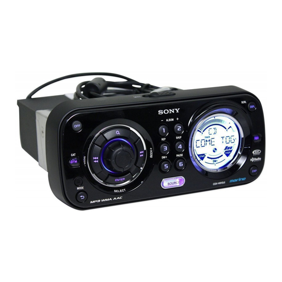
(Photo: CDX-HR910UI)
Model Name Using Similar Mechanism
CD Drive Mechanism Type
Optical Pick-up Name
SPECIFICATIONS
CDX-HR910UI:
FM
Tuning range: 87.5 – 108.0 MHz
Antenna (aerial) terminal:
External antenna (aerial) connector
Intermediate frequency: 150 kHz
Usable sensitivity: 10 dBf
Selectivity: 75 dB at 400 kHz
Signal-to-noise ratio: 70 dB (mono)
Separation: 40 dB at 1 kHz
Frequency response: 20 – 15,000 Hz
MW/LW
Tuning range:
MW: 531 – 1,602 kHz
LW: 153 – 279 kHz
Antenna (aerial) terminal:
External antenna (aerial) connector
Intermediate frequency: 25 kHz
Sensitivity: MW: 26 μV, LW: 45 μV
USB Player section
Interface: USB (Full-speed)
Maximum current: 500mA
FM/AM COMPACT DISC PLAYER
FM/MW/LW COMPACT DISC PLAYER
US Model
Canadian Model
CDX-H910UI
AEP Model
UK Model
CDX-HR910UI
E Model
CDX-H910UI
CDX-GT930UI/GT937UI/
GT980UI
MG-101Z-188//Q
DAX-25A
Power amplifi er section
Outputs: Speaker outputs (sure seal connectors)
Speaker impedance: 4 – 8 ohms
Maximum power output: 52 W × 4 (at 4 ohms)
General
Outputs:
Audio outputs terminal (front/rear)
Subwoofer output terminal (mono)
Power antenna (aerial) relay control terminal
Power amplifi er control terminal
Inputs:
Remote controller input terminal
Antenna (aerial) input terminal
Telephone ATT control terminal
Illumination control terminal
BUS control input terminal
BUS audio input terminal
AUX input terminal
USB signal input terminal
– Continued on next page –
CDX-H910UI
CDX-HR910UI
Table of Contents

Related Manuals for Sony CDX-H910UI


Summary of Contents for Sony CDX-H910UI
- Page 1 • The tuner and CD sections have no adjustments. CDX-GT930UI/GT937UI/ Model Name Using Similar Mechanism GT980UI AUDIO POWER SPECIFICATIONS (CDX-H910UI only) CD Drive Mechanism Type MG-101Z-188//Q CEA2006 Standard Power Output: 17 Watts RMS × 4 at 4 Ohms < 1% THD+N...
- Page 2 THESE COMPONENTS WITH SONY PARTS PAR DES PIÈCES SONY DONT LES NUMÉROS SONT DON- WHOSE PART NUMBERS APPEAR AS SHOWN IN THIS NÉS DANS CE MANUEL OU DANS LES SUPPLÉMENTS MANUAL OR IN SUPPLEMENTS PUBLISHED BY SONY. PUBLIÉS PAR SONY.
-
Page 3: Table Of Contents
R/CD-RW (MP3/WMA/AAC fi les). SERVICING NOTES ..........Type of discs Label on the disc GENERAL Location of Controls (CDX-H910UI) ......CD-DA Location of Controls (CDX-HR910UI) ......Connection Example (CDX-H910UI) ......Connection Example (CDX-HR910UI) ......Connections (CDX-H910UI) .......... Connections (CDX-HR910UI) ........ -
Page 4: Servicing Notes
CDX-H910UI/HR910UI SECTION 1 SERVICING NOTES EXTENSION CABLE AND SERVICE POSITION When repairing or servicing this set, connect the jig (extension cable) as shown below. • Connect the MAIN board (CN201) and the SERVO board (CN401) with the extension cable (Part No. J-2502-076-1). -
Page 5: General
CDX-H910UI/HR910UI SECTION 2 GENERAL This section is extracted from instruction manual. • LOCATION OF CONTROLS (CDX-H910UI) Location of controls and basic operations Main unit This section contains instructions on the location (BACK)/MODE button page 11, 12, of controls and basic operations. For details, see the respective pages. -
Page 6: Location Of Controls (Cdx-Hr910Ui)
CDX-H910UI/HR910UI • LOCATION OF CONTROLS (CDX-HR910UI) Location of controls and basic operations Main unit This section contains instructions on the location (BACK)/MODE button page 11, 12, of controls and basic operations. For details, see the respective pages. Press to: Return to the previous display/... -
Page 7: Connection Example (Cdx-H910Ui)
CDX-H910UI/HR910UI • CONNECTION EXAMPLE (CDX-H910UI) Connection example Anschlussbeispiel Notes ( - A ) Hinweise ( - A ) • Be sure to connect the ground (earth) lead before connecting • Schließen Sie unbedingt zuerst das Massekabel an, bevor Sie the amplifier. -
Page 8: Connections (Cdx-H910Ui)
CDX-H910UI/HR910UI • CONNECTIONS (CDX-H910UI) Supplied with XA-C40 Fourni avec le XA-C40 Suministrado con el XA-C40 Source selector Mit dem XA-C40 geliefert (not supplied) Geleverd met de XA-C40 Sélecteur de source (non fourni) Selector de fuente Supplied with the CD changer... -
Page 9: Connections (Cdx-Hr910Ui)
CDX-H910UI/HR910UI • CONNECTIONS (CDX-HR910UI) Supplied with XA-C40 Fourni avec le XA-C40 Suministrado con el XA-C40 Source selector Mit dem XA-C40 geliefert (not supplied) Geleverd met de XA-C40 Sélecteur de source In dotazione con il modello XA-C40 (non fourni) Selector de fuente... -
Page 10: Disassembly
CDX-H910UI/HR910UI SECTION 3 DISASSEMBLY • This set can be disassembled in the order shown below. 3-5. SERVO BOARD (Page 12) 3-1. FRONT PANEL OVERALL ASSY (Page 10) 3-6. CHASSIS (T) SUB ASSY (Page 13) 3-2. SUB PANEL SECTION (Page 11) 3-7. -
Page 11: Sub Panel Section
CDX-H910UI/HR910UI 3-2. SUB PANEL SECTION seal (base) two screws (+K (5 × 8)) two screws (+K (5 × 8)) two screws (+PTT 2.6 × 6) CN802 sub panel section 3-3. CD MECHANISM BLOCK sheet (chassis) screw two screws (+PTT 2.6 × 6) (+PTT 2.6 ×... -
Page 12: Main Board
CDX-H910UI/HR910UI 3-4. MAIN BOARD screw automobile cord (USB) screw (+PTT 2.6 × 8) (+PTT 2.6 × 8) screw (+PTT 2.6 × 10) two screws (+P 2.6 × 8) two screws CN203 (5P) (+PTT 2.6 × 12) cord (RCA) three ground point screws two screws (+PTT 2.6 ×... -
Page 13: Chassis (T) Sub Assy
CDX-H910UI/HR910UI 3-6. CHASSIS (T) SUB ASSY two screws two screws (M 1.7 × 2.5) (M 1.7 × 2.5) chassis (T) sub assy claw 3-7. ROLLER ARM ASSY roller arm assy gear (RA1) spring (RAL) washer spring (RAR) -
Page 14: Chassis (Op) Assy
CDX-H910UI/HR910UI 3-8. CHASSIS (OP) ASSY chassis (OP) assy tension spring (KF) two coil springs (damper) (natural) coil spring (damper) (green) slider (R) lever (D) gear (LE1) 3-9. CHUCKING ARM SUB ASSY chucking arm sub assy spring Note: Have this portion receive the chassis. -
Page 15: 3-10. Sled Motor Assy
CDX-H910UI/HR910UI 3-10. SLED MOTOR ASSY three serration screws (M 2 × 3) sled motor assy spring turn table spring stand Note: Never remove these parts since they were adjusted. stand Note: Place the stand with care not to touch the turn table. -
Page 16: 3-11. Optical Pick-Up Section
CDX-H910UI/HR910UI 3-11. OPTICAL PICK-UP SECTION optical pick-up section Note: Be careful not to touch the lens and hologram terminal when removing the optical pick-up section. 3-12. OPTICAL PICK-UP tapping screw (P 1.4) leaf spring (OPS) rack optical pick-up lead screw assy... -
Page 17: Diagrams
CDX-H910UI/HR910UI SECTION 4 DIAGRAMS THIS NOTE IS COMMON FOR PRINTED WIRING BOARDS AND SCHEMATIC DIAGRAMS. • Waveforms (In addition to this, the necessary note is printed in each block.) – MAIN Board – For Printed Wiring Boards. For Schematic Diagrams. -
Page 18: Block Diagram -Main Section
CDX-H910UI/HR910UI 4-1. BLOCK DIAGRAM – MAIN Section – J901 (1/2) INPUT SELECT/ ELECTRONIC VOLUME IC401 J901 (2/2) AUDIO BUS-RCH OUT_RLCH AUDIO OUT BUS_LCH OUT_RRCH R-CH REAR MUTE R-CH (REAR) BUS-RCH BUS_RCH (REAR) Q903 AU_LCH CD_LCH OUT_FLCH AUDIO OUT CD-RCH CD-RCH... -
Page 19: Block Diagram -Display Section
CDX-H910UI/HR910UI 4-2. BLOCK DIAGRAM – DISPLAY Section – SYSTEM CONTROL IC501 (2/2) RC_IN1 LCD_CE 48 LCD_CE J701 LCD_DATA RC_IN0 LCD_SO 49 (REMOTE IN) KEY_ACK0 LCD_SCK 50 LCD_CLK SIRCS 95 SIRCS OSC_OUT FRONT X501 PANEL 7.92MHz UNIT RE_IN1 12 RE_IN1 OSC_IN... -
Page 20: Printed Wiring Board -Main Section
CDX-H910UI/HR910UI 4-3. PRINTED WIRING BOARD – MAIN Section – • : Uses unleaded solder. J901 AUDIO OUT AUDIO (MONO) REAR FRONT J701 (ANTENNA) (REMOTE IN) J601 (BUS CONTROL IN) C304 JW157 L702 C305 JW161 C306 C307 C302 C333 JW100 R921... -
Page 21: Schematic Diagram -Main Section (1/3)
CDX-H910UI/HR910UI 4-4. SCHEMATIC DIAGRAM – MAIN Section (1/3) – • See page 26 for IC Block Diagrams. IC301 TDA8588AJ/N2/R1 (H910UI) TDA8588AJ/N2/R1/M5 (HR910UI) IC301 POWER AMP/MULTIPLE REGULATOR MAIN BOARD (1/3) IC B/D CN701 H910UI FRONT L-CH REAR AMP-REM L-CH C314 C318 ANT-REM 0.01... -
Page 22: Schematic Diagram -Main Section (2/3)
CDX-H910UI/HR910UI 4-5. SCHEMATIC DIAGRAM – MAIN Section (2/3) – • See page 17 for waveforms. • See page 26, 27 for IC Block Diagrams. (2/3) MAIN BOARD IC401 IC B/D Q901-905 MUTE INPUT SELECT,ELECTRONIC VOLUME CN901 SUB_OUT SUB OUT MAIN... -
Page 23: Schematic Diagram -Main Section (3/3)
CDX-H910UI/HR910UI 4-6. SCHEMATIC DIAGRAM – MAIN Section (3/3) – • See page 17 for waveforms. • See page 28 for IC Block Diagrams. • See page 29 for IC Pin Function Description of IC501. (Page 21) MAIN BOARD (1/3) MAIN BOARD (3/3) -
Page 24: Printed Wiring Board -Sub Section
CDX-H910UI/HR910UI 4-7. PRINTED WIRING BOARD – SUB Section – • : Uses unleaded solder. CN801 1-871-923- (21) (Page 20) FRONT PANEL UNIT MAIN BOARD CN902 CN802 S802 PANEL OPEN DETECT R802 FB801 1-871-923- (21) CDX-H910UI/HR910UI... -
Page 25: Schematic Diagram -Sub Section
CDX-H910UI/HR910UI 4-8. SCHEMATIC DIAGRAM – SUB Section – CN801 FB801 CN802 R801 R802 S802 (Page 22) LSW801(1/2) C802 CDX-H910UI/HR910UI... - Page 26 CDX-H910UI/HR910UI • IC Block Diagrams IC301 TDA8588AJ/N2/R1/M5 (HR910UI) (MAIN Board (1/3)) IC601 BA8271F-E2 (MAIN Board (1/3)) IC401 BD3447FV-E2 (MAIN Board (2/3)) IC301 TDA8588AJ/N2/R1 (H910UI) (MAIN Board (1/3)) BUS ON BUS_ON SWITCH I2C_SIO RESET OUT–FL– C BUS SWITCH BUS_IN I2C_SCK CLK_IN...
- Page 27 CDX-H910UI/HR910UI IC1 TEF6607T/V4/S470/M5,518 (HR910UI) (MAIN Board (2/3)) IC1 TEF6607T/V4/S470,518 (H910UI) (MAIN Board (2/3)) AMRFIN 1 AMSELOUT2 AMSELOUT1 AMRFDEC 2 TUNER AMIFAGC1 FMIN2 3 AMSELIN2 TUNER FMIN1 4 AMSELIN1 GNDRF 5 VCC2 6 TEST PLLREF AMRFAGC 7 TUNING LOUT 8 STEREO DECODER...
- Page 28 CDX-H910UI/HR910UI IC801 TPS40200DRG4 (MAIN Board (3/3)) UVLO DRIVER ISNS 700mV LOGIC E/A and SS REFERENCE SOFT-START OVERCURRENT ENABLE E/A COMP IC802 TPS2051BDRG4 (MAIN Board (3/3)) CHARGE PUMP CURRENT DRIVER LIMIT UVLO THERMAL SENCE IC803 TC7WH123FU(TE12R) (MAIN Board (3/3)) 8 VCC...
- Page 29 CDX-H910UI/HR910UI • IC Pin Function Description MAIN BOARD (3/3) IC501 MB90F883AHPF-G-104E1 (SYSTEM CONTROL) Pin No. Pin Name Description CYRIL_SEL Cyrillic setting terminal “H”: Cyrillic ON, “L”: Cyrillic OFF B-OUT_SEL Black out setting terminal “H”: Block out ON, “L”: Block out OFF...
- Page 30 CDX-H910UI/HR910UI Pin No. Pin Name Description WAKE_UP CD mechanism servo wake up signal output MC_RX CD servo control serial data signal input MC_TX CD servo control serial data signal output CD servo control serial clock signal output Not used Z_MUTE...
-
Page 31: Exploded Views
CDX-H910UI/HR910UI SECTION 5 EXPLODED VIEWS Note: • -XX and -X mean standardized parts, so • Color Indication of Appearance Parts Ex- The components identifi ed by mark 0 they may have some difference from the ample: or dotted line with mark 0 are critical for original one. -
Page 32: Sub Panel Section
CDX-H910UI/HR910UI 5-2. SUB PANEL SECTION not supplied not supplied (SUB board) not supplied not supplied not supplied Ref. No. Part No. Description Remark Ref. No. Part No. Description Remark 2-696-239-01 PLATE (PANEL), HINGE 2-696-240-11 SEAL (BASE) 2-889-258-01 SCREW, +B M2 EG GRIP... -
Page 33: Main Section
CDX-H910UI/HR910UI 5-3. MAIN SECTION not supplied not supplied not supplied MG-101Z-188//Q FU601 not supplied not supplied not supplied not supplied Ref. No. Part No. Description Remark Ref. No. Part No. Description Remark A-1609-816-A MAIN BOARD, COMPLETE (H910UI) 3-264-798-01 A-1609-894-A MAIN BOARD, COMPLETE (HR910UI) -
Page 34: Cd Mechanism Section (Mg-101Z-188//Q)
CDX-H910UI/HR910UI 5-4. CD MECHANISM SECTION (MG-101Z-188//Q) not supplied not supplied not supplied not supplied not supplied not supplied not supplied not supplied not supplied not supplied not supplied not supplied Ref. No. Part No. Description Remark Ref. No. Part No. -
Page 35: Electrical Parts List
CDX-H910UI/HR910UI SECTION 6 MAIN ELECTRICAL PARTS LIST Note: • Due to standardization, replacements in • RESISTORS When indicating parts by reference num- the parts list may be different from the All resistors are in ohms. ber, please include the board name. - Page 36 CDX-H910UI/HR910UI MAIN Ref. No. Part No. Description Remark Ref. No. Part No. Description Remark C324 1-162-970-11 CERAMIC CHIP 0.01uF C809 1-162-917-11 CERAMIC CHIP 15PF C325 1-126-926-11 ELECT 1000uF C810 1-107-826-11 CERAMIC CHIP 0.1uF C328 1-128-057-11 ELECT 330uF 6.3V C813 1-126-924-11...
- Page 37 CDX-H910UI/HR910UI MAIN Ref. No. Part No. Description Remark Ref. No. Part No. Description Remark D504 6-500-334-01 DIODE MC2836-T112-1 < JACK > D505 6-501-193-01 DIODE 1SS355WTE-17 D601 6-501-782-01 DIODE MAZ8180GMLS0 1-815-185-13 JACK (ANTENNA) D603 6-501-782-01 DIODE MAZ8180GMLS0 J601 1-580-907-41 PLUG, CONNECTOR 11P (BUS CONTROL IN)
- Page 38 CDX-H910UI/HR910UI MAIN Ref. No. Part No. Description Remark Ref. No. Part No. Description Remark L206 1-419-521-21 COIL, COMMON MODE CHOKE R103 1-216-845-11 METAL CHIP 100K 1/10W L305 1-469-757-21 INDUCTOR 10uH (HR910UI) L401 1-414-595-11 INDUCTOR, FERRITE BEAD R104 1-216-864-11 SHORT CHIP...
- Page 39 CDX-H910UI/HR910UI MAIN Ref. No. Part No. Description Remark Ref. No. Part No. Description Remark R527 1-216-809-11 METAL CHIP 1/10W R709 1-216-841-11 METAL CHIP 1/10W R528 1-218-871-11 METAL CHIP 0.5% 1/10W R710 1-216-841-11 METAL CHIP 1/10W R529 1-216-809-11 METAL CHIP 1/10W...
- Page 40 CDX-H910UI/HR910UI MAIN SERVO Ref. No. Part No. Description Remark Ref. No. Part No. Description Remark < VIBRATOR > ACCESSORIES ************ 1-814-161-11 QUARTZ CRYSTAL UNIT (4MHz) X101 1-813-532-11 VIBRATOR, CRYSTAL (8.664MHz) (HR910UI) 1-479-077-13 REMOTE COMMANDER (RM-X151) X501 1-814-207-21 VIBRATOR, CERAMIC (7.92MHz)
- Page 41 CDX-H910UI/HR910UI MEMO...
- Page 42 CDX-H910UI/HR910UI REVISION HISTORY Checking the version allows you to jump to the revised page. Also, clicking the version at the top of the revised page allows you to jump to the next revised page. Ver. Date Description of Revision 2008.12...