
Related Manuals for Mitsubishi Electric A1S66ADA


Summary of Contents for Mitsubishi Electric A1S66ADA
- Page 1 Analog Input/Output Module Type A1S66ADA User s Manual Mitsubishi Programmable Logic Controller...
- Page 3 • SAFETY PRECAUTIONS • (Always read these instructions before using this equipment.) Before using this product, please read this manual and the relevant manuals introduced in this manual carefully and pay full attention to safety to handle the product correctly. The instructions given in this manual are concerned with this product.
- Page 4 [WIRING PRECAUTIONS] CAUTION • Ground the AG and FG terminals to the protected grounding conductor when there are a lot of noise. Failure to ground these terminals may cause malfunctions. • When wiring PLC, check the rated voltage and terminal layout of the wiring, and make sure the wiring is done correctly.
- Page 5 This manual confers no industrial property rights or any rights of any other kind, nor does it confer any patent licenses. Mitsubishi Electric Corporation cannot be held responsible for any problems involving industrial property rights which may occur as a result of using the contents noted in this manual.
-
Page 6: Table Of Contents
4.5 Wiring..............................4 - 7 4.5.1 Precautions when wiring ......................... 4 - 7 4.5.2 Wiring between the A1S66ADA and the external devices ............4 - 8 4.6 Fine Adjustment of the Offset /Gain Values..................4 - 10 4.6.1 Fine adjustment methods of the offset/gain values ..............4 - 10 4.7 Maintenance and Inspection......................... - Page 7 5 PROGRAMMING 5 - 1 to 5 - 4 5.1 Program Creation Procedures....................... 5 - 1 5.1.1 Outputting digital values as voltage/current (D/A conversion)............5 - 1 5.1.2 Receiving voltage/current as digital values (A/D conversion) ............5 - 1 5.2 Basic Read and Write Programs ......................5 - 2 5.3 Program Example ..........................
- Page 8 Conformance to the EMC Directive/Low Voltage Directive When incorporating the Mitsubishi PLC into other machinery or equipment and keeping compliance with the EMC and low voltage directives, refer to Chapter 3, "EMC Directives and Low Voltage Directives" of the User's Manual (Hardware) included with the CPU module or base unit used. The CE logo is printed on the rating plate on the main body of the PLC that conforms to the EMC directive and low voltage instruction.
-
Page 9: Overview
1 OVERVIEW This user's manual describes the handling, specifications and programing method of the A1S66ADA type Analog I/O Module (hereafter referred to as A1S66ADA), which is utilized in combination with the MELSEC-A series CPU module (hereafter referred to as PLC CPU).The A1S66ADA is a special module with a four-channel analog input and two-channel analog output. -
Page 10: Features
(A/D conversion) 1.10 μs 0.60 μs Total (3) D/A conversion and A/D conversion may be performed with one module. An A1S66ADA module can perform D/A conversion at two channels and A/D conversion at four channels. 1 - 2 1 - 2... -
Page 11: Comparison With A1S63Ada
1 OVERVIEW MELSEC-A 1.2 Comparison with A1S63ADA The following is a comparison with the conventional analog I/O module (A1S63ADA). 1. Number of channels Type A1S66ADA A1S63ADA Number of Output 2 channels 1 channel channels Input 4 channels 2 channels 2. Maximum conversion speed... -
Page 12: System Configuration
(A1S52B, A1S55B or A1S58B), the power capacity may be insufficient to cover all the modules. When loading to an A1S66ADA extension base module without a power supply module, select a proper power supply module, basic base module, extension... - Page 13 2 SYSTEM CONFIGURATION MELSEC-A MEMO 2 - 2 2 - 2...
-
Page 14: Specification
3 SPECIFICATION MELSEC-A 3 SPECIFICATION This section explains the A1S66ADA the general specifications, performance specifications and I/O signals. 3.1 General Specification This section explains the A1SJ71PB92D general specifications. Table 3.1 General specification Item Specifications Operating ambient 0 to 55 °C... -
Page 15: Performance Specifications
3 SPECIFICATION MELSEC-A 3.2 Performance Specifications The Table 3.2 describes the performance specifications of the A1S66ADA. Table 3.2 Performance specification of the A1S66ADA Item Performance specifications — Voltage output Current output Digital input 0 to 4000 (12-bit binary value) -10 to 10 V DC... - Page 16 1 The analog output range is set commonly for CH1 to CH2. 2 The conversion speed refers to the speed between the times when a digital value is written to the A1S66ADA and when an analog output which corresponds to the aforementioned value begins to be outputted.
-
Page 17: D/A Conversion I/O Characteristics
(2) Offset value and gain value Offset value and gain value are defined as follows: (a) Offset value···The current value or voltage value that is output from the A1S66ADA when the digital value set by the PLC CPU is "0."... -
Page 18: Voltage Output Characteristic
3 SPECIFICATION MELSEC-A 3.3.1 Voltage output characteristic An example of voltage output characteristic graph when the offset and gain settings are changed is shown in Fig. 3.1. The I/O conversion characteristic when the off set value and gain value are set, as shown in the table below, is shown in the figure at left. -
Page 19: Current Output Characteristic
3 SPECIFICATION MELSEC-A 3.3.2 Current output characteristic An example of current output characteristic graph when the offset and gain settings are changed is shown in Fig. 3.2. (m A) The I/O conversion characteristic when the off set value and gain value are set, as shown in the table below, is shown in the figure at left. -
Page 20: Overall Accuracy
3 SPECIFICATION MELSEC-A 3.3.3 Overall accuracy Overall accuracy refers to the accuracy relative to the maximum analog output value. Even if the output characteristic is altered by changing the offset/gain settings, the overall accuracy does not change but is maintained within the performance range as outlined in the specifications. -
Page 21: A/D Conversion I/O Characteristic
(b) Gain value······The analog value (voltage or current) that makes the digital output value "4000." (3) I/O conversion characteristic Examples of A1S66ADA's I/O conversion characteristic are shown below. When the offset value is -10 V and gain value is 10 V 4000... -
Page 22: Voltage Input Characteristic
3 SPECIFICATION MELSEC-A 3.4.1 Voltage input characteristic An example of voltage input characteristic graph when the offset/gain settings are changed is shown in Fig. 3.5. 4000 3000 The voltage input characteristic when the offset value and gain value are set as shown 2000 in the table below, is shown in the figure. -
Page 23: Current Input Characteristic
3 SPECIFICATION MELSEC-A 3.4.2 Current input characteristic An example of current input characteristic graph when the offset/gain settings are changed is shown in Fig. 3.6. 4000 3000 The current input characteristic when the 2000 offset value and gain value are set as shown in the table below is shown in the figure at left. -
Page 24: Overall Accuracy
3 SPECIFICATION MELSEC-A 3.4.3 Overall accuracy The overall accuracy refers to the accuracy relative to the maximum digital output value. Even if the I/O characteristic is altered by changing the offset/gain settings, the overall accuracy does not change but is maintained within the performance range as outlined in the specification. -
Page 25: I/O Signals Against The Plc Cpu
The device numbers of the I/O signals and signal names are shown in Table 3.3. The device X indicates the input signal from the A1S66ADA to the PLC CPU, and the device Y the output signal from the PLC CPU to the A1S66ADA. -
Page 26: I/O Signal Functions
3 SPECIFICATION MELSEC-A 3.5.2 I/O signal functions I/O signal functions of the A1S66ADA are explained below. (1) X00 to X0B, X10 to X1B, X20 to X2B, X30 to X3B: Digital output value The A/D converted digital values in CH3 to CH6 are stored in Xn0 to XnB as... -
Page 27: Procedures And Settings Before Operation
4.1 Procedures before Operation The procedures before the operation of the module are shown in Fig. 4.1 below. Start Module installation • Install the A1S66ADA in the appropriate slot. Wiring Refer to Section 4.5 • Perform wiring for A1S66ADA and external devices. -
Page 28: Handling Precautions
4 PROCEDURES AND SETTINGS BEFORE OPERATION MELSEC-A 4.2 Handling Precautions (1) Do not drop or put a great impact on the module case and the terminal block because they are made of resin. (2) Do not take the printed circuit board of the module out of the case. It may result in a failure. -
Page 29: Installation And Removal Of The Shield Cover
4 PROCEDURES AND SETTINGS BEFORE OPERATION MELSEC-A 4.3 Installation and Removal of the Shield Cover It is necessary to install the shield cover when using. Procedures for installing and removing the shield cover are described below. (1) Installation Module Shield fixing screw Shield cover To install the shield cover to the module, install the cover to the terminal side first... -
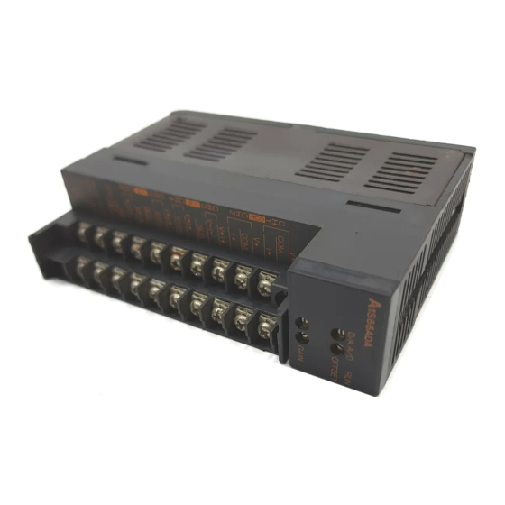
Page 30: Part Identification And Settings
4 PROCEDURES AND SETTINGS BEFORE OPERATION MELSEC-A 4.4 Part Identification and Settings The following describes the part names and settings of the A1S66ADA : A1S66ADA OFFSET 0-10V 0-5V 1-5V 10-10V GAIN V+ I+ V– I– V+ I+ V– I– V+ I+ V–... - Page 31 4 PROCEDURES AND SETTINGS BEFORE OPERATION MELSEC-A Name Description RUN LED Indicates the operating conditions of the A1S66ADA On : Power is ON Off : Power is OFF D/A conversion offset control knob Used when making a fine adjustment of the D/A conversion offset.
- Page 32 4 PROCEDURES AND SETTINGS BEFORE OPERATION MELSEC-A Name Description Analog ground terminal The ground terminal of the analog signal (Refer to Section 4.4 on the wiring method.) Frame ground terminal The ground terminal of the shielded cable (Refer to Section 4.4 on the wiring method.) Power supply input terminal Connect 24 V DC at the input terminal of the power supply.
-
Page 33: Wiring
(1) Use separate cables for the AC and the analog input to the A1S66ADA, in order not to be affected by the AC side surge or conductivity. -
Page 34: Wiring Between The A1S66Ada And The External Devices
4 PROCEDURES AND SETTINGS BEFORE OPERATION MELSEC-A 4.5.2 Wiring between the A1S66ADA and the external devices The following shows the wiring method for the A1S66ADA. (1) CH1 and CH2 (a) For voltage output Motor drive module, etc. CH1 or CH2... - Page 35 6 Due to noise in the environment, AG terminal may attain better accuracy when grounded. POINT • The FG terminal of A1S66ADA and the FG terminal of the power supply module are not connected. • In an unused channel, if terminals remain open, an erratic digital value may be output.
-
Page 36: Fine Adjustment Of The Offset /Gain Values
4.6.1 Fine adjustment methods of the offset/gain values The following flow chart describes the fine adjustment procedure of the offset/gain value of A1s66ADA. This setting is for when the module is installed in the slot No. 0, the D/A conversion to CH1 and A/D conversion to CH3. - Page 37 POINT Disconnect the power supply for the PLC CPU or the external power supply for A1S66ADA at all phases when setting the output range and making voltage/current selection. 4 - 11...
-
Page 38: Maintenance And Inspection
4 PROCEDURES AND SETTINGS BEFORE OPERATION MELSEC-A 4.7 Maintenance and Inspection The A1S66ADA has no particular inspection items, but in order to maintain the system in the best condition, perform inspection according to the categories listed in the PLC CPU Users' Manual. -
Page 39: Programming
5 PROGRAMMING The program creation procedures, basic read and write programs, and program examples for A1S66ADA are explained. When utilizing the program example introduced in this chapter for an actual system, fully verify that there are no problems in controllability in the target system. -
Page 40: Basic Read And Write Programs
X, Y where data is to be stored Example When assigning the A1S66ADA to I/O X40 to X7F and Y40 to Y7F, then writing the binary data stored in D10 to I/O signals Y40 to Y4B MOV instruction execution condition K3Y40 (2) Read from A1S66ADA·····················MOV, MOVP instruction... -
Page 41: Program Example
5 PROGRAMMING MELSEC-A 5.3 Program Example This program example converts the value set by the BCD digital switch into an analog value (voltage/current) and reads the digital values that have undergone A/D conversion at channels 3 through 6. When applying any of the program examples introduced in this chapter to the actual system, verify the applicability and confirm that no problems will occur in the system control. - Page 42 5 PROGRAMMING MELSEC-A Offset/gain setting X0040 Offset conversion setting D/A conversion offset value offset command 0 is input to Y00 to Y0B. setting Y0000 CH. 1 conversion digital offset value setting setting CH. 1 D/A conversion output Y000F enable flag is turned ON. CH.
-
Page 43: Troubleshooting
Measure the digital output value by disconnecting the Check the grounding method and wiring, as it may be cable for the analog input of the A1S66ADA then influenced by the noise from the external wiring, if the applying the test voltage (stabilized power supply or digital output values are normal at the individual batteries) to the terminal of the main module. - Page 44 6 TROUBLESHOOTING MELSEC-A MEMO 6 - 2 6 - 2...
-
Page 45: Appendix
APPENDIX MELSEC-A APPENDIX Appendix1 Comparison with the Conventional Analog I/O Module (A1S63ADA) Comparison of specifications for A1S66ADA with those for the conventional analog I/O module, A1S63ADA, is shown below. Specification Item A1S66ADA A1S63ADA Digital input Analog output Digital input Analog output... - Page 46 APPENDIX MELSEC-A Specification Item A1S66ADA A1S63ADA Simple loop control Not available Available Analog value read/write I/O signal method Buffer memory method method Within ±1 % (accuracy relative to the maximum value) Overall accuracy Between I/O terminal and PLC power supply··········Photocoupler insulation Insulation method Between channels····················································No insulation...
-
Page 47: Appendix 2 External Dimensions
APPENDIX MELSEC-A Appendix 2 External Dimensions A1S66ADA OFFSET GAIN V+ I+ V– I– V+ I+ V– I– V+ I+ V– I– V+ I+ V– I– (FG) INPUT 24VDC D/A A/D 0~±10 V 0~20 mA A1S66ADA 34.5 93.6 (3.69) (1.36) Unit: mm (in.) -
Page 48: Appendix 3 Precautions For Reading A Digital Output Value (For Hardware Version "C" Or Earlier)
If a digital output value is read from the PLC CPU during A/D conversion processing of the A1S66ADA (For Hardware Version "C" or Earlier), data may be read to the lower order byte (Xn0 to Xn7) and higher order byte (Xn8 to XnB) at different timings. - Page 49 As the value used for judgment, set "(input variation per scan) + (digital value for error 40)" or more. (1) System configuration Install the A1S66ADA on "Slot 0" of the main base. (2) Devices used by the user 1) Digital output value read command signal..........M0 2) Digital output value read switching signal..........M1...
- Page 50 WARRANTY Please confirm the following product warranty details before using this product. 1. Gratis Warranty Term and Gratis Warranty Range If any faults or defects (hereinafter "Failure") found to be the responsibility of Mitsubishi occurs during use of the product within the gratis warranty term, the product shall be repaired at no cost via the sales representative or Mitsubishi Service Company.
- Page 52 Analog Input/Output Module Type A1S66ADA User s Manual A1S66ADA-U-E MODEL MODEL 13JL41 CODE IB(NA)-66819-I(0707)MEE HEAD OFFICE : TOKYO BUILDING, 2-7-3 MARUNOUCHI, CHIYODA-KU, TOKYO 100-8310, JAPAN NAGOYA WORKS : 1-14 , YADA-MINAMI 5-CHOME , HIGASHI-KU, NAGOYA , JAPAN When exported from Japan, this manual does not require application to the Ministry of Economy, Trade and Industry for service transaction permission.