Sharp SL-5500 Service Manual
Personal mobile tool
Hide thumbs
Also See for SL-5500:
- Operation manual (148 pages) ,
- Software manual (92 pages) ,
- Startup manual (84 pages)
Quick Links
q
CHAPTER 1. SPECIFICATIONS . . . . . . . . . . . . . . . . . . . . . . . . . . . . 1
CHAPTER 2. HARDWARE DESCRIPTION . . . . . . . . . . . . . . . . . . . . 4
CHAPTER 3. DISASSEMBLY AND ASSEMBLY . . . . . . . . . . . . . . . 31
CHAPTER 4. NOTES FOR SERVICING . . . . . . . . . . . . . . . . . . . . . 47
CHAPTER 5. DIAGNOSTICS AND CHECK ITEMS . . . . . . . . . . . . . 50
CHAPTER 6. TROUBLE SHOOTING. . . . . . . . . . . . . . . . . . . . . . . . 60
CHAPTER 7. CIRCUIT DIAGRAM & PARTS LAYOUT . . . . . . . . . . 63
Parts marked with "!" are important for maintaining the safety of the set. be sure to replace these parts with specified
ones for maintaining the safety and performance of the set.
SERVICE MANUAL
Personal Mobile Tool
MODEL
CONTENTS
SHARP CORPORATION
CODE : 00ZSL5500SM/E
SL-5500
This document has been published to be used
for after sales service only.
The contents are subject to change without
once.

Related Manuals for Sharp SL-5500


Summary of Contents for Sharp SL-5500
-
Page 1: Table Of Contents
SERVICE MANUAL CODE : 00ZSL5500SM/E Personal Mobile Tool SL-5500 MODEL CONTENTS CHAPTER 1. SPECIFICATIONS ......1 CHAPTER 2. -
Page 2: Chapter 1. Specifications
Palmtop Environment (both by Trolltech) for its Linux application platform, and further implements PersonalJava environment (Jeode by Insignia Solutions) to execute PersonalJava applications. By implementing both Linux and Java, which are open and standard platform, anyone may develop application software for the SL-5500 by using existing and easily available tools. - Page 3 Memory backup battery (Built-in): 3.0V DC Battery life When the power of the SL-5500 is turned on at a temperature of under 25°C (75°F), with no peripheral device (including the CF memory card) connected, after the rechargeable battery (EA-BL06) is fully charged.
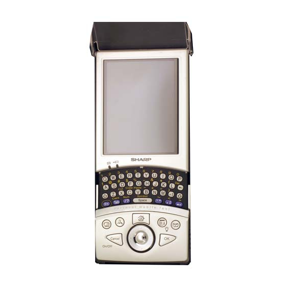
- Page 4 Cancel key (On/Off key) OK key Select key Cursor key Keyboard Display Protection cover Slide Cover SHARP I/O PORT AC Adapter Jack Back Eyelets for the Handstrap Battery Compartment Lid FULL RESET button Battery Replacement Switch Rear S tylus CF Card Slot...
-
Page 5: Chapter 2. Hardware Description
PC-UM10M CHAPTER 2. HARDWARE DESCRIPTION 1-1. BLOCK DIAGRAM SL-5500 HARDWARE DESCRIPTION – 4 –... - Page 6 (from LOCOMO) /MIC_ON Docking Station MIC_INPUT Serial ch3(UART) WAKEUP(to CPU GP24) USB FUNCTION RXD3 TXD3 SERIAL(CMOS-level) Serial ch0(USB) UDC- UDC+ VCC3 (from TC35143)Analog OUT Sounder PWR+ / - Adapter (from TC35143)Sounder bias D+_1.5k_on(from SCOOP PA19) SL-5500 HARDWARE DESCRIPTION – 5 –...
- Page 7 – Supports two PCMCIA sockets VDDX Supply nTRST VSS/VSSX * Power dissipation, particularly in idle mode, is strongly dependent on the details of the system design. *Other brands and names are the property of their respective owners. SL-5500 HARDWARE DESCRIPTION – 6 –...
- Page 8 PCMCIA output enable. This signal is an output and is used to perform reads from memory and attribute space. nPWE PCMCIA write enable. This signal is an output and is used to perform writes to memory and attribute space. SL-5500 HARDWARE DESCRIPTION – 7 –...
- Page 9 When nRESET is driven high, the processor will restart from address 0. nRESET must remain low until the power supply is stable and the internal 3.686-MHz oscillator has come up to speed. While nRESET is low, the processor will perform idle cycles. SL-5500 HARDWARE DESCRIPTION – 8 –...
- Page 10 Data Bus • Programmable speaker output level attenuator (8 stages in steps of 3dB) Flash Peripheral • Programmable sampling frequency (4 stages in steps of 8 kHz, about 11.03 kHz, 16 kHz, about 22.05 kHz) SL-5500 HARDWARE DESCRIPTION – 9 –...
- Page 11 Negative polarity input terminal for telephone line CODEC. Open when not in use. VBO1P Positive polarity output terminal 1 for sound CODEC. It is used for the handset speaker. VBO1N Negative polarity output terminal 1 for sound CODEC. It is used for the handset speaker. SL-5500 HARDWARE DESCRIPTION – 10 –...
- Page 12 • DEF means reset state. H/L stand for output levels. Hz means high impedance and IN means input state (high impedance). • Group categories are as follows : HOST-Host interface, TSC-Touch screen interface, TEL-Telecom CODE, VB-Voice band CODEC, ETC-The other, POW-power supply. SL-5500 HARDWARE DESCRIPTION – 11 –...
- Page 13 • Settable partition configuration • Page buffer program • Data protection function for each block and full-block lock function at power-on. • 8-word OTP (One Time Program) block • Low power consumption • Parameter block configuration SL-5500 HARDWARE DESCRIPTION – 12 –...
- Page 14 (High Z). Data is erased or The LOCOMO-QFP15-128pin G/A (SLA5075H) is a gate array devel- latched internally while a program is run- ning. oped for the SL-5500. Input Chip enable: This pin activates device con- The outlines of built-in functions are described below.
- Page 15 Internal status register Xout 18m bit 1(CLK9M) output pin dividing CLK9M output pin circuit Xin 18m input pin SPI block XON signal CLK32K block XON signal Initialize CPU bus CLK9MEN battfault input pin Register settings SL-5500 HARDWARE DESCRIPTION – 14 –...
- Page 16 DAC power supply ON 3.3~ Power supply 5.0V ON/OFF Input pin COMADJ I/O pin Backlight voltage SDAOEB output pin light input pin control General-purpose Initialize battfault 8-bit DAC SCLOEB (Mitsubishi input pin M62332FP) Register settings SL-5500 HARDWARE DESCRIPTION – 15 –...
- Page 17 Nos. 98 and 99 pins (xin22m, xout22m):22.5792MHz (ceramic oscillator) Correct matching is required. Note 2: Nos. 11-27 pins (data [15:0] data bus): Bus cycle 30MHz Nos. 72-82 pins (adr [7:2], [25:23] address bus): Bus cycle 30MHz SL-5500 HARDWARE DESCRIPTION – 16 –...
- Page 18 Oscillation circuit 2 (OSC4C) XOUT24M 48 KHz system base clock output Oscillation circuit 2 (22.5792 MHz) (OSC4C) CLK64FS OB2T Audio 64 fs output (SCLK x2) CPU (GPI0) MCLK OB2T Audio MCLK clock output Audio DAC Subtotal SL-5500 HARDWARE DESCRIPTION – 17 –...
- Page 19 : AND type gated I/O buffer (IOL=2mA, with test function) BA2T : AND type gated I/O buffer (IOL=6mA, with test function) : TRANSPARENT input buffer (for clock oscillation) : TRANSPARENT output buffer (for clock oscillation) ITST1 : Test mode input buffer (with pull-down) SL-5500 HARDWARE DESCRIPTION – 18 –...
- Page 20 Blue data signal input pin (LSB) Gate driver clock signal output pin Blue data signal input pin Gate driver start signal output pin Blue data signal input pin Power supply input pin – Blue data signal input pin SL-5500 HARDWARE DESCRIPTION – 19 –...
- Page 21 Horizontal timing I-b (When ENAB signal is used.) (Te+308)DCLK-440DCLK 12DCLK 0.4Tc~0.6Tc 50us~120us 50us~120us DCLK 50us Above R0~R5 D319 D320 G0~G5 B0~B5 14DCLK-71DCLK 50us~120us ENAB 320DCLK OR0~OR5 OG0~OG5 OD1 OD2 OD3 OD319 OD320 OB0~OB5 1DCLK 1DCLK 14DCLK 1DCLK 9DCLK 289DCK 3DCLK SL-5500 HARDWARE DESCRIPTION – 20 –...
- Page 22 #REG nPCE(1:2) #CD(1:2) nPOE nPWE nPIOW #IOR nPIOR #IOW nPWAIT #WAIT WP/#IOIS16 nPIOIS16 #CS4 #CCD1 #CCD2 BVD1/STSCH Inside REG BVD2/#SPKR #CRESET #RESET INTC #CVS1 #CVS2 INTPCCARD #CVCCDOWN #CVCC3EN #CVCC5EN #CVPP3EN #CVPP5EN IC401 VACT SL-5500 HARDWARE DESCRIPTION – 21 –...
- Page 23 PA20 value). The pull-down resistance value is 40k-240kΩ (TYP100kΩ) SA1110 (CPU) Scoop (CF card mode.) Panel controller 2. These pins are basically used for address bus input, and thus input is not Schmitt received. SL-5500 HARDWARE DESCRIPTION – 22 –...
- Page 24 Port DATA Filter Over- Enhanced sampling Multi-level Digital VCOM Delta- Filler Slgma with Serial Modulator Output Amp Function Control and Low-pass Controller Port Filter VOUTR System Clock System Zero Detect Power Supply Clock Manager SL-5500 HARDWARE DESCRIPTION – 23 –...
- Page 25 MGM667 (4) PINNING SYMBOL DESCRIPTION conversion mode selection input ILIM current limit resistor connection UPOUT/DNIN upconversion output voltage downconver- sion input voltage inductor connection SYNC synchronization clock input ground feedback input SHDWN shut-down input SL-5500 HARDWARE DESCRIPTION – 24 –...
- Page 26 ILIM Inductor current limit programming pin. Tie pin to VIN for 0.95A peak inductor current limit. Tie pin to ground for 0.5A peak inductor current limit. TTL input threshold. SL-5500 HARDWARE DESCRIPTION – 25 –...
- Page 27 PC-UM10M 2-12. HOW TO USE EACH LSI PIN ON THE SL-5500 SL-5500 Direction Level at OFF SA1110 GPIO0 Reserve ON_KEY from KEY Default: Both edges enable 1 Reserve AC_IN AC at “H” Default: Both edges enable 2 LCD_8 LCD_8 3 LCD_9...
- Page 28 ON at HI LCD_MOD DAC_ON ON at HI F/L_VR Large current (bright) at PCM_SDATA PCM_SCK PCM_SLOAD nSD_DETECT Detected at LOW SD_WP WP state at HI SD_VCC_ON ON at HI ADSTART TFTRESET CLK9M DACSCK LRCLK SL-5500 HARDWARE DESCRIPTION – 27 –...
- Page 29 L/B VOLTAGE CHNG USB D+ signal pull-up resistor control (Enabled at “H”) PA20 LCD TIMING ADJUST- INPUT MENT F/F CLK PA21 LCD TIMING ADJUST- INPUT MENT F/F DATA PA22 LCD TIMING ADJUST- MENT F/F Q SL-5500 HARDWARE DESCRIPTION – 28 –...
- Page 30 PC-UM10M 3. ABOUT THE SYSTEM OF SL-5500 3-1. SYSTEM OUTLINE 3-2. AUDIO CONTROL Item SL-5500 CLK64fs CLK64fs MCLK SCLK SA1110 Rev.B4 SCLK BCKIN JACK SFRM SFRM nCS0 3 16MB LRCIN LRCLK ROMP capacity SDOUT (x32 bus fixed) nCS1 3 Not Use...
- Page 31 3.3V or 5V SW3 = ON Regurater FET SW (TK11133CS) SW4 = OFF During set OFF (Main battery voltage >3.3V) SD CARD CF CARD Plus 5V DC/DC=ON (3.8V output) SW3 = OFF SW4 = ON SL-5500 HARDWARE DESCRIPTION – 30 –...
-
Page 32: Chapter 3. Disassembly And Assembly
Cover more than 135 degrees the both sides one by one. will cause the cover to come 3 If the card is inserted forcibly in the wrong direction, it may be OFF. broken. SL-5500 DISASSEMBLY AND ASSEMBLY – 31 –... - Page 33 (1) Disengage the upper and the lower cabinets on the right side upward to remove it from the Lower Cabinet. (SD slot side) when viewed from the back of the SL-5500. Since there is no lock pawl in this section, they can be disen- Stereo Headphone Jack gaged with a slight force.
- Page 34 PC-UM10M [NOTE FOR ASSEMBLY] Note for removing the Lower Cabinet of the SL-5500 When removing the Lower Cabinet, do not shake the Lower Cabinet 1. Battery Take-Out Ribbon attachment right and left. If it should be shaken with an excessive force, the boss on...
- Page 35 The Cool CRT lead wire must not extend from the Stylus Holder. Check that the PWB is not on the LCD holder rib B when assembling the lower cabinet. (If it is on, an assembly error will occur.) SL-5500 DISASSEMBLY AND ASSEMBLY – 34 –...
- Page 36 (upper and lower sides). Apply grease to this area of the groove (upper and lower sides). Apply a small amount of grease to the corners. Apply a small amount grease corners. (a) - (a) cross section SL-5500 DISASSEMBLY AND ASSEMBLY – 35 –...
- Page 37 • When tightening the screws, do not apply an excessive force. When tightening the screw , hold When tightening the this section to screw , hold this prevent the Rib section to prevent PWB from rotating. the Rib PWB from rotating. Boss Cap SL-5500 DISASSEMBLY AND ASSEMBLY – 36 –...
- Page 38 (1) When processing the lead wire of the Cool CRT, be careful not to damage the coating cover. • Never use a sharp cutter for processing of the lead wire. • Never use the Cool CRT with damaged or broken coating cover of lead wire.
- Page 39 (12)Check that the PWB Unit 7 is securely fixed by the LCD Holder • Never use a sharp cutter for processing of the lead wire. 6 Pawl. (13)The tablet pin 1 cannot be connected after attaching the •...
- Page 40 Check that the Slide Cover is fixed to the cabinet rib at two posi- Slide Cover Panel Fixing Tape tions. Slide Cover Fixture 3. Screw A (x 4) tightening Be careful not to apply an excessive force. Screw A Screw A SL-5500 DISASSEMBLY AND ASSEMBLY – 39 –...
- Page 41 (2) When taking/reversing the Key Rubber B, be careful not to drop the Key Top. (3) Be careful to prevent the Key Rubber/Key Top from covering the cabinet ribs and key holes. Key rubber B SL-5500 DISASSEMBLY AND ASSEMBLY – 40 –...
- Page 42 (2) Separate the Slide Cover Panel Fixing Tape from the Mount Sheet. (3) Attach the Slide Cover Panel Fixing Tape to the Slide Cover Panel. Note: Attach the tape so that it does not cover the rib. SL-5500 DISASSEMBLY AND ASSEMBLY – 41 –...
- Page 43 –0.0mm (Must not extend over the step.) Y direction: +0.0mm (Must not extend over the step.) –0.1mm C surface (Attachment direction mark) +0.1 Attachment reference (Y direction) -0.1 Tablet upper mask a - a cross section SL-5500 DISASSEMBLY AND ASSEMBLY – 42 –...
- Page 44 Contact Spring Unit Attachment reference CF Tape 2. Applying grease to the I/O Holder. I/O Holder I/O Cover I/O Holder Grease application area Apply grease also to the same area on the other side. SL-5500 DISASSEMBLY AND ASSEMBLY – 43 –...
- Page 45 (PWB outward form line) -0.2 [CF Tape attachment] Attachment reference Attachment reference pattern pattern CF Card Connector Frame Do not hang on this metal Attachment reference -0.5 +0.5 Attachment reference CF Tape Folding attachment SL-5500 DISASSEMBLY AND ASSEMBLY – 44 –...
- Page 46 Be sure to make close contact of the at 3 positions Contact Spring Unit on the back Soldering at 4 positions Stereo Headphone Jack. of pins Coverage soldering to Coverage soldering to the Hold Down section the Hold Down section SL-5500 DISASSEMBLY AND ASSEMBLY – 45 –...
- Page 47 Y direction (External shape of sub PWB) 0.8mm Back Up Battery Cushion Solder Never put a circuit board on another or never put it on a metal surface. SL-5500 DISASSEMBLY AND ASSEMBLY – 46 –...
-
Page 48: Chapter 4. Notes For Servicing
(2) HARDWARE RESET Note: • If the Welcome screen doesn’t appear, try FULL RESET again. If the SL-5500 still fails to function after the software reset is done Also check the Battery Replacement Switch is set to “NORMAL shown above, you will have to do hardware reset. - Page 49 FULL RESET button down for a few sec- onds. AC Power Cord 3. Connect the PC’s parallel port and the SL-5500 with the JTAG cable. 4. Start the command prompt on the PC. 2. Plug the AC Adapter connector into the SL-5500 which contains the Move to the folder where the above program was unpacked, using battery as shown to the below.
- Page 50 Note: If you cannot exit the program successfully, remove the Main ROM in the device will start. Battery and AC Adapter from the SL-5500 and repeat the above Caution: Please don’t abort or remove the AC Adapter until the LED procedure.
-
Page 51: Chapter 5. Diagnostics And Check Items
When the Normal Diag Mode (Diag Menu (3/3) No. 10) is executed, if “Full reset” is made, the diag is booted. To boot the OS, execute Clear Diag Flag (Diag Menu (3/3) No.4). SL-5500 DIAGNOSTICS AND CHECK ITEMS – 50 –... - Page 52 Green Connect the AC adapter, supply power to the DIAG MENU (1/3) DIAG is booted. SL-5500, and press the FULL RESET button. Touch No. 5 LCD + LED. White background White background is displayed. F/L turns on. Press [OK] key.
- Page 53 PC-UM10M CURRENT CONSUMPTION CHECK Operating procedure Display Check item Check that the SL-5500 battery replacement switch is locked. As shown in Fig-1, supply power to the SL- DIAG MENU (1/3) 5500. V1 = 3.8V Boot the diag mode (SW1~SW3 = ON)
- Page 54 [Fn] [Tab] [/?] [Space] [‘ “] [. :] [ENTER] Press [OK] key to return to the menu. DIAG MENU (1/3) Press [on/off] key to turn off the power. After the display is turned off completely, disconnect the AC adapter. SL-5500 DIAGNOSTICS AND CHECK ITEMS – 53 –...
- Page 55 Display Check item Connect the AC adapter to supply power to the SL-5500. Press FULL RESET button to boot the DIAG mode. If the DIAG is not booted by pressing FULL RESET button, press and hold [P] + [D] and press FULL RESET button simultaneously.
- Page 56 Display Check item Connect the AC adapter to supply power to the DIAG MENU (1/3) SL-5500, and press FULL RESET button to boot the DIAG menu. Press Front Light key to turn on the light. DIAG MENU (1/3) Select No. 4 Touch Panel.
- Page 57 Use the cursor key to open "DIAG MENU (3/3)" . Tap "No.1 IrDA Checker." Open "DIAG MENU (1/3)" . Face the IrDA port of the target SL-5500 toward that of the checker SL-5500. Tap "No.6 IrDA." === IrDA check Slave === Push [On] button to menu 1If "OK"...
- Page 58 Copy the data in the machine to the SD card. If copying is performed normally, it is OK. For operating procedures, refer to the Operation Manual. 4) USB PORT TEST (SOME OF SHARP I/O PORTS (16PIN CONNECTOR)) Test by OS...
- Page 59 PC-UM10M 5) SERIAL PORT TEST (SOME OF SHARP I/O PORTS (16PIN CONNECTORS)) 1. Control line test Test by Diag Test jig: Use the following circuit. (Prepare it on each service spot.) Open "DIAG MENU (2/3) ". Connect the following test circuit.
- Page 60 Data 15-8, REG#, WE#, RD# Data7-0, CE1# IOWR#, IORD#, WAIT# AddressBus A10-A0, CE1#, CE2#, OE# VCC, BVD1, BVD2, WP, RDY VS1, VS2 At last, if the display indicates as below, it is OK. ----- Status messages----- SL-5500 DIAGNOSTICS AND CHECK ITEMS – 59 –...
-
Page 61: Chapter 6. Trouble Shooting
If the user data should be recovered, back up the user If the figure is 1000 or greater, it might be considered that no data before executing the diag operations. battery is inserted. Replace the battery with new one. LED (A) SL-5500 TROUBLE SHOOTING – 60 –... - Page 62 Some change: Check the VCOM signal of the LCD unit from IC301 1 pin. diag menu? No display: Check soldering of IC501/IC901. 2) Does X903 oscillate? ( X903 = 18.432 MHz) 3) Is FPC of the tablet disconnected? Is it properly connected to the connector? SL-5500 TROUBLE SHOOTING – 61 –...
- Page 63 When the "WAIT" signal of the card is at no operation is "LOW", no operation is performed. (Wait performed. is applied to the operation.) Check IC401 and BR402. (Check that soldering is properly made and that the resistors are not broken.) SL-5500 TROUBLE SHOOTING – 62 –...
-
Page 64: Chapter 7. Circuit Diagram & Parts Layout
PC-UM10M SL-5500 CIRCUIT DIAGRAM & PARTS LAYOUT – 63 –... - Page 65 PC-UM10M SL-5500 CIRCUIT DIAGRAM & PARTS LAYOUT – 64 –...
- Page 66 PC-UM10M SL-5500 CIRCUIT DIAGRAM & PARTS LAYOUT – 65 –...
- Page 67 PC-UM10M SL-5500 CIRCUIT DIAGRAM & PARTS LAYOUT – 66 –...
- Page 68 PC-UM10M SL-5500 CIRCUIT DIAGRAM & PARTS LAYOUT – 67 –...
- Page 69 PC-UM10M SL-5500 CIRCUIT DIAGRAM & PARTS LAYOUT – 68 –...
- Page 70 PC-UM10M SL-5500 CIRCUIT DIAGRAM & PARTS LAYOUT – 69 –...
- Page 71 PC-UM10M SL-5500 CIRCUIT DIAGRAM & PARTS LAYOUT – 70 –...
- Page 72 PC-UM10M SL-5500 CIRCUIT DIAGRAM & PARTS LAYOUT – 71 –...
- Page 73 PC-UM10M SL-5500 CIRCUIT DIAGRAM & PARTS LAYOUT – 72 –...
- Page 74 PC-UM10M SL-5500 CIRCUIT DIAGRAM & PARTS LAYOUT – 73 –...
- Page 75 PC-UM10M SL-5500 CIRCUIT DIAGRAM & PARTS LAYOUT – 74 –...
- Page 76 PC-UM10M SL-5500 CIRCUIT DIAGRAM & PARTS LAYOUT – 75 –...
- Page 77 PC-UM10M SL-5500 CIRCUIT DIAGRAM & PARTS LAYOUT – 76 –...
-
Page 78: Parts Guide
Parts guide 1 Exteriors SLIDE COVER UNIT MAIN PWB UNIT SUB PWB UNIT UPPER CABINET UNIT LOWER CABINET UNIT LCD+PWB UNIT DOCKING STATION CCP00163 – 1 –... - Page 79 1 Exteriors PRICE PART PARTS CODE DESCRIPTION RANK MARK RANK 1 L X - B Z 1 0 2 6 Y C Z Z Screw C (M14) 2 P G U M M 1 0 3 1 Y C Z 1 Key rubber A 3 D U N T G 2 1 9 7 Y C S 2 Slide cover unit...
- Page 80 2 Packing material & Accessories PRICE PART PARTS CODE DESCRIPTION RANK MARK RANK Q A C C D 1 3 1 1 Q C Z Z AC cord (10A-BUSH2M) [SEC/SECL,OTHER] Q A C C B 3 3 2 1 Q C Z Z AC cord (13A-BUSH2M) [SUK,SRH] Q A C C E 3 3 2 1 Q C Z Z...
- Page 81 3 Main PWB unit PRICE PART PARTS CODE DESCRIPTION RANK MARK RANK 42 R M P T R 2 2 2 3 Q C J J Block resistor (22KΩ×2(1005)) [BR704] 43 R M P T R 2 4 7 3 Q C J J Block resistor (47KΩ×2) [BR806,BR402] R M P T R 2 4 7 4 Q C J J...
- Page 82 3 Main PWB unit PRICE PART PARTS CODE DESCRIPTION RANK MARK RANK 106 V H I T K 1 1 1 3 3 C - 1 IC (TK11133CS) [IC502,IC308,IC605] 107 V H P G P 2 W 0 1 1 0 - 1 IR unit (GP2W0110YP) [IR701] 108 V H P L T 1 F 6 7 A F - 1...
- Page 83 3 Main PWB unit PRICE PART PARTS CODE DESCRIPTION RANK MARK RANK 205 Q J A K C 1 0 1 5 Y C Z Z Stereo headphone jack [CN603] 206 Q T A N B 1 0 5 1 Y C Z Z Contact spring unit [CN701,CN702] 207 V H D D S P 1 0 G + + - 1...
- Page 84 © COPYRIGHT 2002 BY SHARP CORPORATION All rights reserved. Printed in Japan. No part of this publication may be reproduced, stored in a retrieval system, or transmitted. In any form or by any means, electronic, mechanical, photocopying, recording, or otherwise, without prior written permission of the publisher.