Table of Contents

Related Manuals for Panasonic SA-DK3


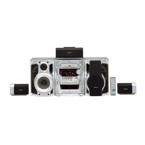
Summary of Contents for Panasonic SA-DK3
- Page 1 ORDER No.MD0005092C1 DVD Stereo System SA-DK3 Colour (S) ....Silver Type Areas (PP) ....U.S.A. and Canada TAPE SECTION : AR2 MECHANISM SERIES CD SECTION : DPT-4AT-AD TRAVERSE DECK SERIES SYSTEM : SC-DK3 SPECIFICATIONS Specifications...
-
Page 2: Amplifier Section
AMPLIFIER SECTION Front speaker power output RMS power output THD 1.0%, both channels driven 55Hz - 120Hz 100W per channel (6 120Hz - 4kHz 30W per channel (6 4kHz - 15kHz 30W per channel (6 160W per channel Total tri-amp power Power output in Dolby Pro Logic RMS power output THD 1.0%, both channels driven... -
Page 3: Disc Section
Fast forward and rewind time Approx. 120 seconds with C -60 cassette tape DISC SECTION Disc DVD-Video 8cm/12cm single-sided, single-layer / 8cm/12cm single- sided, double-layer / 8cm/12cm double-sided, double-layer / (One layer per side) Video CD/CD 8cm/12cm Video Signel system NTSC Output level Composite video 1Vp-p (75... -
Page 4: Safety Precaution
Licensing Corporation. DOLBY, the double-D symbol and “PRO LOGIC” are trademarks of Dolby Laboratories Licensing Corporation. SYSTEM SC-DK3 : / Main unit : SA-DK3 / Front speakers : SB-AK78 / Surround speakers : SB-PS70 / Center Speakers : SB-PC70 1. Safety Precaution (This “Safety Precaution”... -
Page 5: Before Repair And Adjustment
screwheads, antenna, control shafts, handle brackets, etc. / Equipment with antenna terminals should read between 2.7M and3.9M to all exposed parts*. ( Fig.1 ) / Equipment without antenna terminals should read approximately infinity to all exposed parts. ( Fig.2 ) / *Note: Some exposed parts may be isolated from the chassis by design. -
Page 6: Handling Precautions For Traverse Deck
outlines below: 1. Turn off the power. 2. Determine the cause of the problem and correct it. 3. Turn on the power once again after one minute. Note: When the protection circuitry functions, the unit will not operate unless the power is first turned off and then on again. 4. - Page 7 5.2. Grounding for electrostatic breakdown prevention 1. Human body grounding / Use the anti-atatic wrist strap to discharge the static electricity from your body. 2. Work table grounding / Put a conductive material (sheet) or steel sheet on the area where the optical pickup is placed, and ground the sheet.
-
Page 8: Precaution Of Laser Diode
CAUTION: THIS PRODUCT UNTILIZES A LASER. USE OF CONTROLS OR ADJUSTMENTS OR PERFORMANCE OF PROCEDURES OTHER THAN THOSE SPECIFIED HEREIN MAY RESULT IN HAZARDOUS RADIATION EXPOSURE. 6. Precaution of Laser Diode CAUTION: This product utilizes a laser diode with the unit turned “ON”, invisible laser radiation is emitted from the pick up lens. - Page 9 8. Location of Controls for Remote Control Transmitter...
-
Page 10: Operation Checks And Component Replacement Procedures
9. Operation Checks and Component Replacement Procedures - This section describes procedures for checking the operation of the major printed circuit boards and replacing the main components. - For reassembly after operation checks or replacement, reverse the respective procedures. Special reassembly procedures are described only when required. - Page 11 9.1. Checking for the main P.C.B. and DVD module (1) P.C.B.
- Page 12 - Check the main P.C.B. and DVD module (1) P.C.B. (A side) as shown below.
- Page 13 - Check the DVD module (1) P.C.B. (B side) as shown below. 9.2. Disassembly for the DVD changer unit (The DVD changer unit can be removed until the tray base / ornament would removed.) 9.2.1. Disassembly for the disc tray ornament - Follow the (Step 1) - (Step 3) of item 9.1.
- Page 15 9.2.2. Disassembly for the DVD changer unit - Follow the (Step 1) - (Step 3) of item 9.1. - Follow the disassembly instruction for the disc tray / ornament of item 9.2.1.
- Page 17 9.3. Checking for the unit operational condition (Place the unit horizontally when loading the DVD changer unit.) 9.3.1. Initial setting of DVD/CD - Follow the (Step 1) - (Step 3) of item 9.1. - Follow the disassembly instruction for the disc tray / ornament of item 9.2.1.
- Page 18 9.3.2. Checking for the DVD module (2) P.C.B. - The initial setting of DVD/CD unit must be completed. / (Refer to the initial setting of DVD/CD unit in item 9.3.1.)
- Page 19 - Check the DVD module (2) P.C.B. as shown below.
- Page 20 9.3.3. Checking for the FL P.C.B., cassette mechanism control P.C.B., regulator P.C.B. and power supply P.C.B. - The initial setting of DVD/CD unit must be completed. / (Refer to the initial setting of DVD/CD unit in item 9.3.1.) - Check the FL P.C.B., cassette mechanism control P.C.B. and regulator P.C.B.
- Page 22 - Check the power supply P.C.B. as shown below. 9.4. Replacement for the traverse deck ass’y - Follow the (Step 1) - (Step 3) of item 9.1. - Follow the disassembly instruction for the disc tray / ornament of item 9.2.1. - Follow the disassembly instruction for the DVD changer / unit of item 9.2.2.
-
Page 26: Replacement For The Disc Tray
9.5. Replacement for the disc tray - Follow the (Step 1) - (Step 3) of item 9.1. - Follow the disassembly instruction for the disc tray / ornament of item 9.2.1. - Follow the disassembly instruction for the DVD changer / unit of item 9.2.2. -
Page 29: Disassembly And Reassembly For Mechanism Base Drive Unit
9.6. Disassembly and reassembly for mechanism base drive unit - Follow the (Step 1) - (Step 3) of item 9.1. - Follow the disassembly instruction for the disc tray / ornament of item 9.2.1. - Follow the disassembly instruction for the DVD changer / unit of item 9.2.2. -
Page 42: Replacement For The Motor Ass'y
9.7. Replacement for the motor ass’y - Follow the (Step 1) - (Step 3) of item 9.1. - Follow the disassembly instruction for the disc tray / ornament of item 9.2.1. - Follow the disassembly instruction for the DVD changer / unit of item 9.2.2. - Page 43 9.8. Replacement for the traverse motor ass’y, optical pickup and spindle motor ass’y - Follow the (Step 1) - (Step 3) of item 9.1. - Follow the disassembly instruction for the disc tray / ornament of item 9.2.1. - Follow the disassembly instruction for the DVD changer / unit of item 9.2.2.
- Page 44 - Follow the (Step 1) - (Step 14) of item 9.4.
- Page 47 9.9. Replacement for the pinch roller ass’y and head block - Follow the (Step 1) - (Step 3) of item 9.1. - Follow the disassembly instruction for the disc tray / ornament of item 9.2.1. - Follow the disassembly instruction for the DVD changer / unit of item 9.2.2.
- Page 48 - Follow the (Step 1) - (Step 4) of item 9.3.3.
- Page 50 9.10. Replacement for the CD motor ass’y, capstan belt A, capstan belt B and winding belt - Follow the (Step 1) - (Step 3) of item 9.1. - Follow the disassembly instruction for the disc tray / ornament of item 9.2.1. - Follow the disassembly instruction for the DVD changer / unit of item 9.2.2.
- Page 53 9.11. Replacement for the component parts on the mechanism P.C.B. - Follow the (Step 1) - (Step 3) of item 9.1. - Follow the disassembly instruction for the disc tray / ornament of item 9.2.1. - Follow the disassembly instruction for the DVD changer / unit of item 9.2.2.
-
Page 54: Replacement For The Cassette Lid Ass'y
9.12. Replacement for the cassette lid ass’y - Follow the (Step 1) - (Step 3) of item 9.1. 9.13. Measure for tape trouble - Follow the (Step 1) - (Step 3) of item 9.1. - Page 55 10. Measurements and Adjustment 10.1. Cassette Deck Section 10.1.1. Measuring Instruments and Special Tools - Digital frequency counter - EVM-AC (AC Electronic voltmeter) - Test tape / QZZCFM : Head azimuth adjustment / QZZCWAT : Tape speed adjustment / QZZCRA : Normal reference blank tape / QZZCRX : CrO2 tape 10.1.2.
- Page 56 azimuth. (Shown in Fig.1 ). / Even if you wish to readjust the head azimuthwithout replacing the screws and springs, a fine adjustment cannot be done because of the screw-locking bond adhered to the azimuth screw and spring. - Please remove the screw-locking bond left on the head base when replacing the azimuth screw.
- Page 57 Fig.3 Fig.4 10.1.3. Tape Speed Adjustment (Deck 1/2) 1. Insert the test tape (QZZCWAT) to Deck 2 and playback (FWD side) the middle portion of it. 2. Adjust motor VR (Deck 2) for the output value shown below. / Adjustment target : 2940 - 3060Hz (NORMAL speed) 3.
- Page 58 the value of the output frequency of DECK2 FWD. Fig.5 Fig.6 10.1.4. Bias OSC Frequency Adjustment / (Deck 2) 1. Set the unit to “AUX” position. 2. Insert the Normal blank tape (QZZCRA) into DECK2 and set the unit to “REC” mode (use “ REC/STOP” key). 3.
- Page 59 value. 4. Insert the CrO2 tape (QZZCRX). 5. Repeat step 2 and 3. / Standard value (Normal) : 19±4mV / Standard value (CrO2) : 27 ±5mV Fig.8 10.1.6. Erase Voltage Check 1. Set the unit to “AUX” position. 2. Insert the Normal blank tape (QZZCRA) into DECK2 and set the unit to “REC”...
-
Page 60: Schematic Diagram Notes
11. Illustration of ICs, Transistors and Diodes 12. Schematic Diagram 12.1. Schematic Diagram Notes - This schematic diagram may be modified at any time with the development of new technology. Notes: : Tray position 1 detect switch in OFF position : Tray position 2 detect switch in OFF position : Tray open detect switch in OFF position... - Page 61 : Joystic up switch ( S619 : Joystic down switch ( S620 : CD manager switch (CD MANAGER) S621 : Disc1 direct play switch (CD1) S622 : Disc1 direct open/close switch ( S623 : Disc2 direct play switch (CD2) S624 : Disc2 direct open/close switch ( S625 : Disc3 direct play switch (CD3)
- Page 62 : Deck1 CrO2 tape detect switch (ATS/ S953 CrO2) : Deck2 mode detect switch (MODE) S971 : Deck2 half detect switch (HALF) S972 : Deck2 CrO2 tape detect switch (ATS/ S973 CrO2) : Deck2 reverse side record prevention tab S974 detect switch / (R.REC.INH) : Deck2 forward side record prevention tab S975...
-
Page 63: Printed Circuit Board Diagram
- Voltage and signal line / : Positive voltage line / Negative voltage line / : Audio/Front MID SP. drive signal line / : FM signal line / : FM OSC signal line / : AM signal line / : AM OSC signal line / Tape playback signal line / : Tape recording signal line / Sub woofer/frontlow SP. - Page 64 Function Terminal Name SPE IN Speana signal input 2 DECK2 Deck2 mechanism condition input 3 DECK1 Deck1 mechanism condition input KEY5- Operation switch signal input KEY1 9 JOG1B Volume control signal input 10 JOG1A Volume control signal input CT timer control 12 JOG2B Jog control signal input 13 JOG2A...
-
Page 65: Replacement Parts List
Function Terminal Name XC IN Oscillator connection / (Sub clock : 32.768MHz) 37 XC OUT Oscillator connection / (Sub clock : 32.768MHz) X IN Oscillator connection (Sub clock : 8.0MHz) 39 X OUT Oscillator connection (Sub clock : 8.0MHz) 41 MBP1 MPU beat proof output signal 42 MBP2 MPU beat proof output signal... -
Page 66
parts which have purposes of fire-retardant (resistors), hight- quality sound (capacitors), low-noise (resistors),etc. are used. / When replacing any of components, be sure to use only manufactures specified parts shown in the parts list. - The
mark in Remarks indicates source of supply. - The marking (RTL) indicates thet Retention Time is Limited for this item. - Page 67 Ref. No. Part No. Part Name & Description Pcs. Remarks RYQ0289-S JOY UNIT 1 [M] RMKX0036A BOTTOM CHASSIS 1 [M] RMKX0038A CD CHASSIS 1 [M] SHE187-4 SPACER (TRANS) 2 [M] RMC0399 REGULATOR CLUMPER 1 [M] RMN0578 REGULATOR PCB HOLDER 1 [M] REM0072-3 1 [M] RGR0297C-A1...
- Page 68 Ref. No. Part No. Part Name & Description Pcs. Remarks RMB0312 TRIGGER LEVER SPRING 2 [M] RMB0400 REEL SPRING 4 [M] RMB0403 HEAB PANEL SPRING 2 [M] RMB0404 BRAKE ROD SPRING 2 [M] RMB0406 FR LEVER SP 2 [M] RMB0408 THRUST SPRING 2 [M] RML0370...
- Page 69 Ref. No. Part No. Part Name & Description Pcs. Remarks RML0521 REAR LOCK LEVER 1 [M] RME0257 TRAY LOCK LEVER SPRI 1 [M] RML0520 TRAY LOCK 1 [M] RMM0202 SLIDE PLATE 2 1 [M] XTB3+10J SCREW 6 [M] RMR1302-W FIXED PLATE 1 [M] RMR1301-K CLAMPER...
-
Page 70: Integrated Circuits
Ref. No. Part No. Part Name & Description Pcs. Remarks VMC1487 SUB-SHAFT SPRING VMC1606 SPRING HOLDER 1 VMC1607 SPRING HOLDER 2 VMG1166 FLOATING RUBBER VMK0502 TRAVERSE CHASSIS VMS6471 GUIDE SHAFT 1 VMS6472 GUIDE SHAFT 2 VED0402-1 OPTICAL PICK-UP VMC1491 SUB-SHAFT PRELOAD VMC1490 SCREW NUT VMD3260... - Page 71 Ref. No. Part No. Part Name & Description Pcs. Remarks IC3001 MN677532JA IC AVDEC 1 [M] IC3002 PQ018EZ01ZP IC REGULATOR IC3003 TC4W66FUTL IC ANALOG SWITCH 1 [M] IC3061 M56V16160D8 IC S-DRAM 1 [M] IC3091 PQ1R33 IC REGULATOR IC3501 BA7665FS-E2 IC VIDEO AMP 1 [M] IC4202 PCM1600Y1T2...
- Page 72 Q504 KTC3199GRTA TRANSISTOR 1 [M]...
- Page 73 Ref. No. Part No. Part Name & Description Pcs. Remarks Q505 KTC3199GRTA TRANSISTOR 1 [M] Q506 KRA102MTA TRANSISTOR 1 [M] Q580 2SB621ARSTA TRANSISTOR Q591 KTC3199GRTA TRANSISTOR 1 [M] Q592 2SC3940AQSTA TRANSISTOR Q594 KRC102MTA TRANSISTOR 1 [M] Q601 RVTDTC124EST TRANSISTOR 1 [M] Q602 KRC102MTA TRANSISTOR...
- Page 74 Ref. No. Part No. Part Name & Description Pcs. Remarks Q1176 2SC2002KTA TRANSISTOR 1 [M] Q1179 2SC2412KT96R TRANSISTOR 1 [M] Q1203 2SD965RTA TRANSISTOR 1 [M] Q1206 2SB621RTA TRANSISTOR 1 [M] Q1207 2SB621RTA TRANSISTOR 1 [M] Q1208 DTC114TKA146 TRANSISTOR 1 [M] Q1209 DTC114TKA146 TRANSISTOR...
- Page 75 Ref. No. Part No. Part Name & Description Pcs. Remarks D566 1N5402BM21 DIODE D567 1N5402BM21 DIODE D568 1N5402BM21 DIODE D569 1D3E DIODE D570 1D3E DIODE D571 RVD1SS133TA DIODE 1 [M] D579 MTZJ9R1CTA DIODE 1 [M] D581 1D3E DIODE 1 [M] D582 1D3E DIODE...
- Page 76 D607 SLR325DCT31 DIODE 1 [M] Ref. No. Part No. Part Name & Description Pcs. Remarks D608 SELS5923C DIODE 1 [M] D609 SELS5923C DIODE 1 [M] D615 SLR325MCT31W DIODE 1 [M] D616 SLR325MCT31W DIODE 1 [M] D617 SLR325MCT31W DIODE 1 [M] D618 SLR325MCT31W DIODE 1 [M]...
- Page 77 Ref. No. Part No. Part Name & Description Pcs. Remarks D1172 MA8047MTX DIODE 1 [M] D1173 MA111TX DIODE 1 [M] D1174 MA8036HTX DIODE 1 [M] D1175 MA111TX DIODE 1 [M] D1201 MA111TX DIODE 1 [M] D1202 MA111TX DIODE 1 [M] D3091 MA111TX DIODE...
- Page 78 Ref. No. Part No. Part Name & Description Pcs. Remarks LB2513 JALBK2HS470T CHIP INDUCTOR 1 [M] LB2514 JALBK2HS470T CHIP INDUCTOR 1 [M] LB2515 JALBK2HS470T CHIP INDUCTOR 1 [M] LB2516 JALBK2HS470T CHIP INDUCTOR 1 [M] LB3501 VLP0323A601R CHIP INDUCTOR 1 [M] LB3502 VLP0323A601R CHIP INDUCTOR...
-
Page 79: Variable Resistors
Ref. No. Part No. Part Name & Description Pcs. Remarks LB6504 VLP0323A601R CHIP INDUCTOR 1 [M] LB6505 VLP0155-T CHIP BEAD 1 [M] LB6506 VLP0323A601R CHIP INDUCTOR 1 [M] LB6507 VLP0157-T CHIP BEAD 1 [M] LB6521 VLP0155-T CHIP BEAD 1 [M] LB6522 VLP0323A601R CHIP INDUCTOR... - Page 80 Ref. No. Part No. Part Name & Description Pcs. Remarks S623 EVQ11G05R SW DISC 1 OPEN 1 [M] S624 EVQ11G05R SW DISC 2 1 [M] S625 EVQ11G05R SW DISC 2 OPEN 1 [M] S626 EVQ11G05R SW DISC 3 1 [M] S627 EVQ11G05R SW DISC 3 OPEN...
- Page 81 Ref. No. Part No. Part Name & Description Pcs. Remarks CN703 RJT029W03VT CONNECTOR 1 [M] CN1201 RJS8T7ZA 8P MOLEX 1 [M] CP201 RJT100W11 11P CONNECTOR 1 [M] CP503 RJT057G10 10P P2 MQ CONNECTOR 1 [M] CP504 RJT057G10 10P P2 MQ CONNECTOR 1 [M] CP505 RJT057G12...
- Page 82 L3501 ELJEA100KF CHIP INDUCTOR 1 [M] Ref. No. Part No. Part Name & Description Pcs. Remarks L4202 ELJEA100KF CHIP INDUCTOR 1 [M] L5201 RLQU100KT-W CHIP COIL 1 [M] L5202 RLQU100KT-W CHIP COIL 1 [M] L6201 RLQU100KT-W CHIP COIL 1 [M] L6501 ELJFC220KF CHIP INDUCTOR...
- Page 83 Ref. No. Part No. Part Name & Description Pcs. Remarks FILTERS FL6011 VLF1491S104T CHIP FILTER 1 [M] FL6012 VLF1491S105T CHIP FILTER 1 [M] FL6014 VLF1491S105T CHIP FILTER 1 [M] FL6015 VLF1491S105T CHIP FILTER 1 [M] FL6016 VLF1491S105T CHIP FILTER 1 [M] FL6101 VLF1491S105T CHIP FILTER...
- Page 84 Ref. No. Part No. Part Name & Description Pcs. Remarks REEX0060 WIRE (RED) 1 [M] REZ1023-1 4 PIN WIRE 1 [M] REE0972 WIRE (VIOLET) 1 [M] REZ1024 3P WIRE 1 [M] W500 REXX0206 2P STANDBY WIRE 1 [M] W502 REX1003 12P WIRE UNIT 1 [M] W503...
- Page 85 R213 ERJ6GEYJ682V 6.8K 1/10W 1 [M]...
- Page 86 Ref. No. Part No. Part Name & Description Pcs. Remarks R214 ERJ6GEYJ682V 6.8K 1/10W 1 [M] R215 ERJ6GEYJ682V 6.8K 1/10W 1 [M] R216 ERJ6GEYJ682V 6.8K 1/10W 1 [M] R217 ERJ6GEYJ562V 5.6K 1/10W 1 [M] R218 ERJ6GEYJ562V 5.6K 1/10W 1 [M] R219 ERJ6GEYJ103V 10K 1/10W...
- Page 87 Ref. No. Part No. Part Name & Description Pcs. Remarks R268 ERJ6GEYJ332V 3.3K 1/10W 1 [M] R269 ERJ6GEYJ683V 68K 1/10W 1 [M] R270 ERJ6GEYJ683V 68K 1/10W 1 [M] R271 ERJ6GEYJ390V 39 1/10W 1 [M] R272 ERJ6GEYJ390V 39 1/10W 1 [M] R273 ERJ6GEYJ390V 39 1/10W...
- Page 88 Ref. No. Part No. Part Name & Description Pcs. Remarks R335 ERJ6GEYJ153V 15K 1/10W 1 [M] R336 ERJ6GEYJ153V 15K 1/10W 1 [M] R337 ERJ6GEYJ221V 220 1/10W 1 [M] R338 ERJ6GEYJ332V 3.3K 1/10W 1 [M] R339 ERJ6GEYJ104V 100K 1/10W 1 [M] R340 ERJ6GEYJ222V 2.2K 1/10W...
- Page 89 Ref. No. Part No. Part Name & Description Pcs. Remarks R410 ERJ6GEYJ103V 10K 1/10W 1 [M] R416 ERJ6GEYJ102V 1K 1/10W 1 [M] R417 ERJ6GEYJ102V 1K 1/10W 1 [M] R418 ERJ6GEYJ102V 1K 1/10W 1 [M] R419 ERJ6GEYJ331V 330 1/10W 1 [M] R420 ERJ6GEYJ102V 1K 1/10W...
- Page 90 Ref. No. Part No. Part Name & Description Pcs. Remarks R496 ERJ6GEYJ221V 220 1/10W 1 [M] R497 ERJ6GEYJ221V 220 1/10W 1 [M] R500 ERC12UGK335D 3.3M 1/2W R501 ERDS2TJ103T 10K 1/4W 1 [M] R502 ERDS2TJ392T 3.9K 1/4W 1 [M] R503 ERDS2TJ153T 15K 1/4W 1 [M] R504...
- Page 91 Ref. No. Part No. Part Name & Description Pcs. Remarks R555 ERDS1FVJ272T 2.7K 1/2W R556 ERDS1FVJ272T 2.7K 1/2W R557 ERDS2TJ104T 100K 1/4W 1 [M] R558 ERDS2TJ124T 120K 1/4W 1 [M] R559 ERDS1FVJ100T 10 1/2W R560 ERDS1FVJ100T 10 1/2W R561 ERDS2TJ223T 22K 1/4W 1 [M] R562...
- Page 92 Ref. No. Part No. Part Name & Description Pcs. Remarks R613 ERDS2TJ102T 1K 1/4W 1 [M] R614 ERDS2TJ102T 1K 1/4W 1 [M] R615 ERDS2TJ122T 1.2K 1/4W 1 [M] R616 ERDS2TJ182T 1.8K 1/4W 1 [M] R617 ERDS2TJ222T 2.2K 1/4W 1 [M] R618 ERDS2TJ272T 2.7K 1/4W...
- Page 93 Ref. No. Part No. Part Name & Description Pcs. Remarks R682 ERDS2TJ103T 10K 1/4W 1 [M] R683 ERDS2TJ103T 10K 1/4W 1 [M] R684 ERDS2TJ103T 10K 1/4W 1 [M] R685 ERDS2TJ104T 100K 1/4W 1 [M] R686 ERDS2TJ104T 100K 1/4W 1 [M] R687 ERDS2TJ104T 100K 1/4W...
- Page 94 Ref. No. Part No. Part Name & Description Pcs. Remarks R740 ERJ6GEYJ102V 1K 1/10W 1 [M] R741 ERJ6GEYJ102V 1K 1/10W 1 [M] R742 ERJ6GEYJ102V 1K 1/10W 1 [M] R743 ERJ6GEYJ473V 47K 1/10W 1 [M] R744 ERJ6GEYJ473V 47K 1/10W 1 [M] R745 ERJ6GEYJ334V 330K 1/10W...
- Page 95 Ref. No. Part No. Part Name & Description Pcs. Remarks R802 ERJ6GEYJ102V 1K 1/10W 1 [M] R803 ERJ6GEYJ393V 39K 1/10W 1 [M] R804 ERJ6GEYJ183V 18K 1/10W 1 [M] R805 ERJ6GEYJ102V 1K 1/10W 1 [M] R806 ERJ6GEYJ222V 2.2K 1/10W 1 [M] R807 ERJ6GEYJ103V 10K 1/10W...
- Page 96 Ref. No. Part No. Part Name & Description Pcs. Remarks R858 ERJ6GEYJ103V 10K 1/10W 1 [M] R859 ERJ6GEYJ103V 10K 1/10W 1 [M] R860 ERJ6GEYJ560V 56 1/10W 1 [M] R861 ERJ6GEYJ104V 100K 1/10W 1 [M] R862 ERJ6GEYJ391V 390 1/10W 1 [M] R863 ERJ6GEYJ561V 560 1/10W...
- Page 97 Ref. No. Part No. Part Name & Description Pcs. Remarks R928 ERDS2TJ682T 6.8K 1/4W 1 [M] R929 ERDS2TJ103T 10K 1/4W 1 [M] R930 ERDS2TJ223T 22K 1/4W 1 [M] R932 ERDS2TJ331T 330 1/4W 1 [M] R933 ERDS2TJ331T 330 1/4W 1 [M] R934 ERDS2TJ331T 330 1/4W...
- Page 98 Ref. No. Part No. Part Name & Description Pcs. Remarks R1112 ERJ6GEYJ222A 2.2K 1/10W 1 [M] R1115 ERJ6GEYJ394A 390K 1/10W 1 [M] R1116 ERJ6GEYJ394A 390K 1/10W 1 [M] R1117 ERJ6GEYJ274A 270K 1/10W 1 [M] R1118 ERJ6GEYJ274A 270K 1/10W 1 [M] R1121 ERJ6GEYJ333A 33K 1/10W 1 [M]...
- Page 99 Ref. No. Part No. Part Name & Description Pcs. Remarks R 1196 ERJ6GEYJ473A 47K 1/10W 1 [M] R1197 ERJ6GEYJ473A 47K 1/10W 1 [M] R1206 ERJ6GEYJ221A 220 1/10W 1 [M] R1213 ERJ6GEYJ152A 1.5K 1/10W 1 [M] R1215 ERJ6GEYJ222A 2.2K 1/10W 1 [M] R1216 ERJ6GEYJ222A 2.2K 1/10W 1 [M]...
- Page 100 Ref. No. Part No. Part Name & Description Pcs. Remarks R2073 VLP0323A601R CHIP INDUCTOR 1 [M] R2074 VLP0323A601R CHIP INDUCTOR 1 [M] R2075 VLP0323A601R CHIP INDUCTOR 1 [M] R2076 VLP0323A601R CHIP INDUCTOR 1 [M] R2077 VLP0323A601R CHIP INDUCTOR 1 [M] R2501 ERJ3GEYJ271V 270 1/16W...
- Page 101 Ref. No. Part No. Part Name & Description Pcs. Remarks R4202 ERJ3GEYJ101V 100 1/16W 1 [M] R4203 ERJ3GEYJ101V 100 1/16W 1 [M] R4204 ERJ3GEYJ101V 100 1/16W 1 [M] R4205 ERJ3GEYJ101V 100 1/16W 1 [M] R4206 ERJ3GEYJ101V 100 1/16W 1 [M] R4207 ERJ3GEYJ101V 100 1/16W...
- Page 102 Ref. No. Part No. Part Name & Description Pcs. Remarks RA3008 EXBV4V103JV CHIP RESISTOR 1 [M] RA3009 EXBV4V221JV CHIP RESISTOR 1 [M] RA3010 EXBV4V221JV CHIP RESISTOR 1 [M] RA3011 EXBV4V473JV CHIP RESISTOR 1 [M] RA6201 EXBV4V103JV CHIP RESISTOR 1 [M] RA6202 EXBV4V473JV CHIP RESISTOR...
- Page 103 Ref. No. Part No. Part Name & Description Pcs. Remarks C270 ECEA1CKA100B 10 16V 1 [M] C271 ECUV1H103KBN 0.01 50V 1 [M] C272 ECUV1H103KBN 0.01 50V 1 [M] C273 ECEA1HKA3R3B 3.3 50V 1 [M] C275 ECEA1CKA220B 22 16V 1 [M] C301 ECUV1H101KCN 100P 50V 1 [M]...
- Page 104 Ref. No. Part No. Part Name & Description Pcs. Remarks C404 ECEA0JKA470B 47 6.3V 1 [M] C405 ECUVNE104KBN 0.1 50V 1 [M] C451 ECUV1H103KBN 0.01 50V 1 [M] C452 ECUV1H103KBN 0.01 50V 1 [M] C453 ECUV1E223KBN 0.022 25V 1 [M] C456 ECUV1H103KBN 0.01 50V 1 [M]...
- Page 105 Ref. No. Part No. Part Name & Description Pcs. Remarks C574 ECEA1HM470B 47 50V 1 [M] C575 ECBT1H103KB5 0.01 50V 1 [M] C576 ECEA1EM101B 100 25V 1 [M] C577 ECBT1H103KB5 0.01 50V 1 [M] C578 ECEA1AKA330B 33 10V 1 [M] C579 ECEA1CKA470B 47 16V 1 [M]...
- Page 106 C631 ECBT1H104KB5 0.1 50V 1 [M]...
- Page 107 Ref. No. Part No. Part Name & Description Pcs. Remarks C632 ECEA1HKA0R1B 0.1 50V 1 [M] C633 ECEA1CKA100B 10 16V 1 [M] C634 ECBT1H103KB5 0.01 50V 1 [M] C635 ECBT1H103KB5 0.01 50V 1 [M] C636 ECEA1HKA3R3B 3.3 50V 1 [M] C638 ECBT1H103KB5 0.01 50V 1 [M]...
- Page 108 Ref. No. Part No. Part Name & Description Pcs. Remarks C748 ECUV1H103KBN 0.01 50V 1 [M] C749 ECEA1CKA220B 22 16V 1 [M] C750 ECEA1CKA220B 22 16V 1 [M] C755 ECEA1CKA220B 22 16V 1 [M] C756 ECEA1CKA220B 22 16V 1 [M] C757 ECUV1H222KBN 2200P 50V 1 [M]...
- Page 109 C821 ECUV1H222KBN 2200P 50V 1 [M]...
- Page 110 Ref. No. Part No. Part Name & Description Pcs. Remarks C822 ECUV1H222KBN 2200P 50V 1 [M] C823 ECUVNC474KBN 0.47 16V 1 [M] C824 ECUVNC474KBN 0.47 16V 1 [M] C825 ECEA1HKA010B 1 50V 1 [M] C826 ECEA1HKA010B 1 50V 1 [M] C827 ECUV1H103KBN 0.01 50V 1 [M]...
- Page 111 Ref. No. Part No. Part Name & Description Pcs. Remarks C877 ECUV1H103KBN 0.01 50V 1 [M] C878 ECUV1H103KBN 0.01 50V 1 [M] C879 ECUV1H222KBN 2200P 50V 1 [M] C880 ECUV1H222KBN 2200P 50V 1 [M] C881 ECEA1HKA010B 1 50V 1 [M] C882 ECEA1CKA100B 10 16V 1 [M]...
- Page 112 Ref. No. Part No. Part Name & Description Pcs. Remarks C1139 ECEA1HKA2R2B 2.2 50V 1 [M] C1140 ECEA1CKA100B 10 16V 1 [M] C1141 ECEA1HKA0R1B 0.1 50V 1 [M] C1142 ECFR1C223KR 0.022 16V 1 [M] C1143 ECEA1HKA4R7B 4.7 50V 1 [M] C1144 ECEA1HKA4R7B 4.7 50V 1 [M]...
- Page 113 Ref. No. Part No. Part Name & Description Pcs. Remarks C2019 ECUV1H391KBV 390P 50V 1 [M] C2020 ECUVNC104ZFV 0.1 16V 1 [M] C2021 ECUVNC104KBV 0.1 16V 1 [M] C2022 ECUVNC104KBV 0.1 16V 1 [M] C2023 ECUV1H682KBV 6800P 50V 1 [M] C2024 ECUV1H681KBV 680P 50V 1 [M]...
- Page 114 Ref. No. Part No. Part Name & Description Pcs. Remarks C2509 ECUVNC104ZFV 0.1 16V 1 [M] C2513 ECUVNC104ZFV 0.1 16V 1 [M] C2514 ECUVNC104ZFV 0.1 16V 1 [M] C2515 ECUVNC104KBV 0.1 16V 1 [M] C2516 ECEV0JA470SR 47 6.3V 1 [M] C2525 ECUVNC104ZFV 0.1 16V 1 [M]...
- Page 115 Ref. No. Part No. Part Name & Description Pcs. Remarks C3056 ECUVNC104KBV 0.1 16V 1 [M] C3057 ECUVNC104KBV 0.1 16V 1 [M] C3058 ECUVNC104KBV 0.1 16V 1 [M] C3059 ECUVNC104ZFV 0.1 16V 1 [M] C3060 ECUVNC104ZFV 0.1 16V 1 [M] C3061 ECUV1H221KBV 220P 50V 1 [M]...
- Page 116 Ref. No. Part No. Part Name & Description Pcs. Remarks C5215 ECUVNC104ZFV 0.1 16V 1 [M] C5216 ECUV1H102KBV 1000P 50V 1 [M] C5217 ECUVNC104KBV 0.1 16V 1 [M] C5218 ECUV1H180JCV 18P 50V 1 [M] C5219 ECUV1H182KBV 1800P 50V 1 [M] C5220 ECUV1H101KCV 100P 50V 1 [M]...
-
Page 117: Cabinet Parts Location
Ref. No. Part No. Part Name & Description Pcs. Remarks C6517 ECUVNC104ZFV 0.1 16V 1 [M] C6521 ECUVNC104ZFV 0.1 16V 1 [M] C6551 ECUVNC104ZFV 0.1 16V 1 [M] C6552 ECUVNC104ZFV 0.1 16V 1 [M] C6553 ECST1AY106RR 10 10V 1 [M] C7001 ECEV0JA101SP 100 6.3V... - Page 119 19. Mechanism Parts Location...
-
Page 121: Cd Mechanism Parts Location
20. CD Mechanism Parts Location... - Page 123 21. Packaging...
- Page 124 Printed in Japan (M000500000MT)
- Page 125 DVD MODULE(1) P.C.B. (SIDE : A) C6102 FP7101 FP6101 1 2 3 4 5 6 7 8 9 10 111213141516171819 20 LB6112 PS6201 C7018 RA6203 IC7001 R7002 IC6201 R6102 R6101 R6209 R6210 RA6205 C6021 C6211 R7001 RA6204 R6212 C6212 FP3501 C3002 R6204 C6515...
- Page 126 DVD MODULE(1) P.C.B. (SIDE : B) FL7101 FL6102 FL6101 FL6103 Q6301 C6301 C7020 C7019 C7021 C7022 C6302 IC6301 RA6201 R6201 D6301 C7023 C7024 IC6302 C7025 R6301 RA6206 C7026 IC6551 K6301 C6553 LB6522 IC6303 C6521 IC6521 LB6521 L6502 R6211 C6303 C6511 LB6502 C6019 R6213...
-
Page 127: Electrical Parts Location
ELECTRICAL PARTS LOCATION Ref. No. Lo. No. Ref. No. Lo. No. Ref. No. Lo. No. Ref. No. Lo. No. Ref. No. Lo. No. Ref. No. Lo. No. DVD MODULE(1) P.C.B. (SIDE: A) IC3061 K6004 R4214 C3022 C3082 C6022 IC4203 LB6112 R6101 C3023 C3085... - Page 128 MECHANISM CONTROL P.C.B. ELECTRICAL PARTS LOCATION Ref. Ref. Ref. Q1173 Q1171 Q1174 D1172 D1175 Q1179 R1174 MECHANISM CONTROL P.C.B. R1177 C1174 C1182 L1201 IC1101 R1126 C1104 IC1102 R1131 C1105 Q1175 IC1105 R1132 C1106 Q1101 R1133 C1108 Q1176 C1175 1 2 3 4 5 C1180 R1188 Q1102...
- Page 129 FL P.C.B. D633 (CINEMA) R623 S611 (CINEMA) C630 C631 C634 IC602 R699 S613 R686 R685 FL601 ( - DISPLAY/-DEMO) 1 2 3 5 6 7 8 9 10111213141516171819202122232425262728293031323334353637383940414243444546474849 515253 VR601 R679 (VOLUME) R678 R677 C632 R676 R687 R683 3 2 1 R680 R684 C622...
- Page 130 ELECTRICAL PARTS LOCATION Ref. No. Lo. No. Ref. No. Lo. No. Ref. No. Lo. No. Ref. No. Lo. No. FL P.C.B. IC601 S613 R648 R946 IC602 S614 R649 R952 IC603 S615 R650 R953 IC604 S618 R651 R954 Q601 S619 R652 R955 S601 Q602...
- Page 131 MAIN P.C.B. S-VIDEO VIDEO LINE JK201 C771 IC706 C759 C772 C786 C778 JK701 C231 IC204 C235 C237 C727 Q716 C707 C215C217 C220 CB E C711 C713 Q804 C219 C708 C715 IC201 IC705 C855 C729 E B C CN501 C731 C856 C733 C730 C722...
- Page 132 SUBWOOFER JK204 C331 IC203 C264 C266 5 6 7 8 Q204 Q307 CB E IC302 CB E C326 E B C E BC Q201 C220 C263 C265 C219 Q804 C855 C856 IC303 CN504 C321 C859 C825 C870 Q305 C838 C830 L804 C829 C314...
- Page 133 ELECTRICAL PARTS LOCATION Ref. Ref. Ref. Ref. Ref. Ref. Ref. Ref. Ref. Ref. MAIN P.C.B. IC201 D707 R232 R324 R432 R742 R830 C240 C709 C817 IC202 D708 R233 R325 R439 R743 R831 C261 C710 C818 IC203 D709 R234 R326 R440 R744 R832 C262...
-
Page 134: Loading Motor P.c.b
LOADING MOTOR P.C.B. POWER TRANSFORMER P.C.B. (LOADING MOTOR) CN501 Q592 E C B C593 D594 CN502 R597 E Q591 C594 C599 W500 D552 Q594 RLY502 R500 W503 T501(POWER TRANSFORMER) PLUNGER (REP2578A-N) ELECTRICAL PARTS LOCATION Ref. Ref. Ref. Ref. POWER TORANSFORMER P.C.B. Q591 D594 R500... - Page 135 OPERATION (2) P.C.B. OPERATION (1) P.C.B. ELECTRICAL PARTS LOCATION H603B/W603 S656 DECK1 OPEN) Ref. No. Lo. No. Ref. No. Lo. No. R932 OPERATION(1) P.C.B. R933 D615 R932 D616 R933 S621 (CD MANAGER) D617 R934 R964 S644 D618 R935 D619 R936 FM MODE/BP) H603B/W603 S621...
- Page 136 POWER AMP P.C.B. LED P.C.B. SPEAKERS CENTER(8 HIGH HIGH SURROUND(8 D608 D609 (DVD) JK503 (DVD) R521 R522 CN700 E500 SURROUND (REP2934C) JK501 JK502 CENTER ELECTRICAL PARTS LOCATION C521 R537 Ref. No. Lo. No. Ref. No. Lo. No. R511 POWER AMP P.C.B. R508 R503 IC501...
-
Page 137: Power Supply Pcb
AC IN P.C.B. POWER SUPPLY P.C.B. T502(POWER TRANSFORMER) CN500 H502/W502 RLY501 C582 Z501 D581 D579 C583 C581 C579 R586 D582 C584 C570 IC503 D583 C578 R585 C585 R570 L500 D584 JK500 R579 C575 (REP2937C) C576 C586 R578 D585 R573 C574 C587 R569 D586... - Page 138 ELECTRICAL PARTS LOCATION Ref. No. Lo. No. Ref. No. Lo. No. Ref. No. Lo. No. Ref. No. Lo. No. Ref. No. Lo. No. Ref. No. Lo. No. Ref. No. Lo. No. Ref. No. Lo. No. MECHANISM P.C.B. (DECK 1) IC951 S951 S952 CS951...
-
Page 139: Schematic Diagram
SCHEMATIC DIAGRAM-1 DVD MODULE(2) CIRCUIT Note: The number which noted at the connectors on the schematic diagram as "SCHEMATIC DIAGRAM-1" or "SCHEMATIC DIAGRAM-2" indicates the schematic diagram serial number located on the left corner in the schematic diagram. : POSITIVE VOLTAGE LINE : VIDEO / AUDIO SIGNAL LINE OPTICAL PICKUP UNIT C5233... - Page 140 SCHEMATIC DIAGRAM-2 : POSITIVE VOLTAGE LINE IC2511 BA5983FM-E2 STEPPING MOTOR, FOCUS/TRACKING COIL DRIVE 1.7V BIASIN PREV R2511 R2522 7.5K 1.7V 1.7V OPIN1+ OPIN4+ R2521 1.7V 1.5V OPIN1- OPIN4- R2512 R2513 R2520 1.7V 1.5V OPOUT1 OPOUT4 R2519 R2514 7.5K 1.7V 1.7V OPIN2+ OPIN3+ 1.7V...
- Page 141 SCHEMATIC DIAGRAM-3 DVD MODULE(2) CIRCUIT : POSITIVE VOLTAGE LINE : VIDEO / AUDIO SIGNAL LINE 3.3V 2.5V C2007 0.01 LB2017 R2001 LB2001 LB2002 R2002 LB2003 R2006 LB2004 R2004 LB2005 R2007 R2003 R2005 (1.3V) 1.7V 1.7V PLAY 3.3V 3.4V PLAY 1.7V 33Vss 0.4V 1.7V...
- Page 142 SCHEMATIC DIAGRAM-4 : POSITIVE VOLTAGE LINE : VIDEO / AUDIO SIGNAL LINE 3.3V 2.5V R5203 Q5201 2SB1115-T1 LASER POWER R5201 DRIVE 3.3V (0V) QR5231 UN2121-TX R5202 C5211 (3.3V) 6.3V47 POWER SUPPLY R5217 D5231 (2.4V) 2.5V 3.3V C5225 (0V) 220P R5216 (0.6V) 1.7V LPC1...
- Page 143 SCHEMATIC DIAGRAM-5 DVD MODULE(1) CIRCUIT : POSITIVE VOLTAGE LINE : VIDEO / AUDIO SIGNAL LINE RA6206 D6301 R6302 R6303 MA728TX 4.7K 4.7K 3.3V 3.3V IC6302 VUB80110513 4M DRAM IC6301 PST596JNR R6301 RESET 1 2 3 4 5 6 7 8 9 10 11 12 13 14 15 16 17 18 19 20 21 22 23 24 Q6301 UN5212TX RESET...
- Page 144 SCHEMATIC DIAGRAM-6 : POSITIVE VOLTAGE LINE RA6201 3.3V 3.3V 3.3V NNMI WAIT 3.1V 3.3V PULLUPI 3.3V 3.3V NWEL/ P62 PULLUPO 3.3V NWEH/ P63 P75/ SBO1 3.3V NCS0/ P50 P74/ SBI1 3.3V 2.9V NCS1/ P51 P73/ SBT1 3.3V 3.3V NCS2/ P52 P72/ SBO0/ UCAS 3.1V (3.3V)
- Page 145 SCHEMATIC DIAGRAM-7 DVD MODULE(1) CIRCUIT : POSITIVE VOLTAGE LINE : VIDEO / AUDIO SIGNAL LINE RA7003 -1.2V HDD15 SBCK 3.3V HDD0 PLAY HDD14 3.5V PLAY 3.3V 3.3V 3.5V 3.3V 3.3V HDD1 3.3V HDD13 0.36 3.3V HDD2 PLAY ODCO1 1.7V 1.3V 2.6V HDD12 ODCI1...
- Page 146 SCHEMATIC DIAGRAM-8 : POSITIVE VOLTAGE LINE IC3061 M56V16160D8 16M SDRAM 3.3V 2.9V DQ15 2.9V 2.7V DQ14 2.9V 2.7V DQ13 2.9V 3.2V DQ12 3.3V 3.3V 3.2V 2.9V DQ11 2.8V 2.9V DQ10 2.8V 2.9V 2.8V 3.3V 3.3V 2.7V LDQM 3.3V 2.7V UDQM 3.3V 1.8V XCAS...
- Page 147 SCHEMATIC DIAGRAM-9 : POSITIVE VOLTAGE LINE : VIDEO SIGNAL LINE DVD MODULE(1) CIRCUIT : VIDEO / AUDIO SIGNAL LINE : AUDIO SIGNAL LINE C3010 C3013 C3002 6.3V330 C3003 6.3V330 3.3V 3.3V 1.3V 1.3V 1.1V 3.3V 1.3V 1.8V TEST9 3.3V XRST VCLK 3.3V TEST8...
- Page 148 SCHEMATIC DIAGRAM-10 :POSITIVE VOLTAGE LINE :VIDEO SIGNAL LINE 1.8V 2.5V C3093 R3502 1.2V 1.8V 2.5V 2.5V R3501 ON/OFF IC3091 PQ1R33 Z3501 REGULATOR VADJ. 3.3V IC3002 C3094 C3095 10V10 PQ018EZ01ZP REGULATOR D3091 R3503 R3504 MA111TX C3051 C3042 6.3V330 Q3084 IC3501 2SB1218ATX R3092 BA7665FS-E2 C3059...
- Page 149 SCHEMATIC DIAGRAM-11 :POSITIVE VOLTAGE LINE :AUDIO SIGNAL LINE :CENTER SP. DRIVE SIGNAL LINE DVD MODULE(1) CIRCUIT :VIDEO SIGNAL LINE :SURROUND SP. DRIVE SIGNAL LINE :SUB WOOFER SIGNAL LINE R4202 R4203 FP4201 LB4020 A.GND LB4019 R4204 A.GND LB4018 2.5V A GND V OUT3 2.5V R4205...
- Page 150 SCHEMATIC DIAGRAM-12 :FM SIGNAL LINE :AM SIGNAL LINE RAL201 TUNER UNIT(RAN0004MM-1) :POSITIVE VOLTAGE LINE :FM OSC SIGNAL LINE :AM OSC SIGNAL LINE 2SC2059 FM MIXER 2SK360 0 ~ 220 RF AMP FM ANT 2SC2413 BUFFER AMP AM ANT 0.47 LOOP 330P ~ 560P 0.56 H...
- Page 151 SCHEMATIC DIAGRAM-13 :POSITIVE VOLTAGE LINE :FM SIGNAL LINE :AM SIGNAL LINE :AM OSC SIGNAL LINE 270K ~ 270K ~ 680K 1000P 680K 1000P 2SC2413 2SC2413 FM IF AMP FM IF AMP DTA114 POWER SUPPLY (FM:ON) LA1833NM FM/AM IF AMP, DET/AM OSC,MIX/FM MPX 6.8K 6.8K 0.47...
- Page 152 SCHEMATIC DIAGRAM-14 :TAPE PLAYBACK SIGNAL LINE MECHANISM CONTROL CIRCUIT :POSITIVE VOLTAGE LINE :RECORDING SIGNAL LINE DECK1 L ch CS1101 PLAYBACK HEAD R ch C1193 1000P DECK2 Q1101 L ch ((0V)) 2SJ498CDTA CS1102 HEAD SELECT 0.1V R/P HEAD (REC:ON) ((0V)) ((4.4V)) R ch C1103 ((0V))
- Page 153 SCHEMATIC DIAGRAM-15 :POSITIVE VOLTAGE LINE :RECORDING SIGNAL LINE :TAPE PLAYBACK SIGNAL LINE Q1107 DTC144TKA146 P.B EQ/REC EQ (CrO /H.SPEED) ((0V)):CrO ((0V)) ((0V)) C1123 1800P C1129 C1131 C1135 C1146 820P 820P 1000P 16V10 R1146 R1115 390K C1115 R1109 0.033 C1127 R1117 4.3K R1105 0.01...
- Page 154 SCHEMATIC DIAGRAM-16 :TAPE PLAYBACK SIGNAL LINE :POSITIVE VOLTAGE LINE :RECORDING SIGNAL LINE 14.6V R1151 C1165 16V10 Q1151,1152 ((10.6V)) DTC144TKA146 Q1153 SWITCHING (PLAY:ON) ((1.2V)) Q1115,1116 Q1151 ((0.5V)) 2SD2114K1V ((0V)) MUTING R1152 C1166 ((0V)) ((4.0V)) 0.7V 16V10 0.2V ((0.2V)) Q1115 ((4.0V)) Q1154 0.1V ((10.6V)) ((1.2V))
- Page 155 SCHEMATIC DIAGRAM-17 :POSITIVE VOLTAGE LINE :RECORDING SIGNAL LINE :TAPE PLAYBACK SIGNAL LINE 14.6V H1100 Z1101 M.GND MO.GND +B(5) 9.1V MAIN D.GND CIRCUIT +B(3) (CN100) on R1144 Rch IN SCHEMATIC R1143 Lch IN DIAGRAM-24 A.GND Rch OUT Lch OUT TP10 CN1201 VREF(+) 4.9V ADIN7...
-
Page 156: Led Circuit
SCHEMATIC DIAGRAM-18 OPERATION(1) CIRCUIT :POSITIVE VOLTAGE LINE R930 R929 R928 R927 R926 R925 R924 R923 R922 R921 6.8K 4.7K 2.7K 2.2K 1.8K 1.2K Q608 2SB621ARSTA H603B H603A POWER SUPPLY 7.6V 7.8V R637 D615-619 SLR325MCT31W FL CIRCUIT R620 R619 R618 R617 R616 R615 R614... - Page 157 SCHEMATIC DIAGRAM-19 FL CIRCUIT :POSITIVE VOLTAGE LINE :NEGATIVE VOLTAGE LINE -27.8V R671 100K R672 100K R673 100K R674 100K R675 100K R676 100K R677 100K R678 100K R679 100K -27.5V -25.5V AND9/ REG9 GRD7 D666,668 -25V -25.5V RVD1SS133TA AND8/ REG8 GRD8 -10.6V -25.4V...
- Page 158 SCHEMATIC DIAGRAM-20 :POSITIVE VOLTAGE LINE :NEGATIVE VOLTAGE LINE :AUDIO SIGNAL LINE -27.8V FL601(RSL0296-F) FL DISPLAY 5 6 7 8 9 10 11 12 13 14 15 16 17 18 19 20 21 22 23 24 25 26 27 28 29 30 31 32 33 34 35 36 37 38 39 40 41 42 43 44 45 46 47 48 49...
-
Page 159: Main Circuit
SCHEMATIC DIAGRAM-21 MAIN CIRCUIT :POSITIVE VOLTAGE LINE :VIDEO SIGNAL LINE D709 R798 1SS355TE17 CN501 VGND 1.3V VGND ON/ OFF VGND IC702 R771 PQ1CZ31H2ZP DVD MODULE(1) VGND DC-DC CONVERTER CIRCUIT(FP3501) R772 Q705 VOUT on SCHEMATIC C779 2SA1037AKSTX VGND R773 6.3V1000 DIAGRAM-11 L703 REGULATOR R779... - Page 160 SCHEMATIC DIAGRAM-22 :POSITIVE VOLTAGE LINE DVD MODULE(1) CIRCUIT(FP4201) :NEGATIVE VOLTAGE LINE on SCHEMATIC DIAGRAM-11 :AUDIO/ FRONT MID SP. DRIVE SIGNAL LINE AC TRANSFORMER :SUB WOOFER SIGNAL LINE CIRCUIT(W503) on :SURROUND/ FRONT HIGH SP. DRIVE SIGNAL LINE SCHEMATIC DIAGRAM-32 :CENTER SP. DRIVE SIGNAL LINE D701-704 4 5 6 7 8 9 10 11 12 13 14 15 16 17 18 19 21 22 23 24 25...
- Page 161 SCHEMATIC DIAGRAM-23 :AUDIO/FRONT MID SP. DRIVE SIGNAL LINE :POSITIVE VOLTAGE LINE :FM SIGNAL LINE :TAPE PLAYBACK SIGNAL LINE MAIN CIRCUIT :NEGATIVE VOLTAGE LINE :AM SIGNAL LINE :CENTER SP. DRIVE SIGNAL LINE C231 3300P R225 R213 R229 4.7K 6.8K R447 3.9K R201 JK201 C235...
- Page 162 SCHEMATIC DIAGRAM-24 :POSITIVE VOLTAGE LINE :FM SIGNAL LINE :AUDIO SIGNAL LINE :NEGATIVE VOLTAGE LINE :AM SIGNAL LINE :TAPE PLAYBACK SIGNAL LINE :SUB WOOFER/FRONT LOW SP DRIVE SIGNAL LINE To TUNER UNIT MECHANISM CONTROL CIRCUIT on SCHEMATIC DIAGRAM-13 (H1100) on SCHEMATIC DIAGRAM-17 FL CIRCUIT(CN601) on SCHEMATIC DIAGRAM-20 CN100 CN603A...
- Page 163 SCHEMATIC DIAGRAM-25 :POSITIVE VOLTAGE LINE MAIN CIRCUIT :NEGATIVE VOLTAGE LINE :AUDIO SIGNAL LINE TEST TERMINAL CP401 R406 R440 4.9V DOK2 DSP2 DSP1 R420 CNVss EXP11 4.9V RESET EXP12 DRST2 EXP13 2.1V P40 NC 2.3V X IN AVss IC401 R407 2.4V F=8MHz X OUT VREF...
- Page 164 SCHEMATIC DIAGRAM-26 :POSITIVE VOLTAGE LINE :AUDIO/FRONT MID SP. DRIVE SIGNAL LINE :NEGATIVE VOLTAGE LINE :SUB WOOFER/FRONT LOW SP DRIVE SIGNAL LINE :SURROUND/ FRONT HIGH SP DRIVE SIGNAL LINE R841 R840 R811 100K R827 4.7K C893 R833 0.022 4.7K CKO1 C810 TST0 CKO0 L805...
- Page 165 SCHEMATIC DIAGRAM-27 :POSITIVE VOLTAGE LINE :AUDIO/ FRONT MID SP. DRIVE SIGNAL LINE :SURROUND/ FRONT HIGH SP DRIVE SIGNAL LINE MAIN CIRCUIT :NEGATIVE VOLTAGE LINE :SUB WOOFER/FRONT LOW SP DRIVE SIGNAL LINE :CENTER SP. DRIVE SIGNAL LINE R861 100K R890 C895 R828 4.7K 0.022...
- Page 166 SCHEMATIC DIAGRAM-28 :POSITIVE VOLTAGE LINE :AUDIO/ FRONT MID SP. DRIVE SIGNAL LINE :SURROUND/ FRONT HIGH SP DRIVE SIGNAL LINE :NEGATIVE VOLTAGE LINE :SUB WOOFER/FRONT LOW SP DRIVE SIGNAL LINE :CENTER SP. DRIVE SIGNAL LINE C262 R268 R270 50V4.7 3.3K R266 7.7V C264 C266...
- Page 167 SCHEMATIC DIAGRAM-29 :SURROUND/ :NEGATIVE VOLTAGE LINE :AUDIO/ FRONT MID SP. DRIVE SIGNAL LINE FRONT HIGH SP DRIVE SIGNAL LINE MAIN CIRCUIT :POSITIVE VOLTAGE LINE :SUB WOOFER/ FRONT LOW SP DRIVE SIGNAL LINE :CENTER SP. DRIVE SIGNAL LINE C330 R337 JK204 16V10 SUB WOOFFER R332...
-
Page 168: Power Supply Circuit
SCHEMATIC DIAGRAM-30 :AUDIO/ FRONT MID SP. DRIVE SIGNAL LINE :NEGATIVE VOLTAGE LINE :SUB WOOFER/FRONT LOW SP DRIVE SIGNAL LINE POWER AMP CIRCUIT :POSITIVE VOLTAGE LINE :SURROUND/ FRONT HIGH SP DRIVE SIGNAL LINE IC501 RSN311W64A-P POWER AMP(HIGH,MID,LOW) -63.5V 63.5V -31.1V -0.2V 0V -30V -63.8V 63.5V 0V R529... - Page 169 SCHEMATIC DIAGRAM-31 :POSITIVE VOLTAGE LINE :AUDIO/ FRONT MID SP. DRIVE SIGNAL LINE :SURROUND/ FRONT HIGH SP DRIVE SIGNAL LINE :NEGATIVE VOLTAGE LINE :SUB WOOFER/FRONT LOW SP DRIVE SIGNAL LINE :CENTER SP. DRIVE SIGNAL LINE IC502 RSN35H1 POWER AMP(CENTER) JK501 RLY504 HIGH MUTE LATCH...
- Page 170 SCHEMATIC DIAGRAM-32 :POSITIVE VOLTAGE LINE POWER AMP CIRCUIT :NEGATIVE VOLTAGE LINE :SUB WOOFER/FRONT LOW SP DRIVE SIGNAL LINE RLY503 R544 R543 POWER TRANSFORMER CIRCUIT CN501 SYNC FL CIRCUIT(H602) on SCHEMATIC DIAGRAM-20 / ECO SYS5.8V 5.8V RLY502 0.7V Q592 Q591 2SC3940AQSTA KTC3199GRTA REGULATOR RELAY DRIVE...
- Page 171 M5218AP BA7755A M38504M6209F 42PIN BU2090AF-E2 50PIN 16PIN M56V16160D8 TC4W66FUTL 8PIN M51167AFP-TB 8PIN 36PIN AT25020NS127 M62457FPE1 30PIN 16PIN NJU7313AMT2 PQ1R33 8PIN 6PIN M5218AFPE3 BU2285FV-E2 14PIN 24PIN BU4066BCF-E2 No.1 BA7665FS-E2 14PIN 16PIN M5228FPE1 LM2940T5M M38199MF229 0N2180RLC1 TA7291P 100PIN MN102H55GFB TC9496F-012A 144PIN MN103S13BGA TC9496F-016F 100PIN MN67706EA...
- Page 172 FP6101 12 ..1 15 ... . . 1 20 . FP3501 TRAVERSE MOTOR UNIT FP4201 26 . DVD MODULE(1) P.C.B. FP7101 GRAY BLACK...
- Page 173 OPERATION(1) P.C.B. CN700 LED P.C.B. H603A H603B /W603 /W603 W700 FL P.C.B. 10 ..1 10 ..1 OPERATION CN602B CN602A (2) P.C.B. H602/W602 CN601 H601/W601 1 .
- Page 174 DVD/VIDEO CD/CD CHANGER SECTION AN8707FH IC5201 FRONT END PROCESSOR DISC 35,61 AV+5V Vcc2,3 VREF1 VREF1 OPTICAL DFLT- DISC MOTOR UNIT PICK-UP QR5231 Vcc1 (SPINDLE MOTOR) UNIT D+2.5V REGULATOR DFLTON NARF AV+5V Q5201 RFENV LPC01 RFENV LASER LASER SYNC POWER POWER TESTSG LPC1 TESTSG...
- Page 175 MN103S13BGA IC7001 OPTICAL DISC CONTROLLER 96 109 110 111 MASTER VREFH VREF1 MASTER NTRON NTRO NARF NARF DAC DATA/ INVRG INVRG BDOENV DAC LRCK/ JMPIN JMPINH NIOWP NIOWP SBCK/ PLLOK PLLOK RFENV BLKCK/ HDD15 CPDE1 DVD-ROM CPDET1 FORMATTER HOST LRCK/ SYNDROME CPDE2 CPDET2...
- Page 176 M56V16160D8 IC3061 16M SDRAM 158,159,161,162,164,165,167,168, MN677532JA 2~4,6~8,10 170,171,173,175,177,178,180,181 IC3001 MASTER AV DECODER A0~6 DQ1~15 VSTR AOUT0 INVRG AUDSTR AOUT1 NIOWP MEMORY AVRTN AOUT2 INTERFACE 75~78 14,39,63,79, STD0 87,104,105, STREAM 108,146,174, VIDEO INTERFACE 188,202 AUDIO 80~83 STD7 PQ1R33 DECODER STREAM IC3091 PARSER 120, SUB-PICTURE...
- Page 177 MM1385ENRE IC4203 DC-DC AU+5V AU+5V CONVERTER 8,18, 22,24, 26,28,30 D IN1 (To MAIN SECTION) D IN2 VOUT6 D IN3 SCLK1 SCLKI PCM1600Y1T2 VOUT5 SRCK IC4202 BCK IN 6 ch AUDIO D/A CONVERTER SBT1 Q4211 SWITCH- SBO1 ZFLAG ZFLAG STBDAC NRST5 RSTB SBI1 VOUT2...
-
Page 178: System Control
PQ018EZ01ZP IC3002 REGULATOR Q708,709 POWER D+2.5V (To MAIN SECTION) PQ1CZ31H27P SUPPLY D701~704 IC702 Q710,711 L2,4 L708 POWER DC-DC AV+5V SUPPLY CONVERTER UPC29M33T Q705 IC6251 SWITCH- DC IN REGULATOR LM2940T5M IC703 D+5V REGULATOR M RQ Q712,713 M CS POWER AU+5V SUPPLY M CK Q703,704 M SI... -
Page 179: Main Section
MAIN SECTION RAL201 TUNER UNIT (RAN0004MM-1) FM ANT AM ANT +B(FM) RF AMP FM MIXER COIL COIL +B(FM) FM IF +B(FM) BUFFER LOCAL OSC +B(FM) LA1833MN FM / AM I F AMP, DET / AM OSC, MIX / FM MPX DECODER BUFF. - Page 180 Q1153(Q1154) BUFFER M51167AFP-TB IC1101 (1/2) TP9( TP10 P.B. EQ / TPS AMP [ DECK 1 ] 36(1) PLAYBACK HEAD 33(4) 30(7) (L ch) 32(5) TP3( Q1103 (Q1104) [ DECK 2 ] 31(6) HEAD SELECT (PLAY:ON) HEAD Q1115 (L ch) (Q1116) Q1101(Q1102) MUTING HEAD SELECT...
-
Page 181: Input Selector
(To DVD/VIDEO CD/CD BUFFER Q714,715 CHANGER SECTION) D708 POWER AMUTE SUPPLY AUX1 CONT. M5218AFPE3 M5218AFPE3 IC706 IC704 BUFFER Q718 Q706 SWITCH- D707 SWITCH- ZFLAG M5228FPE1 IC705 DRIVE Q717 M5228FPE1 SWITCH- BU4066BCF-E2 IC705 IC204 INPUT SELECTOR M5218AFPE3 IC202 DRIVE Q716 BUFFER M5228FPE1 SWITCH- IC705... - Page 182 NJU7313AMT2 IC201 (26) INPUT SELECTOR (27) (11) (28) (28) 4,13, 14,25, (29) 26,39, GNDAL/R, 51,70, GNDAC, (25) 91,100 GNDASL/R, GNDR, GND, (24) (22) (98) GNDX (RIN) TC9496F-012A IC801 (23) DIGITAL SOUND 9,21, CONTROLLER 30,38, 54,62, VDAR, 86,95, VDASC, X801 VDASR, (33.8MHz) 1 VDDR, VDD,...
- Page 183 (28) AOSLT (AOSRT) (98) (RIN) AOCT 4,13, 14,25, TC9496F-016A 26,39, GNDAL/R, IC802 51,70, GNDAC, DIGITAL SOUND 91,100 GNDASL/R, GNDR, CONTROLLER GND, GNDX 9,21, 30,38, (11) 54,62, AOLT VDAR, 86,95, (AORT) VDASC, VDASR, VDDR, VDD, VDN, VDL/R VR601 VR602 (VOLUME/PLUSE (JOG PLUSE ENCODE) ENCODER) M38199MF219F...
- Page 184 M5218AP IC203 Q204 BUFFER Q201 MUTING M5228FPE1 IC301 BUFFER BU4066BCF-E2 IC303 M5218AFPE3 M5218AFPE3 SWITCHING IC302 IC302 Q804 SUB WOOFER BUFFER BUFFER Q307 MUTING R ch Q305 Q803 SWITCH- Q203 Q202 MUTING MUTING CONT. CONT. R ch R ch Q801 M5228FPE1 IC301 BUFFER Q301,302...
-
Page 185: Power Amp
HEADPHONES RSN311W64A-P R ch IC501 POWER AMP (HIGH,MID,LOW) D202 SWITCH- Q503 +B10 D601 POWER CONTROL CIRCUIT HIGH RLY505 (25) SPEAKERS (22) D503 RLY503 (18) (12) SURROUND SPEAKERS RLY504 POWER CONTROL/ PROTECTION CIRCUIT Q501,502 OVER LOAD DET. Q504 +B3~5, RELAY Q373~375 DRIVE Q351~354 D371,373... - Page 186 Notes : AUDIO /FRONT MID SP. DRIVE LINE : FM SIGNAL LINE : FM OSC SIGNAL LINE : AM SIGNAL LINE : AM OSC SIGNAL LINE : TAPE PLAYBACK SIGNAL LINE : TAPE RECORDING SIGNAL LINE STK470-050 : SUB WOOFER/FRONT LOW SP. DRIVE SIGNAL LINE IC503 : CENTER SP DRIVE SIGNAL LINE REGULATOR...
-
Page 187: Electrical Parts Location
DVD MODULE(2) P.C.B. (SIDE : A) QR5231 D5231 FP2513 Z2003 1 2 3 Z2004 Z2002 Z2001 Z2005 FP2514 C2064 C2071 QR5201 C2072 C5212 C2073 R5206 C5206 C2074 C2075 C2076 C2077 C2078 R5209 C2079 C2080 IC5201 C5226 R5211 R5212 R5217 C5215 45 48 33 35 LB2502... - Page 188 DVD MODULE(2) P.C.B. (SIDE : B) Q5201 R5202 LB5202 R2077 FP5201 R2067 R2068 LB5201 R2069 R2070 LB5203 LB5204 R2071 LB5205 R2073 LB5206 R2074 LB5207 R2075 LB5208 R2076 LB5209 LB2022 LB5210 LB2023 LB5211 LB2024 LB5212 LB2025 C5234 LB2026 LB5213 LB2027 LB5214 LB2028 FP2501 LB5215...