Table of Contents
Quick Links
SERVICE MANUAL
Ver. 1.1 2012.07
• HCD-GPX5G is the amplifi er, USB, CD player and tuner
section in MHC-GPX5.
• HCD-GPX7G is the amplifi er, USB, CD player and tuner
section in MHC-GPX7.
• HCD-GPX8G is the amplifi er, USB, CD player and tuner
section in MHC-GPX8.
"WALKMAN" and "WALKMAN" logo are registered
trademarks of Sony Corporation.
MPEG Layer-3 audio coding technology and patents licensed
from Fraunhofer IIS and Thomson.
Windows Media is either a registered trademark or trademark
of Microsoft Corporation in the United States and/or other
countries.
This product contains technology subject to certain
intellectual property rights of Microsoft.
Use or distribution of this technology outside of this product
is prohibited without the appropriate license(s) from
Microsoft.
Amplifi er section
The following are measured at Mexican model:
AC 120 V – 240 V, 60 Hz
Other models:
AC 120 V – 240 V, 50/60 Hz
MHC-GPX8
Front/Satellite speaker
Power Output (rated):
300 W + 300 W (at 4 ohms, 1 kHz,
1% THD)
Front speaker
RMS output power (reference):
360 W + 360 W (per channel at 6 ohms,
1 kHz)
Satellite speaker
RMS output power (reference):
180 W+ 180 W (per channel at 12 ohms,
1 kHz)
Subwoofer
RMS output power (reference):
260 W + 260 W (per channel at 8 ohms,
100 Hz)
MHC-GPX7
HIGH speakers
Power Output (rated):
300 W + 300 W (at 4 ohms, 1 kHz,
1% THD)
RMS output power (reference):
495 W + 495 W (per channel at 4 ohms,
1 kHz)
LOW speakers
RMS output power (reference):
180 W + 180 W (10 ohms, 100 Hz)
9-890-600-02
Sony Corporation
2012G08-1
©
2012.07
Published by Sony EMCS (Malaysia) PG Tec
HCD-GPX5G/GPX7G/GPX8G
All manuals and user guides at all-guides.com
Model Name Using Similar Mechanism
CD Section
CD Mechanism Type
Optical Pick-up Name
SPECIFICATIONS
MHC-GPX5
Front speaker
Power Output (rated):
240 W + 240 W (at 5 ohms, 1 kHz,
1% THD)
RMS output power (reference):
370 W + 370 W (per channel at 5 ohms,
1 kHz)
Subwoofer
RMS output power (reference):
360 W (5 ohms, 100 Hz)
Inputs
TV (AUDIO IN) L/R
Voltage 1.2 V, impedance 47 kilohms
DVD/SAT (AUDIO IN) L/R
Voltage 1.2 V, impedance 47 kilohms
PC/GAME (AUDIO IN) L/R
Voltage 1.2 V, impedance 47 kilohms
MIC (MHC-GPX8/MHC-GPX7 only)
Sensitivity 1 mV, impedance
10 kilohms
A (USB),
B (USB) port: Type A
USB section
Supported bit rate
MP3 (MPEG 1 Audio Layer-3):
32 kbps – 320 kbps, VBR
WMA: 48 kbps – 192 kbps
AAC: 48 kbps – 320 kbps
Sampling frequencies
MP3 (MPEG 1 Audio Layer-3):
32 kHz/44.1 kHz/48 kHz
WMA: 44.1 kHz
AAC: 44.1 kHz
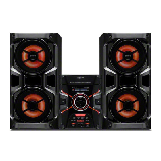
Photo: HCD-GPX8G (E2 Model)
Supported USB device
Mass Storage Class
Maximum current
500 mA
Disc player section
System
Compact disc and digital audio system
Laser Diode Properties
Emission Duration: Continuous
Laser Output*: Less than 44.6 μW
* This output is the value measurement
at a distance of 200 mm from the
objective lens surface on the Optical
Pick-up Block with 7 mm aperture.
Frequency response
20 Hz – 20 kHz
Signal-to-noise ratio
More than 90 dB
Dynamic range
More than 88 dB
Tuner section
FM stereo, FM/AM superheterodyne tuner
Antenna:
FM lead antenna
AM loop antenna
FM tuner section
Tuning range
87.5 MHz – 108.0 MHz (50 kHz step)
AM tuner section
Tuning range
Pan American models:
530 kHz – 1,710 kHz (10 kHz step)
531 kHz – 1,710 kHz (9 kHz step)
COMPACT DISC RECEIVER
E Model
NEW
CDM74I-DVBU201//M
CMS-ST6RFS3
Other models:
530 kHz – 1,610 kHz (10 kHz step)
531 kHz – 1,602 kHz (9 kHz step)
General
Power requirements
Mexican model: AC 120 V – 240 V, 60 Hz
Other models: AC 120 V – 240 V, 50/60 Hz
Power consumption
MHC-GPX8: 250 W
MHC-GPX7: 230 W
MHC-GPX5: 200 W
Dimensions (w/h/d) (excl. speakers)
(Approx.)
280 mm × 355 mm × 440 mm
Mass (excl. speakers) (Approx.)
HCD-GPX8G/HCD-GPX7G/
HCD-GPX5G: 7.0 kg
Supplied accessories
Remote control (1)
R6 (Size AA) batteries (2)
FM lead/AM loop antenna (1)
Spacer A (MHC-GPX8 only) (2)
Spacer B (MHC-GPX8 only) (2)
Speaker pads (MHC-GPX7 only) (8)
Design and specifi cations are subject to change
without notice.
Table of Contents

Related Manuals for Sony HCD-GPX5G


Summary of Contents for Sony HCD-GPX5G
- Page 1 All manuals and user guides at all-guides.com SERVICE MANUAL E Model Ver. 1.1 2012.07 • HCD-GPX5G is the amplifi er, USB, CD player and tuner section in MHC-GPX5. • HCD-GPX7G is the amplifi er, USB, CD player and tuner section in MHC-GPX7.
- Page 2 COMPONENTS IDENTIFIED BY MARK 0 OR DOTTED LINE WITH MARK 0 ON THE SCHEMATIC DIAGRAMS AND IN THE PARTS LIST ARE CRITICAL TO SAFE OPERATION. REPLACE THESE COMPONENTS WITH SONY PARTS WHOSE PART NUMBERS APPEAR AS SHOWN IN THIS MANUAL OR IN SUPPLEMENTS PUBLISHED BY SONY.
-
Page 3: Table Of Contents
All manuals and user guides at all-guides.com HCD-GPX5G/GPX7G/GPX8G TABLE OF CONTENTS 5-22. Printed Wiring Board - TUNER1AM3R Board ..... 45 SERVICING NOTES ..........5-23. Schematic Diagram - TUNER1AM3R Board - ....45 5-24. Printed Wiring Board - DMB22 Board - ......46 DISASSEMBLY 5-25. -
Page 4: Servicing Notes
HCD-GPX7G: E2, E51 4-411-595-1[] Unleaded solder has the following characteristics. • Unleaded solder melts at a temperature about 40 °C higher HCD-GPX5G: E2, E51 4-411-595-2[] than ordinary solder. HCD-GPX8G: MX 4-411-595-3[] Ordinary soldering irons can be used but the iron tip has to be... - Page 5 All manuals and user guides at all-guides.com HCD-GPX5G/GPX7G/GPX8G HOW TO OPEN THE TRAY WHEN POWER SWITCH TURN OFF CD mechanism deck (CDM74I) 1 Turn the gear to the direction of the arrow. (The location of this gear pulley is at the...
- Page 6 HCD-GPX5G/GPX7G/GPX8G All manuals and user guides at all-guides.com CAPACITOR DISCHARGE FOR ELECTRIC SHOCK PREVENTION in checking the DAMP 4CH board, make a capacitor for electrical shock prevention. C1431 4CH DAMP board board...
- Page 7 All manuals and user guides at all-guides.com HCD-GPX5G/GPX7G/GPX8G PRECAUTION WHEN INSTALLING A NEW OP UNIT/ PRECAUTION BEFORE UNSOLDERING THE STATIC ELECTRICITY PREVENTION SOLDER BRIDGE When installing a new OP unit, be sure to connect the fl exible printed circuit board fi rst of all before removing the static electric- ity prevention solder bridge by unsoldering.
-
Page 8: Disassembly
HCD-GPX5G/GPX7G/GPX8G All manuals and user guides at all-guides.com SECTION 2 DISASSEMBLY • This set can be disassembled in the order shown below. 2-1. DISASSEMBLY FLOW 2-2. CASE (Page 9) 2-3. LOADING PANEL 2-4. FRONT PANEL SECTION 2-5. CD MECHANISM SECTION... -
Page 9: Case
All manuals and user guides at all-guides.com HCD-GPX5G/GPX7G/GPX8G Note: Follow the disassembly procedure in the numerical order given. 2-2. CASE two screws (+BVTP 3x14) two screws 4 panel, side (L) (+BVTP 3x14) 4 panel, side (R) 1 two screws 2 two screws... -
Page 10: Front Panel Section
HCD-GPX5G/GPX7G/GPX8G All manuals and user guides at all-guides.com 2-4. FRONT PANEL SECTION 2 one screw (+BVTP 3x8) 2 one screw (+BVTP 3x8) 3 wire (flat type) (17core) CN601 4 CN707 (4P) 5 CN705 (10P) 1 one screws 1 four screws... -
Page 11: Tuner1Am3R Board
All manuals and user guides at all-guides.com HCD-GPX5G/GPX7G/GPX8G 2-6. TUNER1AM3R BOARD shield plate top TUNER1AM3R board shield plate bottom 1 wire (flat type) (9 core) (CN513) two screws (BVTP 3x8) 2-7. MAIN BOARD 1 two screws (+BVTP 3x8) 3 MAIN board... -
Page 12: Back Panel Section
HCD-GPX5G/GPX7G/GPX8G All manuals and user guides at all-guides.com 2-8. BACK PANEL SECTION 3 two screws 4 cover, fan (BVTP 3x8) 1 CN1405 (3P) 5 fan, DC 2 two screws (BVTP 3x8) 9 back panel section for GPX8G one screw (+BVTP 3x8) -
Page 13: 4Ch Damp Board
All manuals and user guides at all-guides.com HCD-GPX5G/GPX7G/GPX8G 2-9. 4CH DAMP BOARD 1 three screws (PTPWH 2.6x12) 3 two screws 3 two screws (BVTT 3x8) sheet thermal (BVTT 3x8) CN2 (9P) 6 4CH DAMP board 5 CN3 (5P) -
Page 14: Chassis Section
HCD-GPX5G/GPX7G/GPX8G All manuals and user guides at all-guides.com 2-10. CHASSIS SECTION 2 bracket, SMPS (shield) 1 two screws (+BVTP 3x8) two screws 5 nine screws (+BVTP 3x8) (+PWH 3x8) 6 REGULATOR, SWITCHING 7 chassis 3 CN1 (2P) -
Page 15: Cover Dust Cdm
All manuals and user guides at all-guides.com HCD-GPX5G/GPX7G/GPX8G 2-11. COVER DUST CDM 3 four screws (+BVTP 3x10) 4 bracket, holder (DMB) 5 go through the hole of cover dust 1 two screws (+BVTP 3x10) 1 two screws (+BVTP 3x10) 2 cover dust (CDM) 6 CDM74I 2-12. -
Page 16: Dmb22 Board
HCD-GPX5G/GPX7G/GPX8G All manuals and user guides at all-guides.com 2-13. DMB22 BOARD 2 clamp 1 four screws (+BVTP 3x10) 4 wire (flat type) (21core) (CN501) 5 DMB22 board 3 CN801 (6P) 6 bracket, holder (DMB) 7 CDM74I-DVBU201//M 2-14. DRIVER BOARD, SWITCH BOARD 1 two screws (+BTTP (M2.6)) -
Page 17: Sensor Board
All manuals and user guides at all-guides.com HCD-GPX5G/GPX7G/GPX8G 2-15. SENSOR BOARD 1 floating screw (+PTPWH M2.6) 2 tray 8 one screw (+BTTP (M2.6)) 3 belt (table) 0 SENSOR board 4 floating screw (+PTPWH M2.6) 5 pulley (table) 9 CN731 6 floating screw (3P) (+PTPWH M2.6) -
Page 18: Motor (Ld) Board
HCD-GPX5G/GPX7G/GPX8G All manuals and user guides at all-guides.com 2-17. MOTOR (LD) BOARD 3 two screws (+BTTP (M2.6)) 2 remove the two solderings of motor 5 MOTOR (LD) board 4 motor assy, loading (M751) 1 belt (loading) -
Page 19: Test Mode
All manuals and user guides at all-guides.com HCD-GPX5G/GPX7G/GPX8G SECTION 3 TEST MODE [PANEL TEST MODE] 4. When the [MASTER VOLUME] knob is turned clockwise even slightly, the sound volume increases to its maximum • This mode is used to check the fl uorescent indicator tube, and a message “VOLUME MAX”... - Page 20 HCD-GPX5G/GPX7G/GPX8G All manuals and user guides at all-guides.com [CD SHIP MODE (WITHOUT MEMORY CLEAR)] Press [ENTER] to Aging Display • This mode moves the optical pick-up to the position du- • To release from Meter Aging Mode. rable to vibration. Use this mode when returning the set to...
- Page 21 All manuals and user guides at all-guides.com HCD-GPX5G/GPX7G/GPX8G Defect of AMP circuit 1-1. If PROTECT mode is “AMPLIFIER”, The following defect might be possible. Defects Possible cause Unusual heat up of MOSFET by im- OTP (Over Tempera- proper assembly of heatsink, destruction ture Protection) of MOSFET etc..
-
Page 22: Electrical Check
HCD-GPX5G/GPX7G/GPX8G All manuals and user guides at all-guides.com SECTION 4 ELECTRICAL CHECK CD SECTION 0 dB = 1 μV TUNER SECTION FM AUTO STOP CHECK Note: 1. CD Block is basically constructed to operate without adjustment. signal 2. Use YEDS-18 disc (Part No. 3-702-101-01) unless otherwise indicat- generator 3. -
Page 23: Diagrams
All manuals and user guides at all-guides.com HCD-GPX5G/GPX7G/GPX8G SECTION 5 DIAGRAMS 5-1. BLOCK DIAGRAM – CD/USB Section – ASYNCHRONOUS SAMPLE MULTIPLEXER RATE CONVERTER D/A CONVERTER IC741 IC761 IC762 IC763 L-OUT (Page 24) SDIN SDOUT SDIN1 VOUT L ASDATA0 1 18... -
Page 24: Block Diagram - Main Section
All manuals and user guides at all-guides.com HCD-GPX5G/GPX7G/GPX8G 5-2. BLOCK DIAGRAM – MAIN Section – OP AMP IC901 L-OUT (Page 23) 39 GAME_L L-IN (Page 23) INGAIN OUT L INGAIN OUT R R-CH AUDIO IN J500 43 GAME-LEFT R-CH GAME... -
Page 25: Block Diagram - Amp Section
All manuals and user guides at all-guides.com HCD-GPX5G/GPX7G/GPX8G 5-3. BLOCK DIAGRAM – AMP Section – GPX8G POWER AMP IC1406 GPX8G GPX7G GPX5G GPX8G BOOSTER SW BPF-L TB1400 TB1400 Q1422 IC900 SW OUT L INPUT+ OUTPUT INA- AOUT CLOCK (Page 24) -
Page 26: Block Diagram - Panel/Power Supply Section
All manuals and user guides at all-guides.com HCD-GPX5G/GPX7G/GPX8G 5-4. BLOCK DIAGRAM – PANEL/POWER SUPPLY Section – +13V SEL A : DISPLAY BOARD D1008, D1009, D1012, D1013, D1016, D1017, D1018, D1019, D1022, D1023, D1027 DINAMIC LED LED +13.5V (SEL A) GR15... - Page 27 All manuals and user guides at all-guides.com HCD-GPX5G/GPX7G/GPX8G THIS NOTE IS COMMON FOR PRINTED WIRING BOARDS AND SCHEMATIC DIAGRAMS. • Circuit Boards Location (In addition to this, the necessary note is printed in each block.) For Printed Wiring Boards. For Schematic Diagrams.
-
Page 28: 4Ch Damp Board (Component Side)
All manuals and user guides at all-guides.com HCD-GPX5G/GPX7G/GPX8G Ver. 1.1 PRINTED WIRING BOARD – 4CH DAMP Board (Component side) – • 5-5. • See page 27 for Circuit Boards Location. : Uses unleaded solder. 4CH DAMP BOARD (Component Side) MAIN... -
Page 29: 4Ch Damp Board (Conductor Side)
All manuals and user guides at all-guides.com HCD-GPX5G/GPX7G/GPX8G Ver. 1.1 PRINTED WIRING BOARD – 4CH DAMP Board (Conductor side) – • 5-6. • See page 27 for Circuit Boards Location. : Uses unleaded solder. 4CH DAMP BOARD (Conductor Side) JL1451... -
Page 30: Schematic Diagram - 4Ch Damp Board (1/3)
All manuals and user guides at all-guides.com HCD-GPX5G/GPX7G/GPX8G Ver. 1.1 5-7. SCHEMATIC DIAGRAM – 4CH DAMP Board (1/3) – 4CH DAMP BOARD (1/3) GPX8G C1415 C1456 R1424 R1435 2.7k JL1436 JL1444 JL1432 JL1442 R1410 100k CN1400 R1436 R1447 R1458 C1460... -
Page 31: Schematic Diagram - 4Ch Damp Board (2/3)
All manuals and user guides at all-guides.com HCD-GPX5G/GPX7G/GPX8G 5-8. SCHEMATIC DIAGRAM – 4CH DAMP Board (2/3) – • See page 51 for IC Block Diagrams. 4CH DAMP BOARD (2/3) IC1406 IC B/D GPX8G R1546 Q1422 IC1406 R1502 C1482 220p IRF6775MTR1PBF... -
Page 32: Schematic Diagram - 4Ch Damp Board (3/3)
All manuals and user guides at all-guides.com HCD-GPX5G/GPX7G/GPX8G 5-9. SCHEMATIC DIAGRAM – 4CH DAMP Board (3/3) – 4CH DAMP BOARD (3/3) GPX8G TB1400 R1762 R1765 GPX7G/8G TB1400 TB1400 GPX8G GPX7G GPX7G GPX8G JL1489 C1585 1000p TB1403 R1763 R1764 C1658 L1406 0.01uH... -
Page 33: Printed Wiring Board - Display Board
All manuals and user guides at all-guides.com HCD-GPX5G/GPX7G/GPX8G 5-10. PRINTED WIRING BOARD – DISPLAY Board – • • See page 27 for Circuit Boards Location. : Uses unleaded solder. DISPLAY BOARD JR1018 TP1057 JR JR1052 TP1058 C1064 TP1043 TP1042 C1059... -
Page 34: Schematic Diagram - Display Board
All manuals and user guides at all-guides.com HCD-GPX5G/GPX7G/GPX8G 5-11. SCHEMATIC DIAGRAM – DISPLAY Board – • See page 50 for Waveforms. • See page 51 for IC Block Diagrams. DISPLAY BOARD FL1001 TP1041 TP1040 IC1003 C1028 100p IC1003 PNA4823M03S0 REMOTE CONTROL... -
Page 35: Main Board (Component Side)
All manuals and user guides at all-guides.com HCD-GPX5G/GPX7G/GPX8G Ver. 1.1 5-12. PRINTED WIRING BOARD – MAIN Board (Component side) – • • See page 27 for Circuit Boards Location. : Uses unleaded solder. MAIN BOARD (Component side) 4CH DAMP BOARD... -
Page 36: Main Board (Conductor Side)
All manuals and user guides at all-guides.com HCD-GPX5G/GPX7G/GPX8G 5-13. PRINTED WIRING BOARD – MAIN Board (Conductor side) – • • See page 27 for Circuit Boards Location. : Uses unleaded solder. MAIN BOARD (Conductor side) (13) 1-885-680- HCD-GPX5G/GPX7G/GPX8G... -
Page 37: Schematic Diagram - Main Board (1/4)
All manuals and user guides at all-guides.com HCD-GPX5G/GPX7G/GPX8G 5-14. SCHEMATIC DIAGRAM – MAIN Board (1/4) – • See page 50 for Waveforms • See page 51 for IC Block Diagrams. • See page 56 for IC Pin Function Descriptions. MAIN BOARD (1/4) -
Page 38: Schematic Diagram - Main Board (2/4)
All manuals and user guides at all-guides.com HCD-GPX5G/GPX7G/GPX8G Ver. 1.1 5-15. SCHEMATIC DIAGRAM – MAIN Board (2/4) – • See page 51 for IC Block Diagrams. DMB22 BOARD (1/3) CN702 (Page 47) MAIN BOARD (1/4) (Page 37) CN702 IC901 BA4558F-E2... -
Page 39: Schematic Diagram - Main Board (3/4)
All manuals and user guides at all-guides.com HCD-GPX5G/GPX7G/GPX8G 5-16. SCHEMATIC DIAGRAM – MAIN Board (3/4) – MAIN BOARD (1/4) (Page 37) MAIN BOARD (3/4) IC801 C813 C812 BD9328EFJ-E2 3300p C809 R766 +3.3V REG R849 7.5k JL975 GPX7G/8G R781 CN800 Q704 13.5... -
Page 40: Schematic Diagram - Main Board (4/4)
All manuals and user guides at all-guides.com HCD-GPX5G/GPX7G/GPX8G 5-17. SCHEMATIC DIAGRAM – MAIN Board (4/4) – • See page 50 for Waveforms • See page 51 for IC Block Diagrams. MAIN BOARD (2/4) (Page 38) 39 40 41 42 43 44 45 46 47 48 49... -
Page 41: Printed Wiring Board - Usb, Volume And Mic Board
All manuals and user guides at all-guides.com HCD-GPX5G/GPX7G/GPX8G 5-18. PRINTED WIRING BOARD – USB, VOLUME AND MIC Board – • • See page 27 for Circuit Boards Location. : Uses unleaded solder. VOLUME BOARD S1181 USB BOARD S1182 TP1185 TUNING +... -
Page 42: Schematic Diagram - Usb, Volume And Mic Board
All manuals and user guides at all-guides.com HCD-GPX5G/GPX7G/GPX8G 5-19. SCHEMATIC DIAGRAM – USB, VOLUME AND MIC Board – USB BOARD VOLUME BOARD NO1200 TP1181 DISPLAY BOARD TP1182 CN1002 DGND TP1183 (Page 34) ADKEY0 S1250 ET1202 S1180 TP1226 DJ CONTROL/ TUNING –... -
Page 43: Printed Wiring Board - Driver, Sensor, Switch, Motor (Ld) And Motor (Tb) Board
All manuals and user guides at all-guides.com HCD-GPX5G/GPX7G/GPX8G 5-20. PRINTED WIRING BOARD – DRIVER, SENSOR, SWITCH, MOTOR (LD) AND MOTOR (TB) Board – • • See page 27 for Circuit Boards Location. : Uses unleaded solder. MOTOR (LD) BOARD DRIVER BOARD... -
Page 44: Schematic Diagram - Driver, Sensor, Switch, Motor (Ld) And Motor (Tb) Board
All manuals and user guides at all-guides.com HCD-GPX5G/GPX7G/GPX8G 5-21. SCHEMATIC DIAGRAM – DRIVER, SENSOR, SWITCH, MOTOR (LD) AND MOTOR (TB) Board – • See page 51 for IC Block Diagrams. DRIVER BOARD IC B/D IC701 IC701 BA6956AN LD MOTOR DRIVER 0 0.2... -
Page 45: Printed Wiring Board - Tuner1Am3R Board
All manuals and user guides at all-guides.com HCD-GPX5G/GPX7G/GPX8G 5-22. PRINTED WIRING BOARD – TUNER1AM3R Board – 5-23. SCHEMATIC DIAGRAM – TUNER1AM3R Board – • See page 51 for IC Block Diagrams. • See page 27 for Circuit Boards Location. •... -
Page 46: Printed Wiring Board - Dmb22 Board
All manuals and user guides at all-guides.com HCD-GPX5G/GPX7G/GPX8G 5-24. PRINTED WIRING BOARD – DMB22 Board – • • See page 27 for Circuit Boards Location. : Uses unleaded solder. DMB22 BOARD (Component side) DMB22 BOARD (Conductor side) FOR TEST C712... -
Page 47: Schematic Diagram - Dmb22 Board (1/3)
All manuals and user guides at all-guides.com HCD-GPX5G/GPX7G/GPX8G 5-25. SCHEMATIC DIAGRAM – DMB22 Board (1/3) – • See page 50 for Waveforms • See page 51 for IC Block Diagrams. DMB22 BOARD (3/3) MTR_GND R701 (Page 49) DMB22 BOARD (1/3) -
Page 48: Schematic Diagram - Dmb22 Board (2/3)
All manuals and user guides at all-guides.com HCD-GPX5G/GPX7G/GPX8G 5-26. SCHEMATIC DIAGRAM – DMB22 Board (2/3) – • See page 50 for Waveforms. • See page 51 for IC Block Diagrams. • See page 56 for IC Pin Function Descriptions. DMB22 BOARD... -
Page 49: Schematic Diagram - Dmb22 Board (3/3)
All manuals and user guides at all-guides.com HCD-GPX5G/GPX7G/GPX8G 5-27. SCHEMATIC DIAGRAM – DMB22 Board (3/3) – • See page 51 for IC Block Diagrams. DMB22 BOARD (3/3) DMB22 DVDD5V BOARD DGND (1/3),(2/3) DMB22 (Page 47) DVDD3.3V RF+3.3V BOARD (Page 48) - Page 50 HCD-GPX5G/GPX7G/GPX8G All manuals and user guides at all-guides.com • Waveforms – DMB22 Board – – MAIN Board – – DISPLAY Board – IC501 8 (XTALO) IC500 qa (XC-OUT) IC1001 7 (OSC) 151.7 mVp-p 196.7 mVp-p 148.3 mVp-p 2.73 s 30.6 s 37.6 ns...
- Page 51 All manuals and user guides at all-guides.com HCD-GPX5G/GPX7G/GPX8G • IC Block Diagrams IC1405 NJM2903V (TE2) (4CH DAMP BOARD (2/3)) IC1410, IC1411 BA4580RF-E2 (4CH DAMP BOARD (2/3)) IC702 NJM2903V (TE2) (MAIN BOARD (4/4)) – IC1406, IC1407, IC1408, IC1409 IRS2092STRPBF (4CH DAMP BOARD)
- Page 52 HCD-GPX5G/GPX7G/GPX8G All manuals and user guides at all-guides.com IC1001 PT6324-LQ (DISPLAY BOARD) CONTROL SERIAL DISPLAY DATA MEMORY INTERFACE DOUT SEGMENT DRIVER TIMING GENERATOR KEY MATRIX MEMORY SG24 GRID SG23 DRIVER DIMMING SG22 CIRCUIT SG1/KS1 SG21 SG2/KS2 SG20 SG3/KS3 SG19 SG4/KS4...
- Page 53 All manuals and user guides at all-guides.com HCD-GPX5G/GPX7G/GPX8G IC761 IC SRC4182 (DMB22 BOARD) REFERENCE INTERPOLATION DECIMATION RCKI RE-SAMPLER CLOCK FILTERS FILTERS 28 MODE2 SDIN 27 MODE1 AUDIO BCKI INPUT 26 MODE0 PORT LRCKI RATE ESTIMATOR 25 BCKO AUDIO 24 LRCKO...
- Page 54 HCD-GPX5G/GPX7G/GPX8G All manuals and user guides at all-guides.com IC801 BD8203EFV-E2 (DMB22 Board (3/3)) SGND 1 SGND SGND SGND OPVCC REG5 2 REGVAR SGND SGND PREVCC REGVARVCC PREVCC PVCC1 4 REGCTL STBY REGRST PGND PGND TSDM VO1+ 6 LEVEL MUTE4 MUTE4 SHIFT VO1–...
- Page 55 All manuals and user guides at all-guides.com HCD-GPX5G/GPX7G/GPX8G IC806 R2A15216FP (MAIN BOARD (2/4)) REFERENCE INDR INDL 6 INPUT 6 INPUT INER SELECTOR SELECTOR INEL (R-CH) (L-CH) INFR INFL GAMER GAMEL INGAINOUTR INGAINOUTL RECAR RECAL RECBR RECBL VOCAL CUT SURROUND OR DPL IN...
- Page 56 HCD-GPX5G/GPX7G/GPX8G All manuals and user guides at all-guides.com • IC Pin Function Description MAIN BOARD (1/4) IC500 R5F3650KBDFA Pin No. Pin Name Description LED-DATA Data output pin to LED driver LED-CLK Clock output pin to LED driver FR-SPK-LED-RED PWM output to front speaker RED LED (Only for HCD-GPX7 and HCD-GPX8)
- Page 57 All manuals and user guides at all-guides.com HCD-GPX5G/GPX7G/GPX8G Pin No. Pin Name Description NO-USE Not Used NO-USE Not Used NO-USE Not Used NO-USE Not Used /FAN-BLOCK DET Fan Block Detection Input Pin. "L": Block On Power supply terminal (+3.3V) PCONT-7V-13.5V 13.5V &...
- Page 58 HCD-GPX5G/GPX7G/GPX8G All manuals and user guides at all-guides.com DMB22 BOARD (2/3) IC501 CXD90013R Pin No. Pin Name Description RF main beam (A) input from the optical pick-up block RF main beam (D) input from the optical pick-up block RF sub beam (F) input from the optical pick-up block...
- Page 59 All manuals and user guides at all-guides.com HCD-GPX5G/GPX7G/GPX8G Pin No. Pin Name Description Two-way data bus with the SD-RAM DQM0 Data mask signal output to the SD-RAM RD15 Two-way data bus with the SD-RAM RD14 Two-way data bus with the SD-RAM...
- Page 60 HCD-GPX5G/GPX7G/GPX8G All manuals and user guides at all-guides.com Pin No. Pin Name Description ADACVDD1 Power supply terminal (+3.3V) ADACVDD2 Power supply terminal (+3.3V) AVDD12_1 Power supply terminal (+1.2V) AGND12 Ground terminal RFIP AC coupled RF signal input from the optical pick-up block...
-
Page 61: Exploded Views
All manuals and user guides at all-guides.com HCD-GPX5G/GPX7G/GPX8G SECTION 6 EXPLODED VIEWS Note: • -XX and -X mean standardized parts, so • Color Indication of Appearance Parts Ex- The components identifi ed by mark 0 they may have some difference from the... -
Page 62: Front Panel Section
HCD-GPX5G/GPX7G/GPX8G All manuals and user guides at all-guides.com Ver. 1.1 6-2. FRONT PANEL SECTION not supplied (DISPLAY board) FL1001 not supplied (VOLUME board) not supplied not supplied (MIC board) (for GPX7G/ GPX8G only) not supplied not supplied (for GPX7G/GPX8G only) Note: If wire (fl... -
Page 63: Back Panel Section
All manuals and user guides at all-guides.com HCD-GPX5G/GPX7G/GPX8G 6-3. BACK PANEL SECTION not supplied TUNER1AM3R board not supplied CD mechanism section (1) (for GPX8G only) Note: If wire (fl at type) is replaced, install it after bending it in the same form as that before replacement. -
Page 64: Chassis Section
HCD-GPX5G/GPX7G/GPX8G All manuals and user guides at all-guides.com Ver. 1.1 6-4. CHASSIS SECTION not supplied not supplied not supplied Ref. No. Part No. Description Remark Ref. No. Part No. Description Remark 4-435-965-01 SCREW +PTPWH 2.6XL (DIA.8.0) 0 155 1-569-007-12 ADAPTOR, CONVERSION 2P (E2) -
Page 65: Cd Mechanism Section (1) (Cdm74I-Dvbu201//M)
All manuals and user guides at all-guides.com HCD-GPX5G/GPX7G/GPX8G 6-5. CD MECHANISM SECTION (1) (CDM74I-DVBU201//M) not supplied (SENSOR board) CD mechanism section 2 M741 not supplied (MOTOR (TB) board) not supplied not supplied Ref. No. Part No. Description Remark Ref. No. -
Page 66: Cd Mechanism Section (2)
HCD-GPX5G/GPX7G/GPX8G All manuals and user guides at all-guides.com Ver. 1.1 6-6. CD MECHANISM SECTION (2) RE701 not supplied (MOTOR, LD board) M751 supplied not supplied (SWITCH board) not supplied Ref. No. Part No. Description Remark Ref. No. Part No. Description... -
Page 67: Electrical Parts List
All manuals and user guides at all-guides.com HCD-GPX5G/GPX7G/GPX8G SECTION 7 4CH DAMP ELECTRICAL PARTS LIST Note: • Due to standardization, replacements in • CAPACITORS When indicating parts by reference num- the parts list may be different from the uF: μF ber, please include the board name. - Page 68 HCD-GPX5G/GPX7G/GPX8G All manuals and user guides at all-guides.com Ver. 1.1 4CH DAMP Ref. No. Part No. Description Remark Ref. No. Part No. Description Remark C1506 1-107-726-91 CERAMIC CHIP 0.01uF C1574 1-100-566-91 CERAMIC CHIP 0.1uF C1578 1-127-820-11 CERAMIC CHIP 4.7uF C1507 1-107-726-91 CERAMIC CHIP 0.01uF...
- Page 69 6-551-690-01 TRANSISTOR RT3N11M-TP-1 D1422 6-502-945-01 DI CRH01 (TE85R, Q) (GPX8G) Q1405 6-551-690-01 TRANSISTOR RT3N11M-TP-1 D1423 6-503-775-01 DI CRH02 (T5R, SONY, XM) Q1407 6-551-693-01 TRANSISTOR RT3T11M-TP-1 D1424 6-503-775-01 DI CRH02 (T5R, SONY, XM) D1425 6-503-775-01 DI CRH02 (T5R, SONY, XM) Q1410...
- Page 70 HCD-GPX5G/GPX7G/GPX8G All manuals and user guides at all-guides.com Ver. 1.1 4CH DAMP Ref. No. Part No. Description Remark Ref. No. Part No. Description Remark R1420 1-216-825-11 METAL CHIP 2.2K 1/10W R1463 1-216-793-11 METAL CHIP 1/10W (GPX7G) R1464 1-216-793-11 METAL CHIP...
- Page 71 All manuals and user guides at all-guides.com HCD-GPX5G/GPX7G/GPX8G Ver. 1.1 4CH DAMP Ref. No. Part No. Description Remark Ref. No. Part No. Description Remark R1515 1-218-958-11 METAL CHIP 2.7K 1/16W R1567 1-216-801-11 METAL CHIP 1/10W (GPX8G) (GPX8G) R1516 1-208-905-11 METAL CHIP 5.6K...
- Page 72 HCD-GPX5G/GPX7G/GPX8G All manuals and user guides at all-guides.com Ver. 1.1 4CH DAMP DISPLAY Ref. No. Part No. Description Remark Ref. No. Part No. Description Remark R1663 1-208-695-11 METAL CHIP 3.3K 0.5% 1/16W R1781 1-227-869-21 METAL CHIP 1/2W R1782 1-227-869-21 METAL CHIP...
- Page 73 < FLUORESCENT INDICATOR TUBE > < DIODE > FL1001 1-483-424-11 VACUUM FLUORESCENT DISPLAY D1001 6-502-970-01 DI DZ2J068M0L D1002 6-503-775-01 DI CRH02 (T5R, SONY, XM) < IC > D1003 6-503-775-01 DI CRH02 (T5R, SONY, XM) D1004 6-503-775-01 DI CRH02 (T5R, SONY, XM) IC1001 6-717-584-01...
- Page 74 HCD-GPX5G/GPX7G/GPX8G All manuals and user guides at all-guides.com Ver. 1.1 DISPLAY DMB22 Ref. No. Part No. Description Remark Ref. No. Part No. Description Remark JR1061 1-216-296-11 SHORT CHIP R1047 1-257-173-91 METAL CHIP 1/3W JR1062 1-216-296-11 SHORT CHIP R1048 1-257-173-91 METAL CHIP...
- Page 75 All manuals and user guides at all-guides.com HCD-GPX5G/GPX7G/GPX8G Ver. 1.1 DMB22 Ref. No. Part No. Description Remark Ref. No. Part No. Description Remark C516 1-112-777-11 CERAMIC CHIP 0.01uF C768 1-164-850-11 CERAMIC CHIP 10PF 0.5PF C517 1-112-777-11 CERAMIC CHIP 0.01uF C769...
- Page 76 HCD-GPX5G/GPX7G/GPX8G All manuals and user guides at all-guides.com Ver. 1.1 DMB22 Ref. No. Part No. Description Remark Ref. No. Part No. Description Remark FB721 1-469-092-11 FERRITE, EMI (SMD) (1608) R554 1-218-941-81 METAL CHIP 1/16W FB722 1-469-092-11 FERRITE, EMI (SMD) (1608)
- Page 77 All manuals and user guides at all-guides.com HCD-GPX5G/GPX7G/GPX8G Ver. 1.1 DMB22 DRIVER MAIN Ref. No. Part No. Description Remark Ref. No. Part No. Description Remark R760 1-218-937-11 METAL CHIP 1/16W < VIBRATOR > R762 1-218-990-81 SHORT CHIP R763 1-218-941-81 METAL CHIP...
- Page 78 HCD-GPX5G/GPX7G/GPX8G All manuals and user guides at all-guides.com Ver. 1.1 MAIN Ref. No. Part No. Description Remark Ref. No. Part No. Description Remark C508 1-114-553-11 CERAMIC CHIP 10uF C739 1-164-874-11 CERAMIC CHIP 100PF C509 1-114-817-11 CERAMIC CHIP 2.2uF C740 1-100-597-91 CERAMIC CHIP 0.1uF...
- Page 79 All manuals and user guides at all-guides.com HCD-GPX5G/GPX7G/GPX8G Ver. 1.1 MAIN Ref. No. Part No. Description Remark Ref. No. Part No. Description Remark C856 1-137-765-21 ELECT CHIP 47uF C963 1-100-597-91 CERAMIC CHIP 0.1uF C966 1-124-779-00 ELECT CHIP 10uF C857 1-100-579-81 CERAMIC CHIP 0.0056uF...
- Page 80 HCD-GPX5G/GPX7G/GPX8G All manuals and user guides at all-guides.com Ver. 1.1 MAIN Ref. No. Part No. Description Remark Ref. No. Part No. Description Remark CN601 1-843-189-21 CONNECTOR, FLEXIBLE 17P IC803 6-715-078-01 IC KIA7809AF/API CN700 1-784-023-51 CONNECTOR, FLEXIBLE 13P IC804 6-703-639-01 IC TK11140CSCL-G...
- Page 81 All manuals and user guides at all-guides.com HCD-GPX5G/GPX7G/GPX8G Ver. 1.1 MAIN Ref. No. Part No. Description Remark Ref. No. Part No. Description Remark R535 1-218-941-81 METAL CHIP 1/16W R703 1-218-941-81 METAL CHIP 1/16W R704 1-218-965-31 METAL CHIP 1/16W R536 1-218-941-81...
- Page 82 HCD-GPX5G/GPX7G/GPX8G All manuals and user guides at all-guides.com Ver. 1.1 MAIN Ref. No. Part No. Description Remark Ref. No. Part No. Description Remark R794 1-216-820-11 METAL CHIP 1/10W R913 1-216-845-11 METAL CHIP 100K 1/10W (GPX8G) (GPX8G) R914 1-218-971-11 METAL CHIP...
- Page 83 All manuals and user guides at all-guides.com HCD-GPX5G/GPX7G/GPX8G Ver. 1.1 MAIN Ref. No. Part No. Description Remark Ref. No. Part No. Description Remark R967 1-216-833-11 METAL CHIP 1/10W R1014 1-216-820-11 METAL CHIP 1/10W R968 1-218-955-11 METAL CHIP 1.5K 1/16W (GPX8G)
- Page 84 HCD-GPX5G/GPX7G/GPX8G All manuals and user guides at all-guides.com MOTOR (TB) MOTOR (LD) SENSOR SWITCH TUNER1AM3R Ref. No. Part No. Description Remark Ref. No. Part No. Description Remark < DIODE > SENSOR BOARD ************* D1300 6-500-848-01 DIODE MC2840-T112-1 D1301 6-502-961-01 DI DA2J10100L <...
- Page 85 All manuals and user guides at all-guides.com HCD-GPX5G/GPX7G/GPX8G TUNER1AM3R VOLUME Ref. No. Part No. Description Remark Ref. No. Part No. Description Remark < RESISTOR > D1224 6-503-224-02 DI 1L0352V22F3MIT02 (GPX5G/GPX7G) D1224 6-503-720-01 DI 1L0353W61B3MKT01 (GPX8G) R101 1-216-809-11 METAL CHIP 1/10W...
- Page 86 HCD-GPX5G/GPX7G/GPX8G All manuals and user guides at all-guides.com Ver. 1.1 Ref. No. Part No. Description Remark Ref. No. Part No. Description Remark MISCELLANEOUS ************** 1-828-995-11 WIRE (FLAT TYPE) (17 CORE) 0 102 1-855-006-11 FAN, DC 1-838-606-11 WIRE (FLAT TYPE) (9 CORE)
- Page 87 HCD-GPX5G/GPX7G/GPX8G All manuals and user guides at all-guides.com E Model SERVICE MANUAL Ver. 1.1 2012.07 SUPPLEMENT-1 File this supplement with the service manual. Subject: Addition of SERVICING NOTES (TROUBLESHOOTING) 9-890-600-81...
- Page 88 HCD-GPX5G/GPX7G/GPX8G All manuals and user guides at all-guides.com SECTION 1 SERVICING NOTES...
- Page 89 All manuals and user guides at all-guides.com HCD-GPX5G/GPX7G/GPX8G...
- Page 90 HCD-GPX5G/GPX7G/GPX8G All manuals and user guides at all-guides.com...
- Page 91 All manuals and user guides at all-guides.com HCD-GPX5G/GPX7G/GPX8G...
- Page 92 HCD-GPX5G/GPX7G/GPX8G All manuals and user guides at all-guides.com...
- Page 93 All manuals and user guides at all-guides.com HCD-GPX5G/GPX7G/GPX8G...
- Page 94 HCD-GPX5G/GPX7G/GPX8G All manuals and user guides at all-guides.com REVISION HISTORY Checking the version allows you to jump to the revised page. Also, clicking the version at the top of the revised page allows you to jump to the next revised page.