Table of Contents
Quick Links
Table of Contents

Related Manuals for Asus AAEON EPIC-KBS7


Summary of Contents for Asus AAEON EPIC-KBS7
- Page 1 EPIC-KBS7 EPIC Board User’s Manual 4 Last Updated: March 25, 2021...
- Page 2 Copyright Notice This document is copyrighted, 2021. All rights are reserved. The original manufacturer reserves the right to make improvements to the products described in this manual at any time without notice. No part of this manual may be reproduced, copied, translated, or transmitted in any form or by any means without the prior written permission of the original manufacturer.
- Page 3 Acknowledgement All other products’ name or trademarks are properties of their respective owners. Microsoft Windows® is a registered trademark of Microsoft Corp. ⚫ Intel® and Celeron® are registered trademarks of Intel Corporation ⚫ Intel Core™ is a trademark of Intel Corporation ⚫...
- Page 4 Packing List Before setting up your product, please make sure you have received the following items: Item Quantity EPIC-KBS7 ⚫ SATA power cable P/N: 1702150155 ⚫ SATA cable P/N: 1709070500 ⚫ Jumper cap P/N: 9657666600 ⚫ If any of these items are missing or damaged, please contact your distributor or sales representative immediately.
- Page 5 About this Document This User’s Manual contains all the essential information, such as detailed descriptions and explanations on the product’s hardware and software features (if any), its specifications, dimensions, jumper/connector settings and definitions, and driver installation instructions (if any), to facilitate users in setting up their product. Users may refer to the product page at AAEON.com for the latest version of this document.
- Page 6 Safety Precautions Please read the following safety instructions carefully. It is advised that you keep this manual for future references All cautions and warnings on the device should be noted. Make sure the power source matches the power rating of the device. Position the power cord so that people cannot step on it.
- Page 7 If any of the following situations arises, please the contact our service personnel: Damaged power cord or plug Liquid intrusion to the device iii. Exposure to moisture Device is not working as expected or in a manner as described in this manual The device is dropped or damaged Any obvious signs of damage displayed on the device...
- Page 8 FCC Statement This device complies with Part 15 FCC Rules. Operation is subject to the following two conditions: (1) this device may not cause harmful interference, and (2) this device must accept any interference received including interference that may cause undesired operation.
- Page 9 China RoHS Requirements (CN) 产品中有毒有害物质或元素名称及含量 AAEON Main Board/ Daughter Board/ Backplane 有毒有害物质或元素 部件名称 铅 汞 镉 六价铬 多溴联苯 多溴二苯醚 (Pb) (Hg) (Cd) (Cr(VI)) (PBB) (PBDE) 印刷电路板 ○ ○ ○ ○ ○ ○ 及其电子组件 外部信号 ○ ○ ○ ○ ○ ○ 连接器及线材...
- Page 10 China RoHS Requirement (EN) Poisonous or Hazardous Substances or Elements in Products AAEON Main Board/ Daughter Board/ Backplane Poisonous or Hazardous Substances or Elements Hexavalent Polybrominated Polybrominated Component Lead Mercury Cadmium Chromium Biphenyls Diphenyl Ethers (Pb) (Hg) (Cd) (Cr(VI)) (PBB) (PBDE) PCB &...
-
Page 11: Table Of Contents
Table of Contents Chapter 1 - Product Specifications..................1 Specifications ......................2 Chapter 2 – Hardware Information ..................4 Dimensions ....................... 5 Jumpers and Connectors ..................8 List of Jumpers ......................10 2.3.1 LVDS Power Select/ LVDS BKLT Power Select (JP4) ......10 2.3.2 LVDS Backlight Brightness Control Mode Select (JP5) ...... - Page 12 2.4.15 COM3 RS232 Pin Header (CN18) ............22 2.4.16 DIO PIN HEADER (CN24) ................. 23 2.4.17 COM4 RS232 Pin Header (CN26) ............23 CPU Installation ...................... 24 Chapter 3 - BIOS Setup ......................27 System Test and Initialization ................28 AMI BIOS Setup .....................
- Page 13 Driver Download and Installation............... 55 Appendix A - Watchdog Timer Programming ..............57 Watchdog Timer Initial Program ................ 58 Appendix B - I/O Information ....................63 I/O Address Map ....................64 Memory Address Map ..................66 IRQ Mapping Chart ....................68 Appendix C –...
-
Page 14: Chapter 1 - Product Specifications
Chapter 1 Chapter 1 - Product Specifications... -
Page 15: Specifications
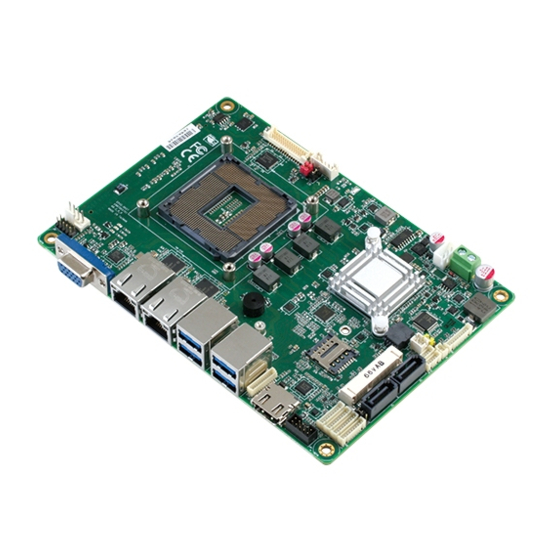
Specifications System Form Factor 4” EPIC Board 6th/7th Generation Intel® CPU (Socket Type, TDP 35W, 54W Only) CPU Frequency 6th/7th Generation Intel® Core™ i3/ i5/ i7/ Celeron® Chipset H110, Q170 (6W) Memory Type DDR4 (Non-ECC), 2133MHz Max. Memory Capacity Up to 16GB BIOS Wake on LAN Watchdog Timer... - Page 16 Display VGA/LCD Controller 6th/7th Generation Intel® Core™ i3/ i5/ i7/ Celeron® Video Output CRT/ LVDS/ HDMI Backlight Inverter Supply Max. 12V Ethernet LAN x 2 (Rear IO) (i211 x 2) Audio ALC892, no Amp USB Port USB3.2 Gen 1 x 4 (Rear IO) USB2.0 x 2 (Internal) Serial Port COM x 4 (COM2: RS-232/422/485)
-
Page 17: Chapter 2 - Hardware Information
Chapter 2 Chapter 2 – Hardware Information... -
Page 18: Dimensions
Dimensions Component Side Chapter 2 – Hardware Information... - Page 19 Side View with Thermal Solution Chapter 2 – Hardware Information...
- Page 20 Solder Side Chapter 2 – Hardware Information...
-
Page 21: Jumpers And Connectors
Jumpers and Connectors Component Side Chapter 2 – Hardware Information... - Page 22 Solder Side Chapter 2 – Hardware Information...
-
Page 23: List Of Jumpers
List of Jumpers Please refer to the table below for all of the board’s jumpers that you can configure for your application Label Function LVDS Power Select/ LVDS BKLT Power Select LVDS Backlight Brightness Control Mode Select Clear CMOS AT/ATX Select Front Panel PIN Header 2.3.1 LVDS Power Select/ LVDS BKLT Power Select (JP4) -
Page 24: Lvds Backlight Brightness Control Mode Select (Jp5)
2.3.2 LVDS Backlight Brightness Control Mode Select (JP5) VR Mode PWM Mode (Default) 2.3.3 Clear CMOS (JP6) 1 2 3 Normal (Default) Clear CMOS 2.3.4 AT/ATX Select (JP7) 1 2 3 ATX Mode AT Mode (Default) Chapter 2 – Hardware Information... -
Page 25: Front Panel Header (Jp9)
2.3.5 Front Panel Header (JP9) Pin Name Pin Name EXT_PWRBTN# FP_HDLED- FP_HDLED+ FP_SPKR- +V5S PWRLED+ HWRST# Chapter 2 – Hardware Information... -
Page 26: List Of Connectors
List of Connectors Please refer to the table below for all of the board’s connectors that you can configure for your application Label Function PC Buzzer Backlight Connector 2-Pin DC IN Connector LVDS Connector 3-Pin SB Power IN Connector Audio Pin Header RTC Battery Connector SATA Power Connector USB2.0 Connector... -
Page 27: Backlight Connector (Cn1)
Label Function CN23 HDMI Connector CN24 DIO Connector CN25 VGA Connector CN26 COM4 RS232 Pin Header CPU1 CPU Socket DIMM1 RAM Socket 1 LED1 Standby Power LED Indicator LED2 +V5S LED Indicator LED3 HDD LED Indicator BOIS Socket 2.4.1 Backlight Connector (CN1) Pin Name Max Current BLK_PWR... -
Page 28: 2-Pin Dc In Connector (Cn2)
2.4.2 2-Pin DC IN Connector (CN2) Pin Name +VIN (9~24V or 12V) 2.4.3 LVDS Connector (CN3) PIN 29 PIN 30 PIN 1 PIN 2 Note: LCD_PWR supports current of 2A Pin Name Pin Name BKL_ENABLE BKL_CONTROL LCD_PWR LVDS_A_CLK- LVDS_A_CLK+ LCD_PWR LVDS_DA0- LVDS_DA0+ LVDS_DA1-... -
Page 29: 3-Pin Sb Power In Connector (Cn4)
Pin Name Pin Name LVDS_DA3- LVDS_DA3+ DDC_DATA DDC_CLK LVDS_DB0- LVDS_DB0+ LVDS_DB1- LVDS_DB1+ LVDS_DB2- LVDS_DB2+ LVDS_DB3- LVDS_DB3+ LCD_PWR LVDS_B_CLK- LVDS_B_CLK+ 2.4.4 3-Pin SB Power IN Connector (CN4) Pin Name PSON# +V5A_SB_IN Chapter 2 – Hardware Information... -
Page 30: Audio Pin Header (Cn5)
2.4.5 Audio Pin Header (CN5) Pin Name Pin Name MIC_L MIC_R LIN_L LIN_R LOUT_L LOUT_R +VDD_AUD 2.4.6 RTC Battery Connector (CN6) Pin Name RTCVCC Chapter 2 – Hardware Information... -
Page 31: Sata Power Connector (Cn7)
2.4.7 SATA Power Connector (CN7) Pin Name +5V at 1A 2.4.8 USB2.0 Pin Header (CN8/CN9) Pin Name USBD- USBD+ Chapter 2 – Hardware Information... -
Page 32: Sata Port 1 (Cn10)
2.4.9 SATA Port 1 (CN10) Pin Name Pin Name SATA_TXP0 SATA_TXN0 SATA_RXN0 SATA_RXP0 2.4.10 SATA Port 2 (CN13) Pin 1 Pin 7 Pin Name Pin Name SATA_TXP1 SATA_TXN1 SATA_RXN1 SATA_RXP1 Chapter 2 – Hardware Information... -
Page 33: External Fan Pin Header (Cn14)
2.4.11 External Fan Pin Header (CN14) Pin Name Max Current +VCC_FAN_CPU_CON FAN_TAC_CPU_CON FAN_CTL_CPU_CON 2.4.12 LPC Connector for Debug (CN15) Pin Name Pin Name LPC_AD0 LPC_AD1 LPC_AD2 LPC_AD3 P3V3 FRAME# RST# SMB_DAT/I2C_SDA SMB_CLK/I2C_CLK SMB_ALERT/SERIRQ Chapter 2 – Hardware Information... -
Page 34: Com2 Rs232/422/485 Pin Header (Cn16)
2.4.13 COM2 RS232/422/485 PIN Header (CN16) Pin Name Pin Name DCD2 DSR2 RTS2 CTS2 DTR2 2.4.14 COM1 RS232 Pin Header (CN17) Pin Name Pin Name DCD1 DSR1 RTS1 CTS1 Chapter 2 – Hardware Information... -
Page 35: Com3 Rs232 Pin Header (Cn18)
Pin Name Pin Name DTR1 2.4.15 COM3 RS232 Pin Header (CN18) Pin Name Pin Name DCD3 DSR3 RTS3 CTS3 DTR3 Chapter 2 – Hardware Information... -
Page 36: Dio Pin Header (Cn24)
2.4.16 DIO PIN HEADER (CN24) DIO0 DIO1 DIO2 DIO3 DIO4 DIO5 DIO6 DIO7 Pin Name Pin Name +V5S at 0.5A 2.4.17 COM4 RS232 Pin Header (CN26) Pin Name Pin Name DCD4 DSR4 RTS4 CTS4 DTR4 Chapter 2 – Hardware Information... -
Page 37: Cpu Installation
CPU Installation Before beginning CPU Installation, ensure the system is shut down (not in rest or sleep mode) and the power cord is disconnected. Have the Intel Kaby Lake or Skylake-S FCLGA 1151 processor ready (max. TDP 35W). Step 1: Remove the plastic cover from the CPU socket as shown below. Chapter 2 –... - Page 38 Step 2: Place the CPU in the socket, lining up the tabs as shown. Step 3: Place the bracket onto the standoffs. Make sure to align as shown. Chapter 2 – Hardware Information...
- Page 39 Step 4: Slide the cover as shown to fit the bracket onto the standoffs. Step 5: Stick the sponge on the PCB in order to secure the metal cover. Notes regarding the benefits of the bracket: • Special Surface Treatment: The CPU bracket cover is treated with an electrophoretic deposition and insulation feature for better EMC protection.
-
Page 40: Chapter 3 - Bios Setup
Chapter 3 Chapter 3 - BIOS Setup... -
Page 41: System Test And Initialization
System Test and Initialization These routines test and initialize board hardware. If the routines encounter an error during the tests, you will either hear a few short beeps or see an error message on the screen. There are two kinds of errors: fatal and non-fatal. The system can usually continue the boot up sequence with non-fatal errors. -
Page 42: Ami Bios Setup
AMI BIOS Setup AMI BIOS ROM has a built-in Setup program that allows users to modify the basic system configuration. This type of information is stored in battery-backed CMOS RAM and BIOS NVRAM so that it retains the Setup information when the power is turned off. Entering Setup Power on the computer and pressor... -
Page 43: Setup Submenu: Main
Setup Submenu: Main Chapter 3 – BIOS Setup... -
Page 44: Setup Submenu: Advanced
Setup Submenu: Advanced Chapter 3 – BIOS Setup... -
Page 45: Cpu Configuration
3.4.1 CPU Configuration Options summary: Intel (VMX) Disabled Virtualization Enabled Optimal Default, Failsafe Default Technology When enabled, a VMM can utilize the additional hardware capabilities provided by Vanderpool Technology. C states Disabled Enabled Optimal Default, Failsafe Default Enabled for Windows XP and Linux (OS optimized for Hyper-Threading Technology) and Disable for other OS (OS not optimized for Hyper-Threading Technology). -
Page 46: Sata Configuration
3.4.2 SATA Configuration Options summary: SATA Controller(s) Enabled Optimal Default, Failsafe Default Disabled Enable or disable SATA Device. SATA Mode AHCI Mode Optimal Default, Failsafe Default RAID Mode Determines how SATA controller(s) operate. Port 0 Disabled Enabled Optimal Default, Failsafe Default Enable or Disable SATA Port. -
Page 47: Sio Configuration
3.4.3 SIO Configuration Chapter 3 – BIOS Setup... -
Page 48: Serial Port Configuration
3.4.3.1 Serial Port Configuration Options summary: Use This Device Disabled Enabled Optimal Default, Failsafe Default Enable or Disable Serial Port (COM) Possible: Use Automatic Settings Optimal Default, Failsafe Default IO=2F8; IRQ=3; IO=3F8; IRQ=4; Select an optimal setting for IO device mode RS232 Optimal Default, Failsafe Default... -
Page 49: Hardware Monitor
3.4.4 Hardware Monitor Options summary: Fan1 Smart Fan Manual RPM Mode control Manual Duty Mode Auto RPM Mode Optimal Default, Failsafe Default Auto Duty-Cycle Mode Chapter 3 – BIOS Setup... -
Page 50: 3.4.4.1 Cpu Smart Fan Mode Configuration
3.4.4.1 CPU Smart Fan Mode Configuration Manual RPM Mode Options summary: Manual Setting 3000 Optimal Default, Failsafe Default Set Fan at fixed RPM Chapter 3 – BIOS Setup... - Page 51 Manual Duty Mode Options summary: Manual Setting Optimal Default, Failsafe Default Set Fan at fixed Duty-Cycle Min=0 Max=100 Please input Dec number: Chapter 3 – BIOS Setup...
- Page 52 Chapter 3 – BIOS Setup...
-
Page 53: Usb Configuration
3.4.5 USB Configuration Options summary: Legacy USB Support Enabled Optimal Default, Failsafe Default Disabled Auto Enables BIOS Support for Legacy USB Support. When enabled, USB can be functional in legacy environment like DOS. AUTO option disables legacy support if no USB devices are connected Device Name (Emulation Auto Optimal Default, Failsafe Default... -
Page 54: Digital Io Port Configuration
3.4.6 Digital IO Port Configuration Options summary: DIO Port* Output Input Set DIO as Input or Output Output Level High Set output level when DIO pin is output Chapter 3 – BIOS Setup... -
Page 55: Power Management
3.4.7 Power Management Options summary: Power Mode ATX Type Optimal Default, Failsafe Default AT Type Select power supply mode. Restore on Power Last State Optimal Default, Failsafe Default Loss Power On Power Off Select power state when power is re-applied after a power failure. RTC wake system Disabled Optimal Default, Failsafe Default... -
Page 56: Setup Submenu: Chipset
Setup Submenu: Chipset Chapter 3 – BIOS Setup... -
Page 57: System Agent (Sa) Configuration
3.5.1 System Agent (SA) Configuration Options summary: Max TOLUD Dynamic Optimal Default, Failsafe Default 1 GB 1.25 GB 1.5 GB 1.75 GB 2 GB 2.25 GB 2.5 GB 2.75 GB 3 GB 3.25 GB Maximum Value of TOLUD Dynamic assignment would adjust TOLUD automatically based on largest MMIO length of installed graphic controller. - Page 58 PEG Port Gen Speed Auto Optimal Default, Failsafe Default Gen1 Gen2 Gen3 Configure PED 0:1:0 Max Speed Chapter 3 – BIOS Setup...
-
Page 59: Graphics Configuration
3.5.1.1 Graphics Configuration Options summary: Primary Display Auto Optimal Default, Failsafe Default IGFX PCIE Select which of IGFX/PEG Graphics dvice should be Primary Display. Primary IGFX Boot VBIOS Default Optimal Default, Failsafe Default Display LVDS HDMI Select the Video Device which will be activated during POST. This has no effect if external graphic present. -
Page 60: Lvds Panel Configuration
3.5.1.2 LVDS Panel Configuration Options summary: LVDS Disabled Enabled Optimal Default, Failsafe Default Enable/Disabled this panel. LVDS Panel Type 640x480@60Hz 800x480@60Hz 800x600@60Hz 1024x600@60Hz 1024x768@60Hz Optimal Default, Failsafe Default 1280x768@60Hz 1280x800@60Hz 1280x1024@60Hz 1366x768@60Hz 1440x900@60Hz 1600x1200@60Hz 1920x1080@60Hz 1920x1200@60Hz Chapter 3 – BIOS Setup... - Page 61 Select LCD panel used by Internal Graphics Device by selecting the appropriate setup item. Color Depth 18-bit Optimal Default, Failsafe Default 24-bit 36-bit 48-bit Select panel type Backlight Type Normal Optimal Default, Failsafe Default Inverted Select backlight control signal type Backlight Level Optimal Default, Failsafe Default 100%...
-
Page 62: Pch-Io Configuration
3.5.2 PCH-IO Configuration Options summary: Full-MiniCard Slot Function SATA Optimal Default, Failsafe Default PCIe Switch minicard slot function (Excluding H110 SKU) PCI Express Root Port 15 Disabled Enabled Optimal Default, Failsafe Default Control the PCIE root port PCIe Speed Auto Optimal Default, Failsafe Default Gen1 Gen2... -
Page 63: Setup Submenu: Security
Setup Submenu: Security Change User/Administrator Password You can set an Administrator Password or User Password. An Administrator Password must be set before you can set a User Password. The password will be required during boot up, or when the user enters the Setup utility. A User Password does not provide access to many of the features in the Setup utility. -
Page 64: Setup Submenu: Boot
Setup Submenu: Boot Options summary: Quiet Boot Disabled Enabled Optimal Default, Failsafe Default En/Disable showing boot logo. Launch PXE OpROM Disabled Optimal Default, Failsafe Default Enabled Controls the execution of UEFI and Legacy PXE OpROm Chapter 3 – BIOS Setup... -
Page 65: Bbs Priorities
3.7.1 BBS Priorities Chapter 3 – BIOS Setup... -
Page 66: Setup Submenu: Save & Exit
Setup Submenu: Save & Exit Chapter 3 – BIOS Setup... -
Page 67: Chapter 4 - Drivers Installation
Chapter 4 Chapter 4 – Drivers Installation... -
Page 68: Driver Download And Installation
Driver Download and Installation Drivers for the EPIC-KBS7 can be downloaded from the product page on the AAEON website by following this link: https://www.aaeon.com/en/p/epic-boards-epic-kbs7 Download the driver(s) you need and follow the steps below to install them. Step 1 – Install Chipset Drivers Open the Step 1 –... - Page 69 Step 3 – Install LAN Driver Open the STEP3 – LAN (Intel_82579) folder and select your OS Open the .exe file in the folder Follow the instructions Drivers will be installed automatically Step 4 – Install Audio Driver Open the STEP4 – Audio folder and select your OS Open the Setup.exe file in the folder Follow the instructions Drivers will be installed automatically...
-
Page 70: Appendix A - Watchdog Timer Programming
Appendix A Appendix A - Watchdog Timer Programming... -
Page 71: Watchdog Timer Initial Program
Watchdog Timer Initial Program Table 1 : Super I/O relative register table Default Value Note SIO MB PnP Mode Index Register Index 0x2E(Note1) 0x2E or 0x4E SIO MB PnP Mode Data Register Data 0x2F(Note2) 0x2F or 0x4F Table 2 : Watchdog relative register table Register BitNum Value... - Page 72 ************************************************************************************ // SuperIO relative definition (Please reference to Table 1) #define byte SIOIndex //This parameter is represented from Note1 #define byte SIOData //This parameter is represented from Note2 #define void IOWriteByte(byte IOPort, byte Value); #define byte IOReadByte(byte IOPort); // Watch Dog relative definition (Please reference to Table 2) #define byte TimerLDN //This parameter is represented from Note3 #define byte TimerReg //This parameter is represented from Note4 #define byte TimerVal // This parameter is represented from Note24...
- Page 73 ************************************************************************************ VOID Main(){ // Procedure : AaeonWDTConfig // (byte)Timer : Time of WDT timer.(0x00~0xFF) // (boolean)Unit : Select time unit(0: second, 1: minute). AaeonWDTConfig(); // Procedure : AaeonWDTEnable // This procudure will enable the WDT counting. AaeonWDTEnable(); ************************************************************************************ Appendix A – Watchdog Timer Programming...
- Page 74 ************************************************************************************ // Procedure : AaeonWDTEnable VOID AaeonWDTEnable (){ WDTEnableDisable(EnableLDN, EnableReg, EnableBit, 1); // Procedure : AaeonWDTConfig VOID AaeonWDTConfig (){ // Disable WDT counting WDTEnableDisable(EnableLDN, EnableReg, EnableBit, 0); // Clear Watchdog Timeout Status WDTClearTimeoutStatus(); // WDT relative parameter setting WDTParameterSetting(); VOID WDTEnableDisable(byte LDN, byte Register, byte BitNum, byte Value){ SIOBitSet(LDN, Register, BitNum, Value);...
- Page 75 ************************************************************************************ VOID SIOEnterMBPnPMode(){ IOWriteByte(SIOIndex, 0x87); IOWriteByte(SIOIndex, 0x87); VOID SIOExitMBPnPMode(){ IOWriteByte(SIOIndex, 0xAA); VOID SIOSelectLDN(byte LDN){ IOWriteByte(SIOIndex, 0x07); // SIO LDN Register Offset = 0x07 IOWriteByte(SIOData, LDN); VOID SIOBitSet(byte LDN, byte Register, byte BitNum, byte Value){ Byte TmpValue; SIOEnterMBPnPMode(); SIOSelectLDN(byte LDN); IOWriteByte(SIOIndex, Register); TmpValue = IOReadByte(SIOData);...
-
Page 76: Appendix B - I/O Information
Appendix B Appendix B - I/O Information... -
Page 77: I/O Address Map
I/O Address Map Appendix B – I/O Information... - Page 78 Appendix B – I/O Information...
-
Page 79: Memory Address Map
Memory Address Map Appendix B – I/O Information... - Page 80 Appendix B – I/O Information...
-
Page 81: Irq Mapping Chart
IRQ Mapping Chart Appendix B – I/O Information... - Page 82 Appendix B – I/O Information...
-
Page 83: Appendix C - Mating Connector Information
Appendix C Appendix C – Mating Connector Information... -
Page 84: Mating Connectors
Mating Connectors Mating Connector Connector Available Function Cable P/N Label Vendor Model no Cable LVDS Invertor PHR-5 Connector +9~24V Vin Power Cable 1702002010 Connector LVDS HIROSE DF13-30DS-1.25C Connector External +5VSB Power PHR-3 ATX Cable 170220020B Input and PS_ON# Audio Molex 51021-1000 Audio Cable 1709100254... - Page 85 Appendix C – Mating Connector Information...