Quick Links
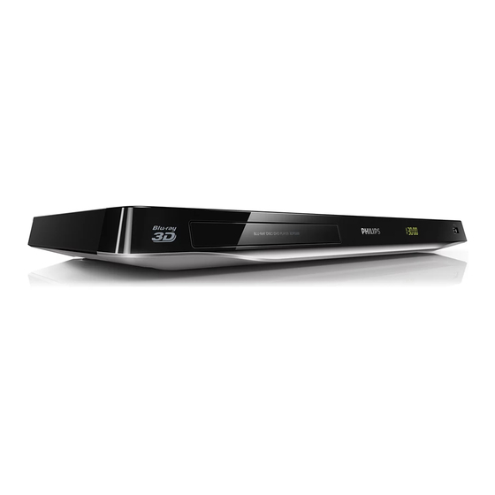
Blu-ray Disc Player
TABLE OF CONTENTS
Location of PCB Boards & version variation & repair scenario matrix..................... 1-1
Production Specifications ...............................................................................................1-2
Remote control ...............................................................................................................1-
Brife guide ......................................................................................................................1-
Safety Instruction, Warning & Notes...............................................................................1-
Mechanical and Dismantling Instructions .......................................................................2-1
Software Version & Upgrades.........................................................................................3-1
Trouble Shooting Chart .....................................................................................................-1
Set Block & Wiring Diagrams ............................................................................5-1
Electrical Diagrams and PCB layouts ................................................................6-1
Set Mechanical Exploded view ....................................................................................... -1
Revision List ...................................................................................................................
©
Copyright 2010 Philips Consumer Electronics B.V. Eindhoven, The Netherlands
All rights reserved. No part of this publication may be reproduced, stored in a retrieval system or
transmitted, in any form or by any means, electronic, mechanical, photocopying, or otherwise without
the prior permission of Philips.
Published by Helen-RY 1201 Service Audio Printed in The Netherlands Subject to modification
Version 1.2
Version 1.1
Version 0.0
BDP5500/12/05/51/55/93/98/X78
Page
4
5
10
4
7
-1
8
CLASS 1
LASER PRODUCT
©
313978536011
GB
GB

Related Manuals for Philips BDP5500/12


Summary of Contents for Philips BDP5500/12
- Page 1 LASER PRODUCT © Copyright 2010 Philips Consumer Electronics B.V. Eindhoven, The Netherlands All rights reserved. No part of this publication may be reproduced, stored in a retrieval system or transmitted, in any form or by any means, electronic, mechanical, photocopying, or otherwise without the prior permission of Philips.
- Page 2 LOCATION OF PCB BOARDS: MAIN BOARD LOADER POWER BOARD FRONT CABINET Version Variation Type/Versions BDP5500 X/78 Features Power supply rating:220-240V ,60Hz Power supply rating:230-240V ,60Hz Power supply rating:110-240V ,50Hz,60Hz Power consumption:20W Repair Scenario Matrix Type/Versions BDP5500 X/78 Board in used Main Board Power Board Front Board...
- Page 3 Main unit media BDP5500/05: USB storage device Power supply rating: AC 230-240V~, 50 Hz File format BDP5500/12/51: Video: .avi, .divx, .mp4, .mkv, .wmv Power supply rating: AC 220-240V~, 50 Hz Audio: .mp3, .wma, .wav BDP5500/55/93/98/X78: Picture: .jpg, .gif, .png Power supply rating: AC 110-240V~, 50 Hz,60 Hz...
- Page 4 Remote Control During play, press the following buttons to control. Button Action Turn on the player, or switch to standby. Access the home menu. Stop play. Press and hold (more than 4 seconds) to open or close the disc compartment. Pause play.
- Page 5 Brife Guide Register your product and get support at www.philips.com/welcome BDP5500 EN User manual HDMI OUT VIDEO VIDEO FOR VOD/BD-LIVE ONL Y HDMI OUT COAXIA O O XIAL A A AL AUDIO LINE OUT UDIO LINE OU...
- Page 6 1 HDMI HDMI VIDEO COAXIAL AUDIO LINE OUT HDMI O 2 VIDEO+AUDIO LINE OUT HDMI VIDEO COAXIAL AUDIO LINE OUT AUDIO LINE OUT IO LINE VIDEO O VIDEO O...
- Page 7 3 COAXIAL HDMI VIDEO COAXIAL AUDIO LINE OUT COAX COAXIA A L IA A L 4 AUDIO LINE OUT HDMI VIDEO COAXIAL AUDIO LINE OUT AUDIO LINE...
- Page 8 SOURCE...
- Page 9 BD/BD 3D DVD/VCD/CD DivX Plus HD/MKV MP3 / JPEG...
- Page 10 Make sure that, • Use only lead-free soldering tin Philips SAC305 with order during repair, you are connected with the same potential as code 0622 149 00106. If lead-free solder paste is required, the mass of the set by a wristband with resistance.
- Page 11 1 - 10 Safety Instructions, Warnings, Notes, and Abbreviation List 2.3.5 Alternative BOM identification Abbreviation List It should be noted that on the European Service website, 0/6/12 SCART switch control signal on A/V “Alternative BOM” is referred to as “Design variant”. board.
- Page 12 Electro Magnetic Interference LORE LOcal REgression approximation EPLD Erasable Programmable Logic Device noise reduction Europe LG.Philips LCD (supplier) EXTernal (source), entering the set by Loudspeaker SCART or by cinches (jacks) LVDS Low Voltage Differential Signalling Fast BLanking: DC signal Mbps...
- Page 13 4.406250 MHz and 4.250000 MHz Sound Intermediate Frequency SMPS Switched Mode Power Supply System on Chip Sync On Green SOPS Self Oscillating Power Supply S/PDIF Sony Philips Digital InterFace SRAM Static RAM Service Reference Protocol Small Signal Board STBY STand-BY SVGA 800x600 (4:3)
- Page 14 Mechanical and Dismantling Instructions Dismantling Instruction Detailed information please refer to the model set. The following guidelines show how to dismantle the player. Step1: Remove 4 screws around the Top Cover, and then remove the Top Cover (Figure 1). Figure 1 Step2: If it is necessary to dismantle Loader or Front Panel, the Front door should be removed first.
- Page 15 Mechanical and Dismantling Instructions Detailed information please refer to the model set. Dismantling Instruction Step3: Dismantling Front Panel, disconnect the connectors (XP5, XP2,XP4)(Figure 3) Then Remove1 PCS Screw away(Figure 3) XP15 XP13 Remove1 PCS Screw right here CN503 Figure 3 Step4: Dismantling Front Panel, need release 2 snaps of Front Panel and 2 snaps of bottom cabinet , then gently pull the Panel out from the set.
- Page 16 Mechanical and Dismantling Instructions Dismantling Instruction Detailed information please refer to the model set. )(Figure 3) aiming in the below figure, and remove 2 screws Step5: Dismantling Loader, disconnect the 3 connectors (XP15 ,XP13,XP6 . (Figure 5) IFI Board, need release 1 snap of WIFI Board , then gently pull the Panel out from the set. (Figure 5 ) :Dismantling Step6 Figure 5...
- Page 17 * Once software updated is complete, this player automatically truns to reboot. C) Update software via USB Flash Drive: 1) Go to www.philips.com/support to check if the latest software version is available for this player. 2) Download the software onto a USB flash drive.
- Page 18 Trouble shooting chart No display on LED, and buttons do not work No display on LED, and buttons do not work Check every supply Check whether the voltage on main board is connction of line is normal(Pin 6 and pin9 is 5v in xs1 on front board) Fix it Check the front board...
- Page 19 Trouble shooting chart No audio output No audio output Check whether the audio Check the U16 power supply signal is right from the (U16:9pin=3.3V) U16:’3pin and12pin R1116 is ok Replace the U16 Check If the R1034,R88 Add these two components is on...
- Page 20 Trouble shooting chart Remote control does not work Remote control does not work Check whether the remote Replace the battery for remote controller’s battery controller exhausted or not. Check the ET3045 power supply ET3045 Check the VCC net on front board (PIN20 )is about 5V Replace ET3045...
- Page 21 Trouble shooting chart Can’t read disc or can’t open the disk door Can’t read disc or can’t open the disk door Check whether Check the connection 4pin cable from the DVD loader running is main board normal Check 45pin 9pin cable from main board Fix the connection the 45pin cable or connection to the loader is...
- Page 22 Trouble shooting chart No video display No Video display Check if L3 is on main board Add L3 Add R617 is 0 ohm Check If R617 is on main board Replace the main board...
- Page 23 Trouble shooting chart Can not connect to network Can not connect to network Check if LFE8634(U12) Fix U12 in mainboard is on In mainboard Check Fix all the resistors R580,R581,R582,R583,R 584 is on in main board Check if the P4 is ok Change P4 Or not...
- Page 24 Trouble shooting chart Can not connect to WIFI Can not connect to WIFI Check (pin1) Check the FB18 is fixed on voltage is 3.3v the mainboard Check the order of wifi Check the connection wire:yellow\white\red from wifi board to to yellow \white\red mainboard Change the wifi wire Change the wifi module...
- Page 25 BDP5500/12/05/51/55/98/93/X78 Block Diagram: coaxial HDMI NET PORT USB port CVBS SMSC8701 DRV632 CVBS SPDIF LOADER :L9828B FLASH OPU:SANYO 415 1Gb DDR3 MT8580 1333M 8pin 1Gb DDR3 1333M TPIC_LOADER- VCC_D(STANDBY :0V,NORMAL:+5V) TPIC_LOADER+ OPEN_K(NOMAL:+5V ) MGND TRAYIN POWER_K(NOMAL:+5V ) VCC(+5V) 1.1V G5693 G556B 1.5V...
- Page 26 Front Board Circuit Diagram: IRM_12mm IRM_12mm IR CIRCUIT VCC_D 2.2K 2.2K R315 R315 R311 R311 R310 R310 R309 R309 4.7K 4.7K 4.7K 4.7K 4.7K 4.7K U301 U301 ET6202 ET6202 GRID[1:7] 1uF/16V/Y5V 1uF/16V/Y5V GRID1 GRID1 47pF/50V/NP0 47pF/50V/NP0 0.1uF/50V/X7R 0.1uF/50V/X7R VSDA R312 R312 GRID1 GRID2...
- Page 27 Power Board circuit diagram: L501 L501 680uH 680uH CY503 CY503 470PF/250Vac 470PF/250Vac C501 C501 D501 D501 D503 D503 R505A R505A R505B R505B R505C R505C R505D R505D 103/1KV 103/1KV CY504 CY504 470PF/250Vac 470PF/250Vac R506 R506 RL207 RL207 RL207 RL207 CE501 CE501 CE502 CE502 CE503...
- Page 28 Main Board circuit diagram for BDP5500/05/51/55/93/98/X78:Power Source GND1 GND1 VCC1 VCC1 1.2V A1.2V 0.1uF/16V/Y5V 0.1uF/16V/Y5V Close to DC-DC 10/2A 10/2A +12V 10uF/10V/Y5V 10uF/10V/Y5V 0.1uF/16V/Y5V 0.1uF/16V/Y5V 10/2A 10/2A FB713 FB713 10/2A 10/2A N24V 2K/1% 2K/1% 2.2uH/3A 2.2uH/3A 6PIN/2.5mm 6PIN/2.5mm C334 C334 N24V_P N24V_P 22uF/6.3V/Y5V...
- Page 29 Main Board circuit diagram BDP5500/05/51/55/93/98/X78:DDR PART 1 U101 U101 1.5V A_DQ1 A_RA0 U102 U102 A_DQ6 A_RA1 U100A U100A 3.3V AG14 A_DQ0 A_DQ0 A_RA2 A_DQ19 A_RA0_2R A_DQS1 TP102 TP102 DDRVCCIO1 RDQ0 AF15 A_DQ1 A_DQ7 A_RA3 A_DQ23 A_RA1_2R A_DQS1# DDRVCCIO1 RDQ1 NC721 NC721 AVDD33_MEMPLL AH14...
- Page 30 Main Board circuit diagram BDP5500/05/51/55/93/98/X78:DDR PART 2 1.2V U100B U100B B_DQ0 DVCC12_K RDQ0_B B_DQ1 DVCC12_K RDQ1_B B_DQ2 B_DQS1 DVCC12_K RDQ2_B 1.2V B_DQ3 B_DQS1# TP201 TP201 DVCC12_K RDQ3_B B_DQ4 U201 U201 TP202 TP202 DVCC12_K RDQ4_B B_DQ5 B_DQS0 DVCC12_K RDQ5_B B_DQ6 B_DQ3 B_RA0 B_DQS0# TP203...
- Page 31 Main Board circuit diagram BDP5500/05/51/55/93/98/X78:ETHERNET_USB_SD CARD 3.3V 3.3V_STBY [amute] GPIO0 USB_OC1# GPIO 0 Normal mode GPIO1 USB_EN1# 3.3V VCC3IO GPIO6 USB_OC2# 1 ICE mode Hardware Trap GPIO7 USB_EN2# R542 R542 R533 R533 R549 R549 R551 R551 R553 R553 R579 R579 R544 R544 [aosdata0, aolrck]...
- Page 32 Main Board circuit diagram BDP5500/05/51/55/93/98/X78:FLASH_IR_VFD BDP7700 VFD USE R1402 BDP5500 LED USE R1403 3.3V_STBY NC723 NC723 U100D U100D 3.3V AE19 AG25 NAND Flash VFD/IR Port DVCC33_IO_STB GPIO8 DVCC33_IO_STB GPIO8 AMUTE1 AE20 AC24 GPIO27 DVCC33_IO_STB GPIO27 NC/33 NC/33 POWER_K AG21 NFD7_R C503 C503 C504...
- Page 33 Main Board circuit diagram BDP5500/05/51/55/93/98/X78:CVBS_AUDIO_OK DVIO U100H U100H 3.3V TP16 TP16 VOUTCLK JTAG PORT VOUTCLK TP17 TP17 VOUTHSYNC VOUTHSYNC 3.3V TP18 TP18 VOUTVSYNC VOUTVSYNC R416 R416 R417 R417 R418 R418 R419 R419 TP19 TP19 VOUTD15 VOUTD15 8PIN/1.0mm 8PIN/1.0mm TP20 TP20 VOUTD14 VOUTD7 TRST_...
- Page 34 Main Board circuit diagram BDP5500/05/51/55/93/98/X78:HDMI 3.3V NC715 NC715 AVDD33_VDAC_X HDMI TX Port 0 Differential Signal ! C303 C303 C304 C304 No Through Hole ! 0.1uF/16V/Y5V 0.1uF/16V/Y5V 100 ohm - Impedance 3.3V U100C U100C TX2+ F_TX2+ NC714 NC714 AVDD33_VDAC_BG AVDD33_VDAC_X TX2- F_TX2- AVDD33_VDAC_X TX1+...
- Page 35 6-10 6-10 Main Board circuit diagram BDP5500/05/51/55/93/98/X78:SERVO_FE V14REF FE RS232 Port C702 C702 3.3V 2.2uF/10V/Y5V 2.2uF/10V/Y5V A1.2V U100F U100F AVDD12_1 NC735 NC735 URXD AVDD12_1 C701 C701 FVREF AVDD12_2 UTXD FVREF AVDD12_2 0.1uF/16V/Y5V 0.1uF/16V/Y5V HAVC NC734 NC734 VHAVC HAVC C703 C703 C704 C704 C705...
- Page 36 6-11 6-11 Main Board circuit diagram BDP5500/05/51/55/93/98/X78:MOTOR_DRIVER MOTOR DRIVER TI2050G4 MVCC_T TPIC_TR+ TPIC_TR+ M12V_T TPIC_TR- TPIC_TR- TPIC_A+ TPIC_TL- TPIC_TL- SLED1_P P5V_2 TPIC_A- TPIC_CO_B- TPIC_TL+ SLED1_N STP2_N TPIC_TL+ TPIC_CO_B+ C757 C757 R1359 R1359 TPIC_FR- P12V_3 STP2_P TPIC_FR- TPIC_B+ TPIC_CO_A- C758 C758 R1357 R1357 TPIC_FR+...
- Page 37 6-12 6-12 Front Board Print-layout (Bottom side):...
- Page 38 6-13 6-13 Power Board Print-layout (Bottom side):...
- Page 39 6-14 6-14 Main Board Print-layout (Top side):...
- Page 40 6-15 6-15 Main Board Print-layout (Bottom side):...
- Page 41 Exploded view for BDP5500/12/05/51/55/93/98/X78:...
- Page 42 REVISION LIST Version 1.0 * Initial release for BDP5500/12/05/51/55/93/98 Version 1.1 * Initial release for BDP5500X/78...