Table of Contents
Quick Links
Table of Contents

Related Manuals for Panasonic KX-TG4011LAT


Summary of Contents for Panasonic KX-TG4011LAT
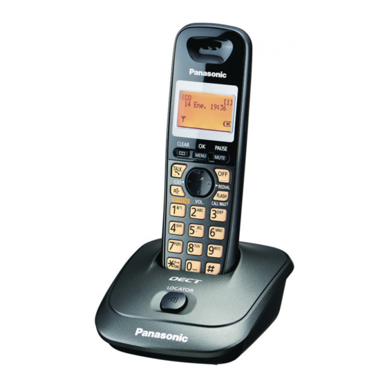
- Page 1 ORDER NO. KM41006120CE Telephone Equipment KX-TG4011LAT Model No. KX-TG4012LAT KX-TG4013LAT KX-TGA403LAT Expandable Digital Cordless Phone T: Black Metallic Version (for Latin America) © Panasonic System Networks Co., Ltd. 2010 Unauthorized copying and distribution is a violation of law.
- Page 2 KX-TG4011LAT/KX-TG4012LAT/KX-TG4013LAT/KX-TGA403LAT...
-
Page 3: Table Of Contents
KX-TG4011LAT/KX-TG4012LAT/KX-TG4013LAT/KX-TGA403LAT TABLE OF CONTENTS PAGE PAGE 1 Safety Precautions----------------------------------------------- 4 16.5. Replacement Parts List--------------------------------- 76 1.1. For Service Technicians --------------------------------- 4 2 Warning -------------------------------------------------------------- 4 2.1. Battery Caution--------------------------------------------- 4 2.2. About Lead Free Solder (PbF: Pb free)-------------- 4 2.3. Discarding of P. C. Board-------------------------------- 5... -
Page 4: Safety Precautions
KX-TG4011LAT/KX-TG4012LAT/KX-TG4013LAT/KX-TGA403LAT 1 Safety Precautions 1.1. For Service Technicians • Repair service shall be provided in accordance with repair technology information such as service manual so as to prevent fires, injury or electric shock, which can be caused by improper repair work. -
Page 5: Discarding Of P. C. Board
KX-TG4011LAT/KX-TG4012LAT/KX-TG4013LAT/KX-TGA403LAT 2.2.1. Suggested PbF Solder There are several types of PbF solder available commercially. While this product is manufactured using Tin, Silver, and Copper (Sn+Ag+Cu), you can also use Tin and Copper (Sn+Cu), or Tin, Zinc, and Bismuth (Sn+Zn+Bi). Please check the manufacturer's specific instructions for the melting points of their products and any precautions for using their product with other materials. -
Page 6: Specifications
KX-TG4011LAT/KX-TG4012LAT/KX-TG4013LAT/KX-TGA403LAT 3 Specifications Note: • Design and specifications are subject to change without notice. Note for Service: • Operation range: Up to 300 m outdoors, Up to 50 m indoors, depending on the condition. • Analog telephone connection: Telephone Line... -
Page 7: Technical Descriptions
KX-TG4011LAT/KX-TG4012LAT/KX-TG4013LAT/KX-TGA403LAT 4 Technical Descriptions 4.1. US-DECT Description The frequency range of 1.91 GHz-1.93 GHz is used. Transmitting and receiving carrier between base unit and handset is same frequency. Refer to Frequency Table (P.53). 4.1.1. TDD Frame Format 4.1.2. TDMA system This system is the cycles of 10 ms, and has 6 duplex paths, but maximum duplex communication path is 5 because of dummy bearer use. - Page 8 KX-TG4011LAT/KX-TG4012LAT/KX-TG4013LAT/KX-TGA403LAT 4.1.3. Signal Flowchart in the Radio Parts Reception A voice signal from TEL line is encoded to digital data "TXDATA" by BBIC (IC501) in a base unit. Then TXDATA goes to RF PART and it's modulated to 1.9 GHz. The RF signal is amplified and fed to a selected antenna.
-
Page 9: Block Diagram (Base Unit_Main)
KX-TG4011LAT/KX-TG4012LAT/KX-TG4013LAT/KX-TGA403LAT 4.2. Block Diagram (Base Unit_Main) -
Page 10: Block Diagram (Base Unit_Rf Part)
KX-TG4011LAT/KX-TG4012LAT/KX-TG4013LAT/KX-TGA403LAT 4.3. Block Diagram (Base Unit_RF Part) ANT2 ANT2 ANT1 DA801 TXON RXON ANT1 KX-TG4011/4012/4013 BLOCK DIAGRAM (Base Unit_RF Part) -
Page 11: Circuit Operation (Base Unit)
KX-TG4011LAT/KX-TG4012LAT/KX-TG4013LAT/KX-TGA403LAT 4.4. Circuit Operation (Base Unit) General Description: (BBIC, EERROM) is a digital speech/signal processing system that implements all the functions of speech compression and memory management required in a digital telephone. The BBIC system is fully controlled by a host processor. The host processor provides activation and control of all that functions as follows. - Page 12 KX-TG4011LAT/KX-TG4012LAT/KX-TG4013LAT/KX-TGA403LAT 4.4.3. Power Supply Circuit/Reset Circuit The power supply voltage from AC adaptor is converted to VBAT (3.0V) in IC302. And +3.0V for peripherals and analog part is insulated from VBAT by Doubler of BBIC. Circuit Operation:...
- Page 13 KX-TG4011LAT/KX-TG4012LAT/KX-TG4013LAT/KX-TGA403LAT 4.4.3.1. Charge Circuit The voltage from the AC adaptor is supplied to the charge circuits.
- Page 14 KX-TG4011LAT/KX-TG4012LAT/KX-TG4013LAT/KX-TGA403LAT 4.4.4. Telephone Line Interface Telephone Line Interface Circuit: Function • Bell signal detection • ON/OFF hook and pulse dial circuit • Side tone circuit Bell signal detection and OFF HOOK circuit: In the idle mode, Q141 is open to cut the DC loop current and decrease the ring load. When ring voltage appears at the Tip (T) and Ring (R) leads (When the telephone rings), the AC ring voltage is transferred as follows: T →...
- Page 15 KX-TG4011LAT/KX-TG4012LAT/KX-TG4013LAT/KX-TGA403LAT 4.4.5. Parallel Connection Detect Circuit/Auto Disconnect Circuit Function: In order to disable call waiting and stutter tone functions when using telephones connected in parallel, it is necessary to have a circuit that judges whether a telephone connected in parallel is in use or not. This circuit determines whether the telephone connected in parallel is on hook or off hook by detecting changes in the T/R voltage.
- Page 16 KX-TG4011LAT/KX-TG4012LAT/KX-TG4013LAT/KX-TGA403LAT 4.4.6. Calling Line Identification (Caller ID) Function: Caller ID The caller ID is a chargeable ID which the user of a telephone circuit obtains by entering a contract with the telephone company to utilize a caller ID service. For this reason, the operation of this circuit assumes that a caller ID service contract has been entered for the circuit being used.
- Page 17 KX-TG4011LAT/KX-TG4012LAT/KX-TG4013LAT/KX-TGA403LAT Call Waiting Caller ID Calling Identity Delivery on Call Waiting (CIDCW) is a CLASS service that allows a customer, while off-hook on an existing call, to receive information about a calling party on a waited call. The transmission of the calling information takes place almost immediately after the customer is alerted to the new call so he/she can use this information to decide whether to take the new call.
-
Page 18: Block Diagram (Handset)
KX-TG4011LAT/KX-TG4012LAT/KX-TG4013LAT/KX-TGA403LAT 4.5. Block Diagram (Handset) ANT1 EEPROM 10.368 MHz BATTERY CHG_DET CHG_CTL Power_adj IC801 VDD_PADRV RESET PSEL C144 CHARGE TXON RXON RF_RXn RF_RXp BATTERY 1.8V RF PART CP_VOUT2 BATTERY LD0_CTRL BATTERY BBIC VDDPA MICp 1.8V MICn Receiver VDD2 LSRp VDD1... -
Page 19: Block Diagram (Handset_Rf Part)
KX-TG4011LAT/KX-TG4012LAT/KX-TG4013LAT/KX-TGA403LAT 4.6. Block Diagram (Handset_RF Part) TXON DA801 RXON RF_RXn RF_RXp KX-TGA403 BLOCK DIAGRAM (Handset_RF Part) -
Page 20: Circuit Operation (Handset)
KX-TG4011LAT/KX-TG4012LAT/KX-TG4013LAT/KX-TGA403LAT 4.7. Circuit Operation (Handset) 4.7.1. Outline Handset consists of the following ICs as shown in Block Diagram (Handset) (P.18). • DECT BBIC (Base Band IC): IC1 - All data signals (forming/analyzing ACK or CMD signal) - All interfaces (ex: Key, Detector Circuit, Charge, DC/DC Converter, EEPROM, LCD, RF Power Amp.) - Page 21 KX-TG4011LAT/KX-TG4012LAT/KX-TG4013LAT/KX-TGA403LAT 4.7.3. Charge Circuit Circuit Operation: When charging the handset on the Base Unit, the charge current is as follows; DC+(6.5 V) → F301 → R371 → R372 →CHARGE+(Base) → CHARGE+(Handset) → Q4 → D7→ F1 → BATTERY+... Battery... BATTERY- → R45 → GND → CHARGE-(Handset)→ CHARGE-(Base) → GND → DC-(GND) In this way, the BBIC on Handset detects the fact that the battery is charged.
-
Page 22: Circuit Operation (Charger Unit)
KX-TG4011LAT/KX-TG4012LAT/KX-TG4013LAT/KX-TGA403LAT 4.8. Circuit Operation (Charger Unit) Charge control is executed at handset side so that the operation when using charger is also controlled by handset. Refer to Circuit Operation (Handset) (P.20) The route for this is as follows: DC+pin of J1(+) → F1 → R1 → CHARGE+pad → Handset → CHARGE-pad → DC-pin of J1(-). -
Page 23: Signal Route
KX-TG4011LAT/KX-TG4012LAT/KX-TG4013LAT/KX-TGA403LAT 4.9. Signal Route RF part signal route... -
Page 24: Location Of Controls And Components
KX-TG4011LAT/KX-TG4012LAT/KX-TG4013LAT/KX-TGA403LAT 5 Location of Controls and Components Refer to the Operating Instructions. Note: You can download and refer to the Operating Instructions (Instruction book) on TSN Server. 6 Installation Instructions Refer to the Operating Instructions. Note: You can download and refer to the Operating Instructions (Instruction book) on TSN Server. -
Page 25: Test Mode
KX-TG4011LAT/KX-TG4012LAT/KX-TG4013LAT/KX-TGA403LAT 8 Test Mode 8.1. Engineering Mode 8.1.1. Base Unit... - Page 26 KX-TG4011LAT/KX-TG4012LAT/KX-TG4013LAT/KX-TGA403LAT Frequently Used Items (Base Unit) ex.) Items Address Default Data New Data Remarks Frequency 00 07 / 00 08 00/01 Use these items in a READ-ONLY mode to confirm the contents. Careless rewriting may 00 02 ~ 00 06 Given value cause serious damage to the computer system.
- Page 27 KX-TG4011LAT/KX-TG4012LAT/KX-TG4013LAT/KX-TGA403LAT 8.1.2. Handset...
- Page 28 KX-TG4011LAT/KX-TG4012LAT/KX-TG4013LAT/KX-TGA403LAT Frequently Used Items (Handset) ex.) Items Address Default Data New Data Possible Adjusted Possible Adjusted Remarks Value MAX (hex) Value MIN (hex) Battery Low 00 11 / 00 12 00 / 00 (*2) Frequency 00 07 / 00 08...
-
Page 29: Service Mode
KX-TG4011LAT/KX-TG4012LAT/KX-TG4013LAT/KX-TGA403LAT 9 Service Mode 9.1. How to Clear User Setting (Handset Only) Handset Press simultaneously until a beep sound is heard. Then single handset is initialized. (The contents of user setting are reset to factory default) *Usage time is not cleared. -
Page 30: Troubleshooting Guide
KX-TG4011LAT/KX-TG4012LAT/KX-TG4013LAT/KX-TGA403LAT 10 Troubleshooting Guide 10.1. Troubleshooting Flowchart Cross Reference: Check Power (P.31) Check Battery Charge (P.32) Check Link (P.33) Check the RF part (P.35) Check Handset Transmission (P.40) Check Handset Reception (P.40) Check Caller ID (P.40) - Page 31 KX-TG4011LAT/KX-TG4012LAT/KX-TG4013LAT/KX-TGA403LAT 10.1.1. Check Power 10.1.1.1. Base Unit Cross Reference: Note: Power Supply Circuit/Reset Circuit (P.12) BBIC is IC501. (*1) Refer to Specifications (P.6) for part number and supply voltage of AC adaptor. (*2) Refer to Circuit Board (Base Unit_Main) (P.67).
- Page 32 KX-TG4011LAT/KX-TG4012LAT/KX-TG4013LAT/KX-TGA403LAT 10.1.2. Check Battery Charge 10.1.2.1. Base Unit Cross Reference: Charge Circuit (P.13) 10.1.2.2. Handset Cross Reference: Check Power (P.31) Charge Circuit (P.21) 10.1.2.3. Charger Unit Cross Reference: Charge Circuit (P.21)
- Page 33 KX-TG4011LAT/KX-TG4012LAT/KX-TG4013LAT/KX-TGA403LAT 10.1.3. Check Link 10.1.3.1. Base Unit Cross Reference: Power Supply Circuit/Reset Circuit (P.12) Check the RF part (P.35) Note: *1 How to adjust +3.0V: Execute the command "VDA" Refer to Things to Do after Replacing IC or X'tal (P.51) for Base Unit.
- Page 34 KX-TG4011LAT/KX-TG4012LAT/KX-TG4013LAT/KX-TGA403LAT 10.1.3.2. Handset Cross Reference: Power Supply Circuit/Reset Circuit (P.20) Check the RF part (P.35) Note: *1 How to adjust the frequency of X1: To see the frequency, execute the command “SFR“, then check the TP_CKM (IC1-46pin). To adjust frequency, send command “SFR “...
- Page 35 KX-TG4011LAT/KX-TG4012LAT/KX-TG4013LAT/KX-TGA403LAT 10.1.4. Check the RF part 10.1.4.1. Finding out the Defective part After All the Checkings or Repairing 1. Re-register the checked handset to the checked base unit, and Regular HS to Regular BU. Note: (*1) HS: Handset (*2) BU: Base Unit...
- Page 36 KX-TG4011LAT/KX-TG4012LAT/KX-TG4013LAT/KX-TGA403LAT 10.1.4.2. RF Check Flowchart Each item (1 ~ 6) of RF Check Flowchart corresponds to Check Table for RF part (P.37). Please refer to the each item. Note: (*1) Refer to Check Link (P.33).
- Page 37 KX-TG4011LAT/KX-TG4012LAT/KX-TG4013LAT/KX-TGA403LAT 10.1.4.3. Check Table for RF part Item BU (Base Unit) Check HS (Handset) Check Link Confirmation Normal 1. Register Regular HS to BU (to be 1. Register HS (to be checked) to Regular checked). HS, BU Mode [Normal Mode] 2.
- Page 38 KX-TG4011LAT/KX-TG4012LAT/KX-TG4013LAT/KX-TGA403LAT 10.1.4.4. TEST RANGE Check Circuit block which range is defective can be found by the following check. Item BU (Base Unit) Check HS (Handset) Check Range Confirmation TX TEST 1. Register Regular HS to BU (to be checked). 1. Register HS (to be checked) to Regular BU.
- Page 39 KX-TG4011LAT/KX-TG4012LAT/KX-TG4013LAT/KX-TGA403LAT 10.1.5. Registering a Handset to the Base Unit 10.1.6. Deregistering a Handset 10.1.7. Deregistering All Handsets by the Base Unit...
- Page 40 KX-TG4011LAT/KX-TG4012LAT/KX-TG4013LAT/KX-TGA403LAT 10.1.8. Check Handset Transmission Cross Reference: Signal Route (P.23) 10.1.9. Check Handset Reception Cross Reference: Signal Route (P.23) Note: When checking the RF part, Refer to Check the RF part (P.35). 10.1.10. Check Caller ID Cross Reference: Telephone Line Interface (P.14) Calling Line Identification (Caller ID) (P.16)
-
Page 41: Disassembly And Assembly Instructions
KX-TG4011LAT/KX-TG4012LAT/KX-TG4013LAT/KX-TGA403LAT 11 Disassembly and Assembly Instructions 11.1. Disassembly Instructions 11.1.1. Base Unit... - Page 42 KX-TG4011LAT/KX-TG4012LAT/KX-TG4013LAT/KX-TGA403LAT 11.1.2. Handset...
- Page 43 KX-TG4011LAT/KX-TG4012LAT/KX-TG4013LAT/KX-TGA403LAT 11.1.3. Charger Unit...
-
Page 44: How To Replace The Handset Lcd
KX-TG4011LAT/KX-TG4012LAT/KX-TG4013LAT/KX-TGA403LAT 11.2. How to Replace the Handset LCD Note: The illustrations are simplified in this page. They may differ from the actual product. -
Page 45: Measurements And Adjustments
KX-TG4011LAT/KX-TG4012LAT/KX-TG4013LAT/KX-TGA403LAT 12 Measurements and Adjustments This chapter explains the measuring equipment, the JIG connection, and the PC setting method necessary for the measurement in Troubleshooting Guide (P.30) 12.1. Equipment Required • Digital multi-meter (DMM): it must be able to measure voltage and current. - Page 46 KX-TG4011LAT/KX-TG4012LAT/KX-TG4013LAT/KX-TGA403LAT 12.2.2. Connections (Handset) Connect the DC Power or Battery to BATT+ and BATT-. Connect the JIG cable GND (black) to GND. Connect the JIG cable UTX (yellow) to UTX and URX (red) to URX. Note: *: COM port names may vary depending on what your PC calls it.
- Page 47 KX-TG4011LAT/KX-TG4012LAT/KX-TG4013LAT/KX-TGA403LAT 12.2.3. How to install Batch file into P.C. Note: • “*****” varies depending on the country or models. 12.2.4. Commands See the table below for frequently used commands. Command name Function Example rdeeprom Read the data of EEPROM Type “rdeeprom 00 00 FF”, and the data from address “00 00”...
-
Page 48: Adjustment Standard (Base Unit)
KX-TG4011LAT/KX-TG4012LAT/KX-TG4013LAT/KX-TGA403LAT 12.3. Adjustment Standard (Base Unit) When connecting the simulator equipment for checking, please refer to below. 12.3.1. Bottom View Note: (*1) is referred to No.2 of Check Check Table for RF part (P.37) (*2) is referred to Power Supply Circuit/Reset Circuit (P.12) -
Page 49: Adjustment Standard (Charger Unit)
KX-TG4011LAT/KX-TG4012LAT/KX-TG4013LAT/KX-TGA403LAT 12.4. Adjustment Standard (Charger Unit) When connecting the simulator equipment for checking, please refer to below. 12.4.1. Bottom View Digital Volt Meter /2 W DC POWER DC 6.5 V... -
Page 50: Adjustment Standard (Handset)
KX-TG4011LAT/KX-TG4012LAT/KX-TG4013LAT/KX-TGA403LAT 12.5. Adjustment Standard (Handset) When connecting the simulator equipment for checking, please refer to below. 12.5.1. Component View KX-TGA650XX KX-TGA651XX PNLB1734Y KX-TGA250XX KX-TGA251XX KX-TGA403XX TP_ANT1 TGA650XX TGA651XX C152 C175 R578 TGA250XX TGA251XX TGA403XX C106 C200 C201 R231 C104 C107... -
Page 51: Things To Do After Replacing Ic Or X'tal
KX-TG4011LAT/KX-TG4012LAT/KX-TG4013LAT/KX-TGA403LAT 12.6. Things to Do after Replacing IC or X'tal If repairing or replacing EEPROM and X'tal, it is necessary to download the required data such as Programming data or adjustment data, etc. in memory. The set doesn't operate if it is not executed. - Page 52 KX-TG4011LAT/KX-TG4012LAT/KX-TG4013LAT/KX-TGA403LAT 12.6.1.2. Handset First, operate the PC setting according to The Setting Method of JIG(P.45). Then download the appropriate data according to the following procedures. Items How to download/Required adjustment EEPROM (IC3) Adjusted parameter data is 1) Default batch file: Execute the command “default.bat”.
-
Page 53: Frequency Table
KX-TG4011LAT/KX-TG4012LAT/KX-TG4013LAT/KX-TGA403LAT 12.7. Frequency Table Ch. (hex) TX/RX Frequency (MHz) Channel 0 1928.448 Channel 1 1926.720 Channel 2 1924.992 Channel 3 1923.264 Channel 4 1921.536... -
Page 54: Miscellaneous
KX-TG4011LAT/KX-TG4012LAT/KX-TG4013LAT/KX-TGA403LAT 13 Miscellaneous 13.1. How to Replace the Flat Package IC Even if you do not have the special tools (for example, a spot heater) to remove the Flat IC, with some solder (large amount), a soldering iron and a cutter knife, you can easily remove the ICs that have more than 100 pins. - Page 55 KX-TG4011LAT/KX-TG4012LAT/KX-TG4013LAT/KX-TGA403LAT 13.1.3. How to Install the IC 1. Temporarily fix the FLAT PACKAGE IC, soldering the two marked pins. *Check the accuracy of the IC setting with the corresponding soldering foil. 2. Apply flux to all pins of the FLAT PACKAGE IC.
-
Page 56: How To Replace The Shield Case
KX-TG4011LAT/KX-TG4012LAT/KX-TG4013LAT/KX-TGA403LAT 13.2. How to Replace the Shield Case 13.2.1. Preparation • PbF (: Pb free) Solder • Soldering Iron Tip Temperature of 700°F ± 20°F (370°C ± 10°C) Note: We recommend a 30 to 40 Watt soldering iron. An expert may be able to use a 60 to 80 Watt iron where someone with less experience could overheat and damage the PCB foil. - Page 57 KX-TG4011LAT/KX-TG4012LAT/KX-TG4013LAT/KX-TGA403LAT 13.2.4. How to Install the Shield Case Note: • If you don’t have special tools (ex. Hot air disordering tool), conduct the following operations. • Shield case’s No. : PNMC1013Z 1. Put the shield case. 2. Solder the surroundings.
-
Page 58: How To Replace The Llp
KX-TG4011LAT/KX-TG4012LAT/KX-TG4013LAT/KX-TGA403LAT 13.3. How to Replace the LLP (Leadless Leadframe Package) IC Note: This description is only applied on the model with Shield case. 13.3.1. Preparation • PbF (: Pb free) Solder • Soldering Iron Tip Temperature of 700 °F ± 20 °F (370 °C ± 10 °C) Note: We recommend a 30 to 40 Watt soldering iron. - Page 59 KX-TG4011LAT/KX-TG4012LAT/KX-TG4013LAT/KX-TGA403LAT 13.3.4. How to Install the IC 1. Place the solder a little on the land where the radiation GND pad on IC bottom is to be attached. 2. Place the solder a little on the land where IC pins are to be attached, then place the IC.
-
Page 60: Terminal Guide Of The Ics, Transistors And Diodes
KX-TG4011LAT/KX-TG4012LAT/KX-TG4013LAT/KX-TGA403LAT 13.4. Terminal Guide of the ICs, Transistors and Diodes 13.4.1. Base Unit 13.4.2. Handset... -
Page 61: Schematic Diagram
KX-TG4011LAT/KX-TG4012LAT/KX-TG4013LAT/KX-TGA403LAT 14 Schematic Diagram 14.1. For Schematic Diagram 14.1.1. Base Unit (Schematic Diagram (Base Unit_Main)) 14.1.1.1. Acoustic Testing Mode Notes: 1. DC voltage measurements are taken with voltmeter from the negative voltage line. 2. The schematic diagrams may be modified at any time with the development of new technology. -
Page 62: Schematic Diagram (Base Unit_Main)
KX-TG4011LAT/KX-TG4012LAT/KX-TG4013LAT/KX-TGA403LAT 14.2. Schematic Diagram (Base Unit_Main) ANT2 R807 C892 RXON ANT2 C822 C827 W 0.15mm W 0.2mm L 20mm 3rd layer 1st layer C894 C826 2.2p W 0.2mm L 10mm 1st layer C820 1.5p ANT1 DA802 DA801 C805 C895 L809 C812 2.7p... - Page 63 KX-TG4011LAT/KX-TG4012LAT/KX-TG4013LAT/KX-TGA403LAT +3.0V Q143 Q141 REFERENCE R160 1XX : TEL LINE 3XX : POWER, CHARGE 4XX : MIC, SP Q161 5XX : BBIC R141 6XX : FLASH, EEPROM, KEY, LCD 7XX : FOR DK 100k 8XX : RF C165 NC C163 NC...
-
Page 64: Schematic Diagram (Handset_Main)
KX-TG4011LAT/KX-TG4012LAT/KX-TG4013LAT/KX-TGA403LAT 14.3. Schematic Diagram (Handset_Main) C harge C urrent BATTERY BATT+ 5.6n C340 C341 C342 C1CP1 R406 J39p +1.8V 6.3V R407 BATTERY 330u (MAX500mA) +1.8V BATTERY R401 1.8V 1.8V BATT- D400 R330 R400 Q400 C400 C331 J56p 6.3V K2.2u R331... - Page 65 KX-TG4011LAT/KX-TG4012LAT/KX-TG4013LAT/KX-TGA403LAT R807 W 0.15mm RXON L 20+/-2mm 3rd layer C827 L801 TP_ANT1 *C826 RX_RF C803 RF_RXn 1.5p DA801 BATTERY RF_RXp W 0.125mm L 7.6mm Gap 0.125mm W 0.15mm CP+3.0V W 0.15mm 1st layer L 5.0mm L 5.0mm 1st layer 1st layer...
-
Page 66: Schematic Diagram (Charger Unit)
KX-TG4011LAT/KX-TG4012LAT/KX-TG4013LAT/KX-TGA403LAT 14.4. Schematic Diagram (Charger Unit) R1 12 SCHEMATIC DIAGRAM (Charger Unit) -
Page 67: Printed Circuit Board
KX-TG4011LAT/KX-TG4012LAT/KX-TG4013LAT/KX-TGA403LAT 15 Printed Circuit Board 15.1. Circuit Board (Base Unit_Main) 15.1.1. Component View D142 C115 D143 L361 R162 C142 C168 for JIG R122 R167 R165 C126 R163 C167 C184 R181 C186 C512 C475 C473 C513 C472 C120 C123 C124 C525... - Page 68 KX-TG4011LAT/KX-TG4012LAT/KX-TG4013LAT/KX-TGA403LAT 15.1.2. Bottom View KX-TG4011/4012/4013 CIRCUIT BOARD (Base Unit_Main (Bottom View))
-
Page 69: Circuit Board (Handset_Main)
KX-TG4011LAT/KX-TG4012LAT/KX-TG4013LAT/KX-TGA403LAT 15.2. Circuit Board (Handset_Main) 15.2.1. Component View KX-TGA650XX KX-TGA651XX PNLB1734Y KX-TGA250XX KX-TGA251XX KX-TGA403XX TP_ANT1 RCV+ RCV- TGA650XX TGA651XX C152 C175 R578 TGA250XX TGA251XX TGA403XX C106 C200 R231 C201 C104 C107 C105 C103 C206 C203 R236 C863 C864 C814 C811... - Page 70 KX-TG4011LAT/KX-TG4012LAT/KX-TG4013LAT/KX-TGA403LAT 15.2.2. Bottom View LED12 PNLB1734Y KX-TGA650XX KX-TGA651XX KX-TGA250XX KX-TGA251XX KX-TGA403XX TGA650XX TGA651XX CN51 TGA250XX TGA251XX TGA403XX SOFT_A SOFT_B SOFT_C TALK LEFT RIGHT LED8 LED6 DOWN KX-TGA403 CIRCUIT BOARD (Handset_Main (Bottom View))
-
Page 71: Circuit Board (Charger Unit)
KX-TG4011LAT/KX-TG4012LAT/KX-TG4013LAT/KX-TGA403LAT 15.3. Circuit Board (Charger Unit) 15.3.1. Component View CIRCUIT BOARD (Charger unit (Component View)) 15.3.2. Bottom View TP4 (GND) CIRCUIT BOARD (Charger unit (Bottom View)) -
Page 72: Exploded View And Replacement Parts List
KX-TG4011LAT/KX-TG4012LAT/KX-TG4013LAT/KX-TGA403LAT 16 Exploded View and Replacement Parts List 16.1. Cabinet and Electrical Parts (Base Unit) 7(*1) 7(*1) PCB1 Ref.No. Figure 2.6 8 mm Note: (*1) The SPACERs (No.7) are cut from the excess parts of SPACER (No.108) of Cabinet and Electrical Parts (Handset) -
Page 73: Cabinet And Electrical Parts (Handset)
(*1) This cable is fixed by welding. Refer to How to Replace the Handset LCD (P.44). (*2) The rechargeable Ni-MH battery HHR-4DPA or HHR-4MRT is available through sales route of Panasonic. (*3) Attach the SPACER (No. 119) to the exact location described above. -
Page 74: Cabinet And Electrical Parts (Charger Unit)
KX-TG4011LAT/KX-TG4012LAT/KX-TG4013LAT/KX-TGA403LAT 16.3. Cabinet and Electrical Parts (Charger Unit) 200-1 PCB200 200-3 200-2 200-4 Ref.No. Figure 2 8 mm... -
Page 75: Accessories
KX-TG4011LAT/KX-TG4012LAT/KX-TG4013LAT/KX-TGA403LAT 16.4. Accessories... - Page 76 KX-TG4011LAT/KX-TG4012LAT/KX-TG4013LAT/KX-TGA403LAT 16.5. Replacement Parts List 16.5.1.2. Main P.C. Board Parts Note: 1. RTL (Retention Time Limited) (*1) When replacing IC611 or X501, make the adjustment Note: using PNZZTG4011LA Refer to How to download the data The “RTL” marking indicates that its Retention Time is (P.51) of Things to Do after Replacing IC or X'tal.
- Page 77 KX-TG4011LAT/KX-TG4012LAT/KX-TG4013LAT/KX-TGA403LAT Safety Ref. Part No. Part Name & Description Remarks Safety Ref. Part No. Part Name & Description Remarks R372 ERJ1TYJ5R6U C806 F1G1H2R7A480 2.7p R501 ERJ3GEYJ100 C810 F1G1H2R4A480 2.4p R502 ERJ2GEJ330 C811 F1G1H100A723 10p R505 ERJ2GEJ222 2.2k C812 F1G1HR90A480 0.9p...
- Page 78 KX-TG4011LAT/KX-TG4012LAT/KX-TG4013LAT/KX-TGA403LAT Safety Ref. Part No. Part Name & Description Remarks Safety Ref. Part No. Part Name & Description Remarks PNWIGA403LAR IC (EEPROM) (*2) R331 ERJ2GEJ273X IC801 C1CB00001842 IC R332 ERJ2GEJ273X (TRANSISTORS) R801 ERJ2GEJ122 1.2k B1ADGE000004 TRANSISTOR(SI) R802 ERJ2GEJ101 B1ADGE000004 TRANSISTOR(SI)
- Page 79 KX-TG4011LAT/KX-TG4012LAT/KX-TG4013LAT/KX-TGA403LAT Safety Ref. Part No. Part Name & Description Remarks Safety Ref. Part No. Part Name & Description Remarks E101 L5DYBYY00012 LIQUID CRYSTAL DISPLAY PQZZ430PIR TIP OF SOLDERING IRON (*3) (*2) E102 PNHR1247Z TRANSPARENT PLATE, LCD PMMA-HB PQZZ430PRB RUBBER OF SOLDERING IRON...