
Related Manuals for Asus AAEON ASDM-L-CFS


Summary of Contents for Asus AAEON ASDM-L-CFS
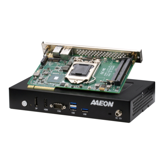
- Page 1 ASDM-L-CFS Smart Display Module User’s Manual 1 Last Updated: April 23, 2020...
- Page 2 Copyright Notice This document is copyrighted, 2020. All rights are reserved. The original manufacturer reserves the right to make improvements to the products described in this manual at any time without notice. No part of this manual may be reproduced, copied, translated, or transmitted in any form or by any means without the prior written permission of the original manufacturer.
- Page 3 Acknowledgement All other products’ name or trademarks are properties of their respective owners. Microsoft Windows is a registered trademark of Microsoft Corp. ⚫ Intel®, Pentium®, Celeron®, and Xeon® are registered trademarks of Intel ⚫ Corporation Core™, Atom™ are trademarks of Intel Corporation ⚫...
- Page 4 Packing List Before setting up your product, please make sure the following items have been shipped: Item Quantity ASDM-L-CFS ⚫ If any of these items are missing or damaged, please contact your distributor or sales representative immediately. Preface...
- Page 5 About this Document This User’s Manual contains all the essential information, such as detailed descriptions and explanations on the product’s hardware and software features (if any), its specifications, dimensions, jumper/connector settings/definitions, and driver installation instructions (if any), to facilitate users in setting up their product. Users may refer to the product page at AAEON.com for the latest version of this document.
- Page 6 Safety Precautions Please read the following safety instructions carefully. It is advised that you keep this manual for future references All cautions and warnings on the device should be noted. Make sure the power source matches the power rating of the device. Position the power cord so that people cannot step on it.
- Page 7 If any of the following situations arises, please the contact our service personnel: Damaged power cord or plug Liquid intrusion to the device iii. Exposure to moisture Device is not working as expected or in a manner as described in this manual The device is dropped or damaged Any obvious signs of damage displayed on the device...
- Page 8 FCC Statement This device complies with Part 15 FCC Rules. Operation is subject to the following two conditions: (1) this device may not cause harmful interference, and (2) this device must accept any interference received including interference that may cause undesired operation.
- Page 9 China RoHS Requirements (CN) 产品中有毒有害物质或元素名称及含量 AAEON Main Board/ Daughter Board/ Backplane 有毒有害物质或元素 部件名称 铅 汞 镉 六价铬 多溴联苯 多溴二苯醚 (Pb) (Hg) (Cd) (Cr(VI)) (PBB) (PBDE) 印刷电路板 × ○ ○ ○ ○ ○ 及其电子组件 外部信号 × ○ ○ ○ ○ ○ 连接器及线材...
- Page 10 China RoHS Requirement (EN) Poisonous or Hazardous Substances or Elements in Products AAEON Main Board/ Daughter Board/ Backplane Poisonous or Hazardous Substances or Elements Hexavalent Polybrominated Polybrominated Component Lead Mercury Cadmium Chromium Biphenyls Diphenyl Ethers (Pb) (Hg) (Cd) (Cr(VI)) (PBB) (PBDE) PCB &...
-
Page 11: Table Of Contents
Table of Contents Chapter 1 - Product Specifications..................1 Specifications ......................2 Chapter 2 – Hardware Information ..................4 Dimensions ....................... 5 2.1.1 Module dimensions ..................5 2.1.2 With Thermal Option and I/O Bracket ............ 6 Jumpers and Connectors ..................7 List of Jumpers ...................... - Page 12 Setup submenu: Advanced ................. 29 3.4.1 Trusted Computing ..................30 3.4.2 CPU Configuration ..................32 3.4.3 SATA Configuration ................... 34 3.4.4 Hardware Monitor ..................35 3.4.4.1 Smart Fan Mode Configuration ............. 36 3.4.5 SIO Configuration ..................38 3.4.5.1 Serial Port 1 Configuration .............. 39 3.4.6 SerialIo Configuration ................
- Page 13 List of Mating Connectors and Cables .............. 69 Preface XIII...
-
Page 14: Chapter 1 - Product Specifications
Chapter 1 Chapter 1 - Product Specifications Preface... -
Page 15: Specifications
Specifications System Form Factor Intel SDM-L Module Generation Intel® Core™, Pentium®, and Celeron® processors (Coffee Lake S, Coffee Lake Refresh) TDP up to 35W CPU Frequency Up to 4.0 GHz Chipset Intel® Chipsets H310/ Q370 Memory Type DDR4 2666 SO-DIMM x 2 (non-ECC) Max. - Page 16 System Operating Humidity 0% ~ 90% relative humidity, non-condensing MTBF (Hours) — Certification CE/FCC Class A Display Controller Intel® UHD Graphics 630/620/610 Video Output HDMI 2.0 x 1 (through Edge connector) DP1.2 x 1 (through Edge connector) Audio Through HDMI, DP by edge connector Intel®...
-
Page 17: Chapter 2 - Hardware Information
Chapter 2 Chapter 2 – Hardware Information... -
Page 18: Dimensions
Dimensions 2.1.1 Module dimensions Chapter 2 – Hardware Information... -
Page 19: With Thermal Option And I/O Bracket
2.1.2 With Thermal Option and I/O Bracket Chapter 2 – Hardware Information... -
Page 20: Jumpers And Connectors
Jumpers and Connectors Chapter 2 – Hardware Information... -
Page 21: List Of Jumpers
List of Jumpers The ASDM-L-CFS features a number of jumpers allowing for manual configuration of the system to suit the needs of the user. Label Function Clear CMOS Jumper 2.3.1 Clear CMOS Jumper (JP1) 1 2 3 Normal (Default) Clear CMOS Chapter 2 –... -
Page 22: List Of Connectors
List of Connectors The ASDM-L-CFS features a number of connectors and switches allowing for configuration and connection with external devices such as hard disk drives or a keyboard. Label Function CPU FAN Dual USB 3.0 Ports Battery LAN (RJ-45) Port LPC/SM BUS Port M.2 Key-E Slot (2230) M.2 Key-B Slot (2242) -
Page 23: Cpu Fan (Cn1)
2.4.1 CPU FAN (CN1) Pin Name Signal Type Signal Level FAN_POWER +12V FAN_TAC FAN_CTL 2.4.2 Dual USB 3.0 Ports (CN2) Pin Name Signal Type Signal Level +5VSB USB_D- DIFF Chapter 2 – Hardware Information... -
Page 24: Battery (Cn3)
Pin Name Signal Type Signal Level USB_D+ DIFF USB_SSRX− DIFF USB_SSRX+ DIFF USB_SSTX− DIFF USB_SSTX+ DIFF +5VSB USB_D- DIFF USB_D+ DIFF USB_SSRX− DIFF USB_SSRX+ DIFF USB_SSTX− DIFF USB_SSTX+ DIFF 2.4.3 Battery (CN3) Pin Name Signal Type Signal Level +3.3V 3.3V Chapter 2 –... -
Page 25: Lan (Rj45) Port (Cn4)
2.4.4 LAN (RJ45) Port (CN4) Pin Name Signal Type Signal Level MDI0+ DIFF MDI0- DIFF MDI1+ DIFF MDI2+ DIFF MDI2- DIFF MDI1- DIFF MDI3+ DIFF MDI3- DIFF Chapter 2 – Hardware Information... -
Page 26: Lpc/Sm Bus Port (Cn5)
2.4.5 LPC/SM BUS Port (CN5) Pin Name Signal Type Signal Level LAD0 +3.3V LAD1 +3.3V LAD2 +3.3V LAD3 +3.3V +3.3V +3.3V LFRAME# LRESET# +3.3V LCLK HWRST PWRBTN Chapter 2 – Hardware Information... -
Page 27: Key-E Slot (2230) (Cn6)
2.4.6 M.2 Key-E Slot (2230) (CN6) Pin Name Signal Type Signal Level +3.3VSB +3.3V USB_D+ DIFF +3.3VSB +3.3V USB_D- DIFF Chapter 2 – Hardware Information... - Page 28 Pin Name Signal Type Signal Level PCIE_TX+ DIFF PCIE_TX- DIFF PCIE_RX+ DIFF PCIE_RX- DIFF PCIE_REF_CLK+ DIFF PCIE_REF_CLK- DIFF PCIE_RST# +3.3V PCIE_CLK_REQ# +3.3V W_DISABLE2# +3.3V PCIE_WAKE# +3.3V W_DISABLE1# +3.3V Chapter 2 – Hardware Information...
-
Page 29: Key-B Slot (2242) (Cn7)
Pin Name Signal Type Signal Level +3.3VSB +3.3V +3.3VSB +3.3V +3.3VSB +3.3V 2.4.7 M.2 Key-B Slot (2242) (CN7) Pin Name Signal Type Signal Level +3.3V +3.3V +3.3V +3.3V USB_D+ DIFF W_DISABLE Chapter 2 – Hardware Information... - Page 30 Pin Name Signal Type Signal Level USB_D- DIFF SSD_LED# PERN1/USB3.0-RX- DIFF PERN1/USB3.0-RX+ DIFF PERN1/USB3.0-TX- DIFF PERN1/USB3.0-TX+ DIFF DEVSLP PERN0/SATA-B+ DIFF PERN0/SATA-B- DIFF Chapter 2 – Hardware Information...
- Page 31 Pin Name Signal Type Signal Level PETN0/SATA-A- DIFF PETN0/SATA-A+ DIFF PERST# CLKREQ# REFCLKN DIFF PEWAKE# REFCLKP DIFF +3.3V +3.3V Chapter 2 – Hardware Information...
-
Page 32: Spi Debug Port (Cn8)
Pin Name Signal Type Signal Level +3.3V +3.3V +3.3V +3.3V 2.4.8 SPI Debug Port (CN8) Pin Name Signal Type Signal Level SPI_MISO SPI_CLK +3.3VSB +3.3V SPI_MOSI SPI_CS 2.4.9 DDR SO-DIMM Slot (DIMM1/DIMM2) DDR SO-DIMM Slots follow standard specifications. Chapter 2 – Hardware Information... -
Page 33: Sdm Gold Finger (Gf1)
2.3.8 SDM Gold Finger (GF1) Pin Name Signal Type Signal Level +12V +12V +12V +12V +12V +12V PWRGD# +3.3V SLP_S4 +3.3V SDM_DET# I2C0_SDA +3.3V I2C0_SCL +3.3V GSPI_CLK +1.8V GSPI_CS0# +1.8V PCIE_TX+ DIFF PCIE_TX- DIFF PCIE_RX+ DIFF PCIE_RX- DIFF PCIE_REF_CLK+ DIFF PCIE_REF_CLK- DIFF PCIE_WAKE#... - Page 34 PCIE_RST# +3.3V HDMI_CLK_N DIFF HDMI_CLK_P DIFF HDMI_D0_N DIFF HDMI_D0_P DIFF HDMI_D1_N DIFF HDMI_D1_P DIFF HDMI_D2_N DIFF HDMI_D2_P DIFF HDMI_SDA +3.3V HDMI_SCL +3.3V HDMI_HPD +12V +12V +12V +12V +3VSB +3.3V Chapter 2 – Hardware Information...
- Page 35 PWRBTN# RESET# SYSFAN# I2C1_SDA +3.3V I2C1_SCL +3.3V GSPI_MOSI +1.8V GSPI_MISO +1.8V UART_TXD +3.3V UART_RXD +3.3V USB_SSTX+ DIFF USB_SSTX− DIFF USB_SSRX+ DIFF USB_SSRX− DIFF USB_D+ DIFF USB_D- DIFF USB_OC# DP3- DIFF DP3+ DIFF DP2- DIFF DP2+ DIFF Chapter 2 – Hardware Information...
- Page 36 DP1- DIFF DP1+ DIFF DP0- DIFF DP0+ DIFF DP_AUX- DIFF DP_AUX+ DIFF DP_HPD Chapter 2 – Hardware Information...
-
Page 37: Function Block
Function Block Electrical Specifications for I/O Ports Reference Signal Output CPU FAN +12V +12V/0.5A USB 3.0 Ports +5VSB +5V/1A (per channel) LPC/SM BUS Port +3.3V +3.3V/0.5A M.2 Key-E (2230) +3.3VSB +3.3V/2A M.2 Key-B (2242) +3.3VSB +3.3V/2.5A Chapter 2 – Hardware Information... -
Page 38: Chapter 3 - Ami Bios Setup
Chapter 3 Chapter 3 - AMI BIOS Setup... -
Page 39: System Test And Initialization
System Test and Initialization The ASDM-L-CFS module uses certain routines to perform testing and initialization during the boot up sequence. If an error, fatal or non-fatal, is encountered, the module will output a few short beeps or display an error message. The module can usually continue the boot up sequence with non-fatal errors. -
Page 40: Ami Bios Setup
AMI BIOS Setup The AMI BIOS ROM has a pre-installed Setup program that allows users to modify basic system configurations. These configurations are stored in the battery-backed CMOS RAM and BIOS NVRAM so the information is retained when power is turned off. To enter BIOS Setup, press... -
Page 41: Setup Submenu: Main
Setup submenu: Main Chapter 3 – AMI BIOS Setup... -
Page 42: Setup Submenu: Advanced
Setup submenu: Advanced Chapter 3 – AMI BIOS Setup... -
Page 43: Trusted Computing
3.4.1 Trusted Computing Options Summary Security Device Support Disable Enable Optimal Default, Failsafe Default Enables or Disables BIOS support for security device. O.S. will not show Security Device. TCG EFI protocol and INT1A interface will not be available. SHA-1 PCR Bank Disable Enable Optimal Default, Failsafe Default... - Page 44 Options Summary Platform Hierarchy Disabled Enabled Optimal Default, Failsafe Default Enable or disable Platform Hierarchy Storage Hierarchy Disabled Enabled Optimal Default, Failsafe Default Enable or Disable Storage Hierarchy Endorsement Hierarchy Disabled Enabled Optimal Default, Failsafe Default Enable or Disable Endorsement Hierarchy TPM2.0 UEFI Spec TCG_1_2 Version...
-
Page 45: Cpu Configuration
3.4.2 CPU Configuration Options Summary Hyper-Threading Disabled Enabled Optimal Default, Failsafe Default Enabled or Disabled Hyper-Threading Technology Active Processor Cores Optimal Default, Failsafe Default Number of cores to enable in each processor package. Intel (VMX) Virtualization Disabled Technology Enabled Optimal Default, Failsafe Default When enabled, a VMM can utilize the additional hardware capabilities provided by Vanderpool Technology. - Page 46 Options Summary Intel(R) SpeedStep(tm) Disabled Enabled Optimal Default, Failsafe Default Allows more than two frequency ranges to be supported. Turbo Mode Disabled Enabled Optimal Default, Failsafe Default Enable/Disable processor Turbo Mode (requires Intel Speed Step or Intel Speed Shift to be available and enabled).
-
Page 47: Sata Configuration
3.4.3 SATA Configuration Options Summary SATA Controller(s) Disabled Enabled Optimal Default, Failsafe Default Enable/Disable SATA Device. M.2(SATA) Disabled Enabled Optimal Default, Failsafe Default Enable or Disable SATA Port Chapter 3 – AMI BIOS Setup... -
Page 48: Hardware Monitor
3.4.4 Hardware Monitor Options Summary Smart Fan Disable Enable Optimal Default, Failsafe Default Enables or Disables Smart Fan. Chapter 3 – AMI BIOS Setup... -
Page 49: Smart Fan Mode Configuration
3.4.4.1 Smart Fan Mode Configuration Options Summary CPU Smart Fan Full Mode Optimal Default, Failsafe Default Control Manual Mode by PWM Auto Mode by PWM PWM signal Non-inverting Inverting Optimal Default, Failsafe Default Select output PWM of inverting or non-inverting signal Monitor Thermal THERMAL_SRC1(T1) Optimal Default, Failsafe Default... - Page 50 Options Summary Start of PWM Optimal Default, Failsafe Default Start PWM Slope (PWM) 1 (PWM) Optimal Default, Failsafe Default Slope (PWM) Chapter 3 – AMI BIOS Setup...
-
Page 51: Sio Configuration
3.4.5 SIO Configuration Chapter 3 – AMI BIOS Setup... -
Page 52: Serial Port 1 Configuration
3.4.5.1 Serial Port 1 Configuration Options Summary Use This Device Disable Enable Optimal Default, Failsafe Default Enable or Disable this Logical Device. Possible: Use Automatic Settings Optimal Default, Failsafe Default IO=3F8h; IRQ=4 IO=2C8h; IRQ=11 Allows user to change Device's Resource settings. New settings will be reflected on This Setup Page after System restarts. -
Page 53: Serialio Configuration
3.4.6 SerialIo Configuration Options Summary SPI0 Controller Disable Optimal Default, Failsafe Default Enable Enables/Disables SerialIo Controller If given device is Function 0 PSF disabling is skipped. PSF default will remain and device PCI CFG Space will still be visible. This is needed to allow PCI enumerator access functions above 0 in a multifunction device. -
Page 54: Power Management
3.4.7 Power Management Options Summary Power Mode ATX Type Optimal Default, Failsafe Default AT Type Select system power mode State After G3 S0 State Optimal Default, Failsafe Default S5 State Last State Specify what state to go to when power is re-applied after a power failure (G3 state). RTC wake system Disable Optimal Default, Failsafe Default... -
Page 55: Setup Submenu: Chipset
Setup submenu: Chipset Chapter 3 – AMI BIOS Setup... -
Page 56: System Agent (Sa) Configuration
3.5.1 System Agent (SA) Configuration Chapter 3 – AMI BIOS Setup... -
Page 57: Pch-Io Configuration
3.5.2 PCH-IO Configuration Options Summary HD Audio Disabled Enabled Optimal Default, Failsafe Default Control Detection of the HD-Audio device. Disabled = HDA will be unconditionally disabled Enabled = HDA will be unconditionally enabled. PCH Lan Controller Disabled Enabled Optimal Default, Failsafe Default Enable/Disable onboard NIC Chapter 3 –... -
Page 58: Setup Submenu: Security
Setup submenu: Security Change User/Administrator Password You can set an Administrator Password or User Password. An Administrator Password must be set before you can set a User Password. The password will be required during boot up, or when the user enters the Setup utility. A User Password does not provide access to many of the features in the Setup utility. -
Page 59: Secure Boot
3.6.1 Secure Boot Options Summary Secure Boot Disabled Optimal Default, Failsafe Default Enabled Secure Boot feature is Active if Secure Boot is Enabled, Platform Key(PK) is enrolled and the System is in User mode. The mode change requires platform reset Secure Boot Mode Custom Optimal Default, Failsafe Default... -
Page 60: Key Management
3.6.1.1 Key Management Options Summary Factory Key Provision Disabled Optimal Default, Failsafe Default Enabled Secure Boot feature is Active if Secure Boot is Enabled, Platform Key (PK) is enrolled and the System is in User mode. The mode change requires platform reset Restore Factory Keys Force System to User Mode. - Page 61 Options Summary Remove 'UEFI CA' from DB Device Guard ready system must not list 'Microsoft UEFI CA' Certificate in Authorized Signature database (db) Restore DB defaults Restore DB variable to factory defaults Platform Key(PK) Details Export Update Delete Key Exchange Keys Details Export Update...
-
Page 62: Setup Submenu: Boot
Setup submenu: Boot Options Summary Quiet Boot Disabled Enabled Optimal Default, Failsafe Default Enable/Disable showing boot logo. LAN UEFI Pxe Driver Disabled Optimal Default, Failsafe Default Enabled Enabled/Disable LAN UEFI PXE Driver Chapter 3 – AMI BIOS Setup... -
Page 63: Bbs Priorities
3.7.1 BBS Priorities Chapter 3 – AMI BIOS Setup... -
Page 64: Setup Submenu: Save & Exit
Setup submenu: Save & Exit Chapter 3 – AMI BIOS Setup... -
Page 65: Chapter 4 - Drivers Installation
Chapter 4 Chapter 4 – Drivers Installation... -
Page 66: Driver Download And Installation
Driver Download and Installation Drivers for the ASDM-L-CFS can be downloaded from the product page on the AAEON website by following this link: https://www.aaeon.com/en/p/smart-display-modules-asdm-l-cfs Download the driver(s) you need and follow the steps below to install them. Before beginning installation, use the following chart to determine if your operating system (OS) is compatible with the drivers AAEON provides for the ASDM-L-CFS. - Page 67 Step 2 – Install Graphics Drivers (Windows 10 only) Open the Step 2 - Graphic folder Run the igxpin.exe file in the folder Follow the instructions Drivers will be installed automatically Step 3 – Install Network Drivers Open the Step 3 - Network folder and select your OS Run the ProWinx64.exe file in the folder Follow the instructions Drivers will be installed automatically...
-
Page 68: Appendix A - Watchdog Timer Programming
Appendix A Appendix A - Watchdog Timer Programming... -
Page 69: Watchdog Timer Initial Program
Watchdog Timer Initial Program Table 1 : Embedded BRAM relative register table Default Value Note Index 0x284(Note1) BRAM Index Register Data 0x285(Note2) BRAM Data Register Logical Device Number 0xA8(Note3) Watch dog Logical Device Number Function and Device Number 0x00(Note4) Watch dog Function/Device Number Table 2 : Watchdog relative register table Option Register BitNum... - Page 70 ************************************************************************************ // Embedded BRAM relative definition (Please reference to Table 1) #define byte EcBRAMIndex //This parameter is represented from Note1 #define byte EcBRAMData //This parameter is represented from Note2 #define byte BRAMLDNReg //This parameter is represented from Note3 #define byte BRAMFnDataReg //This parameter is represented from Note4 #define void EcBRAMWriteByte(byte Offset, byte Value);...
- Page 71 ************************************************************************************ VOID Main(){ // Procedure : AaeonWDTConfig // (byte)Timer : Time of WDT timer.(0x00~0xFF) // (boolean)Unit : Select time unit(0: second, 1: minute). AaeonWDTConfig(); // Procedure : AaeonWDTEnable // This procudure will enable the WDT counting. AaeonWDTEnable(); ************************************************************************************ Appendix A – Watchdog Timer Programming...
- Page 72 ************************************************************************************ // Procedure : AaeonWDTEnable VOID AaeonWDTEnable (){ WDTEnableDisable(1); // Procedure : AaeonWDTConfig VOID AaeonWDTConfig (){ // Disable WDT counting WDTEnableDisable(0); // WDT relative parameter setting WDTParameterSetting(); VOID WDTEnableDisable(byte Value){ ECBRAMWriteByte(TimerReg , Value); VOID WDTParameterSetting(){ By te TempByte; // Watchdog Timer counter setting ECBRAMWriteByte(TimerReg , TimerVal);...
- Page 73 ************************************************************************************ VOID ECBRAMWriteByte(byte OPReg, byte OPBit, byte Value){ IOWriteByte(EcBRAMIndex, 0x10); IOWriteByte(EcBRAMData, BRAMLDNReg); IOWriteByte(EcBRAMIndex, 0x11); IOWriteByte(EcBRAMData, BRAMFnDataReg); IOWriteByte(EcBRAMIndex, 0x13 + OPReg); IOWriteByte(EcBRAMData, Value); IOWriteByte(EcBRAMIndex, 0x12); IOWriteByte(EcBRAMData, 0x30); //Write start Byte ECBRAMReadByte(byte OPReg){ IOWriteByte(EcBRAMIndex, 0x10); IOWriteByte(EcBRAMData, BRAMLDNReg); IOWriteByte(EcBRAMIndex, 0x11); IOWriteByte(EcBRAMData, BRAMFnDataReg); IOWriteByte(EcBRAMIndex, 0x12); IOWriteByte(EcBRAMData, 0x10);...
-
Page 74: Appendix B - I/O Information
Appendix B Appendix B - I/O Information... -
Page 75: I/O Address Map
I/O Address Map Appendix B – I/O Information... - Page 76 Appendix B – I/O Information...
-
Page 77: Memory Address Map
Memory Address Map Appendix B – I/O Information... -
Page 78: Irq Mapping Chart
IRQ Mapping Chart Appendix B – I/O Information... - Page 79 Appendix B – I/O Information...
- Page 80 Appendix B – I/O Information...
-
Page 81: Appendix C - Mating Connectors And Cables
Appendix C Appendix C – Mating Connectors and Cables... - Page 82 List of Mating Connectors and Cables The table notes mating connectors and available cables. Connector Function Mating Connector Available Cable P/N Label Cable Vendor Model No External Molex 51021-0200 Battery Cable 1750113019 Connector Appendix C – Mating Connectors and Cables...