Table of Contents
SERVICE MANUAL
Ver. 1.1 2014.04
The service manual of the mechanism deck, used in
this model, has been issued in a separate volume.
Please refer to the service manual of the MG-101
series for the mechanism deck information.
• The tuner and CD sections have no adjustments.
(MEX-GS610BT only)
FOR THE CUSTOMERS IN THE USA. NOT
APPLICABLE IN CANADA, INCLUDING IN THE
PROVINCE OF QUEBEC.
POUR LES CLIENTS AUX ÉTATS-UNIS. NON
APPLICABLE AU CANADA, Y COMPRIS LA
PROVINCE DE QUÉBEC.
(MEX-GS610BT only)
AUDIO POWER SPECIFICATIONS
CEA2006 Standard
Power Output: 17 Watts RMS × 4 at 4
Ohms < 1% THD+N
SN Ratio: 80 dBA
(reference: 1 Watt into 4 Ohms)
Tuner section
(
)
MEX-GS610BT
FM
Tuning range: 87.5 – 107.9 MHz
Antenna (aerial) terminal:
External antenna (aerial) connector
Intermediate frequency: 25 kHz
Usable sensitivity: 8 dBf
Selectivity: 75 dB at 400 kHz
Signal-to-noise ratio: 80 dB (stereo)
Separation: 50 dB at 1 kHz
Frequency response: 20 – 15,000 Hz
9-893-930-02
Sony Corporation
2014D33-1
©
2014.04
Published by Sony Techno Create Corporation
MEX-GS610BE/GS610BT/
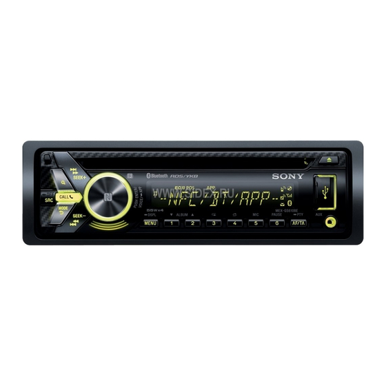
Photo: MEX-GS610BT
Model Name Using Similar Mechanism
Mechanism Type
Optical Pick-up Name
SPECIFICATIONS
(MEX-N6050BT)
AM
Tuning range: 530 – 1,710 kHz
FM
Antenna (aerial) terminal:
Tuning range:
External antenna (aerial) connector
Intermediate frequency:
9,115 kHz or 9,125 kHz/5 kHz
Sensitivity: 26 μV
FM tuning step:
(MEX-GS610BE)
Antenna (aerial) terminal:
FM
Tuning range:
Intermediate frequency: 25 kHz
FM1/FM2: 87.5 – 108.0 MHz
Usable sensitivity: 8 dBf
(at 50 kHz step)
Selectivity: 75 dB at 400 kHz
FM3: 65 – 74 MHz (at 30kHz step)
Signal-to-noise ratio: 80 dB (stereo)
Antenna (aerial) terminal:
Separation: 50 dB at 1 kHz
External antenna (aerial) connector
Frequency response: 20 – 15,000 Hz
Intermediate frequency: 25 kHz
AM
Usable sensitivity: 8 dBf
Tuning range:
Selectivity: 75 dB at 400 kHz
Signal-to-noise ratio: 80 dB (stereo)
Separation: 50 dB at 1 kHz
AM tuning step:
Frequency response: 20 – 15,000 Hz
Antenna (aerial) terminal:
MW/LW
Tuning range:
Intermediate frequency:
MW: 531 – 1,602 kHz
LW: 153 – 279 kHz
Antenna (aerial) terminal:
Sensitivity: 26 μV
External antenna (aerial) connector
Intermediate frequency:
9,124.5 kHz or 9,115.5 kHz/4.5 kHz
Sensitivity: MW: 26 μV, LW: 45 μV
CD Player section
Signal-to-noise ratio: 120 dB
Frequency response: 10 – 20,000 Hz
87.5 – 108.0 MHz (at 50 kHz step)
Wow and flutter: Below measurable limit
87.5 – 108.0 MHz (at 100 kHz step)
Corresponding codec: MP3 (.mp3) and WMA (.wma)
87.5 – 107.9 MHz (at 200 kHz step)
USB Player section
50 kHz/100 kHz/200 kHz switchable
Interface: USB (High-speed)
Maximum current: 1 A (front), 2.1 A (rear)
External antenna (aerial) connector
The maximum number of recognizable tracks:
Corresponding codec:
531 – 1,602 kHz (at 9 kHz step)
530 – 1,710 kHz (at 10 kHz step)
9 kHz/10 kHz switchable
External antenna (aerial) connector
9,124.5 kHz or 9,115.5 kHz/4.5 kHz (at 9 kHz step)
9,115 kHz or 9,125 kHz/5 kHz (at 10 kHz step)
N6050BT
US Model
Canadian Model
MEX-GS610BT
E Model
MEX-N6050BT
Russian Model
MEX-GS610BE
CDX-G3000UE/G3000UP/
G3050UV
MG-101CF-188
DAX-25A
10,000
MP3 (.mp3), WMA (.wma) and WAV (.wav)
– Continued on next page –
AUDIO SYSTEM
Table of Contents

Related Manuals for Sony MEX-GS610BE


Summary of Contents for Sony MEX-GS610BE
- Page 1 Sensitivity: 26 μV Frequency response: 20 – 15,000 Hz External antenna (aerial) connector Intermediate frequency: 9,124.5 kHz or 9,115.5 kHz/4.5 kHz Sensitivity: MW: 26 μV, LW: 45 μV AUDIO SYSTEM 9-893-930-02 Sony Corporation 2014D33-1 © 2014.04 Published by Sony Techno Create Corporation...
- Page 2 Bluetooth SIG, Inc. and any HID (Human Interface Device Profile) Mounting dimensions: use of such marks by Sony Corporation is under Approx. 182 mm × 53 mm × 160 mm *1 The actual range will vary depending on factors such license.
-
Page 3: Table Of Contents
MEX-GS610BE/GS610BT/N6050BT SECTION 1 SERVICING NOTES TABLE OF CONTENTS NOTES ON HANDLING THE OPTICAL PICK-UP BLOCK OR BASE UNIT SERVICING NOTES ..........The laser diode in the optical pick-up block may suffer electro- GENERAL static break-down because of the potential difference generated by .............. - Page 4 MEX-GS610BE/GS610BT/N6050BT DESTINATION SETTING METHOD 1-3. Entering the Destination Code When the complete MAIN board or IC502 on the MAIN board is • Method of operation by main unit replaced, the destination setting is necessary. 1. Destination Setting Set destination according to the procedure below.
- Page 5 MEX-GS610BE/GS610BT/N6050BT Ver. 1.1 1-4. Destination Code TEST DISCS Use following TEST DISC (for CD) when this unit confi rms the Model Destination OP5 OP4 OP3 OP2 OP1 OP0 operation and checks it. MEX-GS610BE Russian MEX-GS610BT US, Canadian Part No. Description...
- Page 6 MEX-GS610BE/GS610BT/N6050BT IMPORTANT NOTE OF “INITIALIZING” REPLACING THE LITHIUM BATTERY OF THE REMOTE The purpose of “Bluetooth Initialize” is to initialize the Bluetooth COMMANDER connection history (HF/Audio Streaming). (To delete the device When the battery becomes weak, the range of the information for the devices that you connected to when searching, remote commander becomes shorter.
- Page 7 1. Search for this unit from the Bluetooth device (cellular phone), • Speaker connection (at least Front L/R ch) and confi rm whether this unit (“Sony Car Audio”) is displayed. • DC power supply (12 V) 2. Search for the distance of this unit and the Bluetooth device (cellular phone) about 5 m apart.
- Page 8 MEX-GS610BE/GS610BT/N6050BT BLUETOOTH INFORMATION WRITING METHOD 2. Writing the NFC Tag Data When the complete MAIN board, knob (VOL) (SV) assy or front Write the NFC tag data (Bluetooth information) to the NFC mod- panel (SV) assy is replaced, the writing of Bluetooth information ule in the knob (VOL) (SV) assy.
- Page 9 MEX-GS610BE/GS610BT/N6050BT 5. Input the Bluetooth address (BD_ADDR). 10. Check the operation of connecting with the smartphone by one (Input the Bluetooth address (BD_ADDR) that written on the touch (NFC). BT module label with the keyboard on the smartphone, or Tap “OPERATION CHECK OF THE NFC AFTER...
- Page 10 MEX-GS610BE/GS610BT/N6050BT 16. Tap the “Read” on the screen of the smartphone. 4. Check Method of the NFC Tag Data Check the NFC tag data according to the procedure below. Procedure: 1. Set the unit to the state where the BT module (Ref. No. IC1002 on the MAIN board) can be seen.
- Page 11 MEX-GS610BE/GS610BT/N6050BT 5. The Factor that One Touch Connection is Impossible The four following factors are considered as the factor that one touch connection is impossible. Guess and check the defective factor by each checking result. Note: The four following factors are examples.
- Page 12 MEX-GS610BE/GS610BT/N6050BT AFFIXING OF LABEL (SERIAL NUMBER) When the front panel (SV) (assy) is replaced, it is necessary to affi x the label (serial number). 2 labels (serial number) are included with a new front panel (SV) (assy). Affi x 1 label to the rear side of the front panel (SV) (assy). Affi x the other one to the bottom side of main unit.
- Page 13 MEX-GS610BE/GS610BT/N6050BT • Please cut out along the dotted line and use it. Notice about the serial number change on the back side of Notice about the serial number change on the back side of the front panel: the front panel:...
- Page 14 MEX-GS610BE/GS610BT/N6050BT MEMO...
- Page 15 MEX-GS610BE/GS610BT/N6050BT SERVICE POSITION CD mechanism deck CD mechanism deck insulating sheet insulating sheet stand stand cable flexible flat (27 core) cable flexible flat (27 core) main unit main unit Note: Do not cable flexible flat (27 core) is Note: Do not cable flexible flat (27 core) is damaged by the edge of the chassis.
-
Page 16: General
MEX-GS610BE/GS610BT/N6050BT SECTION 2 This section is extracted GENERAL from instruction manual. (MEX-GS610BT) Equipment used in illustrations (not supplied) Appareils utilisés dans les illustrations (non fournis) Smartphone, iPod/iPhone, USB device Front speaker Subwoofer Power amplifier Rear speaker Téléphone intelligent, iPod/iPhone, Haut-parleur avant... - Page 17 You may not be able to install this unit in some makes Montage de l’appareil dans une temperatures and humidity. of Japanese cars. In such a case, consult your Sony Pour capturer votre voix durant les appels mains voiture japonaise ( ) It is extremely dangerous if the cord becomes dealer.
- Page 18 MEX-GS610BE/GS610BT/N6050BT (MEX-GS610BE) В зависимости от типа автомобиля используйте адаптер (не входит в комлект Використовуйте адаптер (не входить до комплекту постачання), якщо роз’єм антени поставки), если разъем антенны не подходит. не підходить – це залежить від автомобіля. Кабель с разъемами RCA (не входит в комлект поставки) Шнур...
- Page 19 замініть запобіжник. Якщо запобіжник перегорає устройства. В этом случае обратитесь к знову після заміни, причиною цього може бути Зажимы (не входят в комлект поставки) ближайшему дилеру Sony. Затискачі (не входять до комплекту постачання) внутрішня неполадка. У такому разі зверніться до найближчого дилера Sony.
- Page 20 MEX-GS610BE/GS610BT/N6050BT (MEX-N6050BT) Equipment used in illustrations (not supplied) Equipo utilizado en las ilustraciones (no suministrado) Smartphone, iPod/iPhone, USB device Front speaker Subwoofer Power amplifier Rear speaker Teléfono inteligente, iPod/iPhone, Altavoz frontal Altavoz potenciador de graves Amplificador de potencia Altavoz posterior...
- Page 21 Montaje de la unidad en un It is extremely dangerous if the cord becomes of Japanese cars. In such a case, consult your Sony wound around the steering column or gearstick. Be Para capturar la voz durante llamadas con manos automóvil japonés ( )
-
Page 22: Disassembly
MEX-GS610BE/GS610BT/N6050BT SECTION 3 DISASSEMBLY • This set can be disassembled in the order shown below. 3-1. DISASSEMBLY FLOW FRONT PANEL SECTION Note: Illustration of disassembly is omitted. 3-2. MINI FUSE (BLADE TYPE) (10A/32V) (FU1), COVER (Page 22) 3-3. SUB PANEL ASSY (Page 23) 3-4. -
Page 23: Sub Panel Assy
MEX-GS610BE/GS610BT/N6050BT 3-3. SUB PANEL ASSY 2 two claws 3 sub panel assy Note: When installing the sub panel assy, align two ribs and two holes. hole hole 2 two claws 1 two screws (PTT2.6 3-4. CD MECHANISM DECK (MG-101CF-188) Note 1: The service manual of the mechanism deck, used in this model has been issued in a sepa- rate volume. -
Page 24: Connection Cable (Automobile) ( ) (Cnc1)
MEX-GS610BE/GS610BT/N6050BT Ver. 1.1 3-5. CONNECTION CABLE (AUTOMOBILE) ( ) (CNC1) Note 1: REGULATOR board has been deleted in the midway of production. For details, please refer to service manual supplement-1. 5 connection cable (automobile) ( (CNC1) 4 screw (PTT2.6 1 filament... -
Page 25: Main Board
MEX-GS610BE/GS610BT/N6050BT Ver. 1.1 3-6. MAIN BOARD 3-7. ANTENNA BT (BT1) Note 1: When the complete MAIN board is replaced, it is necessary to replace knob (VOL) (SV) assy simultaneously. Also, the destination setting, Bluetooth operation check and Bluetooth information writing is necessary. Refer to “DESTINATION SETTING METHOD” on page 3 lead wire with connector 4, “BLUETOOTH FUNCTION CHECKING METHOD USING A CELLULAR PHONE”... -
Page 26: Diagrams
MEX-GS610BE/GS610BT/N6050BT SECTION 5 DIAGRAMS 5-1. BLOCK DIAGRAM - SERVO/BT/USB Section - CD MECHANISM DECK BLOCK (MG-101CF-188) FL, RL, SUB FPI1 RFRP 27 RFZI DAO3 (F_L-CH) (Page 17 FPI2 DAO2 (F_R-CH) R-CH 16 FNI1 DAO4 (R_L-CH) 15 FNI2 DAO1 (R_R-CH) R-CH... -
Page 27: Block Diagram - Main Section
MEX-GS610BE/GS610BT/N6050BT 5-2. BLOCK DIAGRAM - MAIN Section - INPUT SELECTOR, ELECTRICAL VOLUME IC402 J401 FL, RL, SUB 33 AU_IN_FL AU_OUT_FL FRONT (Page R-CH 31 AU_IN_RL AU_OUT_RL REAR AUDIO OUT R-CH 30 AU_IN_SUB AU_OUT_SL KEY BOARD (2/3) AU_OUT_SR AUX_L 8 AUX_LCH... -
Page 28: Block Diagram - Panel/Power Supply Section
MEX-GS610BE/GS610BT/N6050BT Ver. 1.1 5-3. BLOCK DIAGRAM - PANEL/POWER SUPPLY Section - RESET SYSTEM CONTROLLER IC503 (3/3) (Page RESET SIGNAL 120 RC_IN1 GENERATOR J801 IC501 (REMOTE IN) 81 RC_IN0 KEY_ACK0 +1.2V REGULATOR -COM_1.2V IC001 (Former type) IC805 (New type) KEY BOARD (3/3) - Page 29 MEX-GS610BE/GS610BT/N6050BT THIS NOTE IS COMMON FOR PRINTED WIRING BOARDS AND SCHEMATIC DIAGRAMS. • Waveforms (In addition to this, the necessary note is printed in each block.) – MAIN Board – For Printed Wiring Boards. For Schematic Diagrams. IC705 rk (LRCK_OUT)
-
Page 30: Printed Wiring Boards - Main Section (1/2) (Type11: Gs610Bt Only)
MEX-GS610BE/GS610BT/N6050BT Ver. 1.1 5-4. PRINTED WIRING BOARDS - MAIN Section (1/2) (Type11: GS610BT only) - • : Uses unleaded solder. MAIN BOARD (COMPONENT SIDE) C310 C329 C315 C332 D805 C807 D808 C307 R303 C811 R834 C816 R831 C825 R439 R435... -
Page 31: Printed Wiring Boards - Main Section (2/2) (Type11: Gs610Bt Only)
MEX-GS610BE/GS610BT/N6050BT 5-5. PRINTED WIRING BOARDS - MAIN Section (2/2) (Type11: GS610BT only) - • : Uses unleaded solder. MAIN BOARD (CONDUCTOR SIDE) J401 (FRONT VIEW) CN301 AUDIO OUT J1001 J801 REAR FRONT (REMOTE IN) J001 R302 (ANTENNA IN) CN801 REAR LCH (+) -
Page 32: Printed Wiring Boards - Main Section (1/2) (Type31)
MEX-GS610BE/GS610BT/N6050BT Ver. 1.1 5-6. PRINTED WIRING BOARDS - MAIN Section (1/2) (Type31) - • : Uses unleaded solder. MAIN BOARD (COMPONENT SIDE) (GS610BT) C310 C329 C315 C332 D805 C807 D808 C307 R303 C811 R834 C816 R831 C825 R439 R435 R821... -
Page 33: Printed Wiring Boards - Main Section (2/2) (Type31)
MEX-GS610BE/GS610BT/N6050BT Ver. 1.1 5-7. PRINTED WIRING BOARDS - MAIN Section (2/2) (Type31) - • : Uses unleaded solder. MAIN BOARD (CONDUCTOR SIDE) (GS610BT) J401 (FRONT VIEW) CN301 AUDIO OUT J1001 J801 REAR FRONT (REMOTE IN) (GS610BT/N6050BT) J001 R302 (ANTENNA IN) -
Page 34: Schematic Diagram - Main Section (1/4)
MEX-GS610BE/GS610BT/N6050BT 5-8. SCHEMATIC DIAGRAM - MAIN Section (1/4) - • See page 29 for Waveforms. • See page 38 for IC Block Diagrams. • See page 41 for IC Pin Function Description. MAIN BOARD (1/4) JL725 IC702 IC B/D C745... -
Page 35: Schematic Diagram - Main Section (2/4)
MEX-GS610BE/GS610BT/N6050BT 5-9. SCHEMATIC DIAGRAM - MAIN Section (2/4) - • See page 29 for Waveforms. • See page 38 for IC Block Diagrams. • See page 41 for IC Pin Function Description. J401 MAIN BOARD (2/4) FRONT JL401 AUDIO OUT... -
Page 36: Schematic Diagram - Main Section (3/4)
MEX-GS610BE/GS610BT/N6050BT Ver. 1.1 5-10. SCHEMATIC DIAGRAM - MAIN Section (3/4) - • See page 29 for Waveforms. • See page 38 for IC Block Diagrams. (GS610BT/N6050BT) MAIN BOARD (3/4) REAR RCH (+) CN301 REAR LCH (+) RR_P REAR RCH (–) -
Page 37: Schematic Diagram - Main Section (4/4)
MEX-GS610BE/GS610BT/N6050BT 5-11. SCHEMATIC DIAGRAM - MAIN Section (4/4) - • See page 29 for Waveforms. • See page 38 for IC Block Diagrams. • See page 41 for IC Pin Function Description. MAIN BOARD (4/4) MEC_DSW R680 IC B/D IC501... - Page 38 MEX-GS610BE/GS610BT/N6050BT • IC Block Diagrams – MAIN Board – IC301 PURE5001H-4WX IC402 BD3468FV-E2 FADER FADER BOOST LEVEL OUTC SHIFT SELECTION FADER FADER BOOST LEVEL OUTS SHIFT HIGH SIDE DRIVER A1 1 A2 2 FADER FADER LEVEL OUTR1 SHIFT BOOST BP1 3...
- Page 39 MEX-GS610BE/GS610BT/N6050BT IC803 BD49100RFS-E2 LDO5 ADJ5 1 44 GATE5 (CONTROLLER) INTERNAL REGULATOR EN 2 BU_SW LD4EN 3 43 VIN0 UVLO BU_CONT L_DET ECO 4 42 BCAP ERR1 5 41 VINSW ERR2 6 40 N.C. SDA 7 HSIDE SCL 8 39 HSW2...
- Page 40 MEX-GS610BE/GS610BT/N6050BT IC1300 OZ539IGN-A1-0-TR BST 1 VREF OSCILLATOR LX 2 REFERENCE GENERATOR OVER CURRENT PROTECTION GNDA VIN 3 EN_SYS 4 USBOUT 5 FB_USB 6 SS_SYS ADJUSTMENT GENERATOR CHARGE EN_USB PUMP VIC_USB USBIN OVER-CURRENT ISET_USB LIMIT VOUT_SYS (USBIN) UVLS FAULT PROTECTION –...
- Page 41 MEX-GS610BE/GS610BT/N6050BT • IC Pin Function Description MAIN BOARD IC503 R7S7200022CFP (SYSTEM CONTROLLER) Pin No. Pin Name Description BT_MIC_DET External microphone plug insert detection signal input terminal for the Bluetooth AMP_ATT Amplifi er muting on/off control signal output to the power amplifi er “L”: muting on...
- Page 42 MEX-GS610BE/GS610BT/N6050BT Pin No. Pin Name Description MEC_LIMIT Limit in detection switch input terminal Power supply terminal (+1.18V) (for internal) KEYA_CK0 Key acknowledge signal (wake up signal) input from the rotary commander MEC_LOAD Loading motor drive signal (loading direction) output terminal “H”: motor on...
- Page 43 MEX-GS610BE/GS610BT/N6050BT Pin No. Pin Name Description RC_IN1 Rotary commander shift key input terminal Ground terminal RE_ON Jog dial pulse pull-up signal output terminal PVcc Power supply terminal (+3.3V) (for I/O) MEC_DSW Chucking end detection switch input terminal I2C0_SCL Serial data transfer clock signal output to the electrical volume, regulator and EEPROM...
- Page 44 MEX-GS610BE/GS610BT/N6050BT MAIN BOARD IC705 TC94A99FG-003 (SYCH (RF AMP, DIGITAL SERVO PROCESSOR, AUDIO DSP) Pin No. Pin Name Description LPFO PLL circuit low-pass fi lter amplifi er output terminal PVREF PLL circuit reference voltage (+1.65V) terminal VCOF VCO fi lter terminal...
- Page 45 MEX-GS610BE/GS610BT/N6050BT Pin No. Pin Name Description DVSS5 Ground terminal VDD1-3 Power supply terminal (+1.5V) VSS-2 Ground terminal XVSS3 Ground terminal System clock input terminal (16.9344 MHz) System clock output terminal (16.9344 MHz) XVDD3 Power supply terminal (+3.3V) ADVDD3 Power supply terminal (+3.3V)
- Page 46 MEX-GS610BE/GS610BT/N6050BT MAIN BOARD IC1301 PD720114GA-YEU-A-SAK (USB CONTROLLER) Pin No. Pin Name Description VDD25OUT Internal regulator power supply voltage (+2.5V) output terminal VSSREG Ground terminal (for internal regulator) 3 to 6 LED4 to LED1 LED drive signal output terminal Not used...
-
Page 47: Exploded Views
MEX-GS610BE/GS610BT/N6050BT SECTION 6 EXPLODED VIEWS Note: • -XX and -X mean standardized parts, so • The mechanical parts with no reference • Abbreviation they may have some difference from the number in the exploded views are not sup- CND : Canadian model original one. -
Page 48: Chassis Section
MEX-GS610BE/GS610BT/N6050BT Ver. 1.1 6-2. CHASSIS SECTION Note 1: REGULATOR board has been deleted in the midway of production. For details, please refer to service manual supplement-1. CNC1 not supplied (US, CND) not supplied MAIN board not supplied not supplied not supplied... -
Page 49: Electrical Parts List
MEX-GS610BE/GS610BT/N6050BT SECTION 7 MAIN ELECTRICAL PARTS LIST Note: • Due to standardization, replacements in • CAPACITORS When indicating parts by reference num- the parts list may be different from the uF: μF ber, please include the board name. parts specifi ed in the diagrams or the com- •... - Page 50 MEX-GS610BE/GS610BT/N6050BT MAIN Ref. No. Part No. Description Remark Ref. No. Part No. Description Remark * C421 1-116-738-11 CERAMIC CHIP 1uF 6.3V C553 1-216-833-11 METAL CHIP 1/10W (GS610BT) * C422 1-116-738-11 CERAMIC CHIP 1uF 6.3V C559 1-164-940-11 CERAMIC CHIP 0.0033uF (GS610BT)
- Page 51 MEX-GS610BE/GS610BT/N6050BT MAIN Ref. No. Part No. Description Remark Ref. No. Part No. Description Remark C763 1-164-852-11 CERAMIC CHIP 12PF C839 1-164-878-11 CERAMIC CHIP 150PF C840 1-116-739-11 CERAMIC CHIP 0.47uF C764 1-118-345-11 CERAMIC CHIP 0.01uF C841 1-116-739-11 CERAMIC CHIP 0.47uF C765 1-118-477-11 CERAMIC CHIP 2.2uF...
- Page 52 MEX-GS610BE/GS610BT/N6050BT Ver. 1.1 MAIN Ref. No. Part No. Description Remark Ref. No. Part No. Description Remark C1330 1-116-707-11 CERAMIC CHIP 47uF FB504 1-500-113-22 BEAD, FERRITE (CHIP) (1608) C1331 1-116-737-11 CERAMIC CHIP 1uF FB505 1-400-823-11 EMI FERRITE (SMD) (1005) C1332 1-118-386-11 CERAMIC CHIP 0.1uF...
- Page 53 MEX-GS610BE/GS610BT/N6050BT MAIN Ref. No. Part No. Description Remark Ref. No. Part No. Description Remark L1301 1-481-904-11 INDUCTOR 47uH R319 1-250-515-11 METAL CHIP 6.8K 1/16W L1302 1-414-842-21 INDUCTOR 15nH L1303 1-414-842-21 INDUCTOR 15nH R320 1-216-833-11 METAL CHIP 1/10W L1304 1-414-842-21 INDUCTOR...
- Page 54 MEX-GS610BE/GS610BT/N6050BT MAIN Ref. No. Part No. Description Remark Ref. No. Part No. Description Remark R523 1-218-977-11 METAL CHIP 100K 1/16W R600 1-218-941-81 METAL CHIP 1/16W R601 1-218-941-81 METAL CHIP 1/16W R524 1-218-941-81 METAL CHIP 1/16W R525 1-218-941-81 METAL CHIP 1/16W...
- Page 55 MEX-GS610BE/GS610BT/N6050BT MAIN Ref. No. Part No. Description Remark Ref. No. Part No. Description Remark R666 1-216-296-11 SHORT CHIP R762 1-216-845-11 METAL CHIP 100K 1/10W R680 1-218-941-81 METAL CHIP 1/16W R763 1-218-977-11 METAL CHIP 100K 1/16W R681 1-218-977-11 METAL CHIP 100K...
- Page 56 MEX-GS610BE/GS610BT/N6050BT MAIN REGULATOR Ref. No. Part No. Description Remark Ref. No. Part No. Description Remark R856 1-216-073-91 METAL CHIP 1/10W R1303 1-216-809-11 METAL CHIP 1/10W R857 1-218-973-11 METAL CHIP 1/16W R1304 1-250-654-11 METAL CHIP 1/10W R858 1-218-961-11 METAL CHIP 4.7K...
- Page 57 MEX-GS610BE/GS610BT/N6050BT Ver. 1.1 Ref. No. Part No. Description Remark 1-846-979-11 CONNECTION CABLE, AUTOMOBILE (POWER) (US, CND, E) ************************************************************* ACCESSORIES ************ KEY (FRAME) FITTING FRAME ASSY 1-489-810-42 REMOTE COMMANDER (RM-X231) 4-480-657-12 MANUAL, INSTRUCTION (ENGLISH, FRENCH) (GS610BT) 4-480-657-32 MANUAL, INSTRUCTION (RUSSIAN, UKRAINIAN)
- Page 58 MEX-GS610BE/GS610BT/N6050BT MEMO...
- Page 59 MEX-GS610BE/GS610BT/ N6050BT US Model Canadian Model SERVICE MANUAL MEX-GS610BT E Model MEX-N6050BT Russian Model Ver. 1.1 2014.04 MEX-GS610BE SUPPLEMENT-1 SUPPLEMENT-1 File this supplement with the service manual. Subject: Change of MAIN board (Suffi x-41) Deletion of REGULATOR board The MAIN board has been changed in the midway of production.
- Page 60 MEX-GS610BE/GS610BT/N6050BT 2. DIAGRAMS THIS NOTE IS COMMON FOR PRINTED WIRING BOARDS AND SCHEMATIC DIAGRAMS. (In addition to this, the necessary note is printed in each block.) For Printed Wiring Boards. For Schematic Diagrams. Note: Note: • X : Parts extracted from the component side.
- Page 61 MEX-GS610BE/GS610BT/N6050BT 2-1. PRINTED WIRING BOARD - MAIN Board (Component Side) - • : Uses unleaded solder. MAIN BOARD (COMPONENT SIDE) (GS610BT) C310 C329 C315 C332 D805 C807 D808 C307 R303 C811 R834 C816 R831 C825 R439 C405 R435 R821 C312...
- Page 62 MEX-GS610BE/GS610BT/N6050BT 2-2. PRINTED WIRING BOARD - MAIN Board (Conductor Side) - • : Uses unleaded solder. MAIN BOARD (CONDUCTOR SIDE) (GS610BT) J401 (FRONT VIEW) CN301 AUDIO OUT J1001 J801 REAR FRONT (REMOTE IN) (GS610BT/N6050BT) R302 J001 (ANTENNA IN) CN801 REAR LCH (+)
- Page 63 MEX-GS610BE/GS610BT/N6050BT 2-3. SCHEMATIC DIAGRAM - MAIN Board (1/4) - MAIN BOARD (1/4) JL725 IC702 C745 C771 C749 C767 C764 C770 C766 0.01 0.01 0.0022 C793 JL724 +3.3V REGULATOR FB702 IC702 BU33TD3WG-TR R751 CL702 (3.3) VOUT R714 C736 R728 0.001 (3.3)
- Page 64 MEX-GS610BE/GS610BT/N6050BT 2-4. SCHEMATIC DIAGRAM - MAIN Board (2/4) - J401 MAIN BOARD (2/4) FRONT JL401 AUDIO OUT C416 10 16V R433 JL402 IN_RL R440 4.7uH C410 10 16V R422 R439 IN_RR REAR C409 10 R421 R416 IN_FL R420 C415 L401...
- Page 65 MEX-GS610BE/GS610BT/N6050BT 2-5. SCHEMATIC DIAGRAM - MAIN Board (3/4) - (GS610BT/N6050BT) MAIN BOARD (3/4) REAR RCH (+) CN301 REAR LCH (+) RR_P REAR RCH (–) RL_P REAR LCH (–) RR_N IC301 RR– FRONT RCH (+) RL_N RL– FRONT LCH (+) CN301...
- Page 66 MEX-GS610BE/GS610BT/N6050BT 2-6. SCHEMATIC DIAGRAM - MAIN Board (4/4) - MAIN BOARD (4/4) MEC_DSW R680 IC501 C524 C571 C533 RESET SIGNAL GENERATOR IC501 R574 BU4228F-STR VOUT 4 C528 CT 3 R513 R567 R571 R579 R681 270k R607 100k C502 C564 C519...
- Page 67 MEX-GS610BE/GS610BT/N6050BT MAIN 3. ELECTRICAL PARTS LIST Note: • Due to standardization, replacements in • CAPACITORS When indicating parts by reference num- the parts list may be different from the uF: μF ber, please include the board name. parts specifi ed in the diagrams or the com- •...
- Page 68 MEX-GS610BE/GS610BT/N6050BT MAIN Ref. No. Part No. Description Remark Ref. No. Part No. Description Remark C425 1-116-728-11 CERAMIC CHIP 2.2uF * C567 1-116-738-11 CERAMIC CHIP 1uF 6.3V C441 1-164-866-11 CERAMIC CHIP 47PF C568 1-115-416-11 CERAMIC CHIP 0.001uF C442 1-164-866-11 CERAMIC CHIP 47PF...
- Page 69 MEX-GS610BE/GS610BT/N6050BT MAIN Ref. No. Part No. Description Remark Ref. No. Part No. Description Remark C768 1-118-459-11 CERAMIC CHIP 0.01uF C845 1-114-813-11 CERAMIC CHIP 1uF C769 1-116-728-11 CERAMIC CHIP 2.2uF C846 1-116-716-11 CERAMIC CHIP 10uF C770 1-118-459-11 CERAMIC CHIP 0.01uF C847...
- Page 70 MEX-GS610BE/GS610BT/N6050BT MAIN Ref. No. Part No. Description Remark Ref. No. Part No. Description Remark C1333 1-118-386-11 CERAMIC CHIP 0.1uF FB702 1-469-084-21 INDUCTOR, FERRITE BEAD (1005) C1334 1-118-386-11 CERAMIC CHIP 0.1uF FB703 1-469-084-21 INDUCTOR, FERRITE BEAD (1005) C1336 1-162-923-11 CERAMIC CHIP 47PF...
- Page 71 MEX-GS610BE/GS610BT/N6050BT MAIN Ref. No. Part No. Description Remark Ref. No. Part No. Description Remark < TRANSISTOR > R404 1-208-939-11 METAL CHIP 150K 0.5% 1/16W R406 1-216-864-11 SHORT CHIP Q401 6-552-936-01 TRANSISTOR LTC014EUBFS8TL R407 1-216-296-11 SHORT CHIP Q402 6-552-922-01 TRANSISTOR LTA014EUBFS8TL...
- Page 72 MEX-GS610BE/GS610BT/N6050BT MAIN Ref. No. Part No. Description Remark Ref. No. Part No. Description Remark R529 1-218-977-11 METAL CHIP 100K 1/16W R607 1-218-941-81 METAL CHIP 1/16W R533 1-218-990-81 SHORT CHIP R608 1-218-990-81 SHORT CHIP R534 1-218-957-11 METAL CHIP 2.2K 1/16W R609...
- Page 73 MEX-GS610BE/GS610BT/N6050BT MAIN Ref. No. Part No. Description Remark Ref. No. Part No. Description Remark R702 1-218-990-81 SHORT CHIP R809 1-250-640-11 METAL CHIP 1/10W R703 1-216-864-11 SHORT CHIP * R810 1-250-523-11 METAL CHIP 1/16W R704 1-216-864-11 SHORT CHIP R811 1-218-990-81 SHORT CHIP...
- Page 74 MEX-GS610BE/GS610BT/N6050BT MAIN Ref. No. Part No. Description Remark Ref. No. Part No. Description Remark R863 1-218-990-81 SHORT CHIP R1312 1-216-821-11 METAL CHIP 1/10W R865 1-208-948-11 METAL CHIP 360K 0.5% 1/16W R1313 1-216-864-11 SHORT CHIP R868 1-216-821-11 METAL CHIP 1/10W R1314...
- Page 75 MEX-GS610BE/GS610BT/N6050BT MEMO...
- Page 76 MEX-GS610BE/GS610BT/N6050BT REVISION HISTORY Checking the version allows you to jump to the revised page. Also, clicking the version at the top of the revised page allows you to jump to the next revised page. Ver. Date Description of Revision 2014.01 2014.04...