Table of Contents
Quick Links
MULTIMEDIA AV NAVIGATION RECEIVER
AVIC-X930BT
AVIC-X9310BT
NAVIGATION AV SYSTEM
AVIC-F930BT
This service manual should be used together with the following manual(s):
Model No.
Order No.
CX-3250
CRT4300
For details, refer to "Important Check Points for Good Servicing".
PIONEER CORPORATION
PIONEER ELECTRONICS (USA) INC. P.O. Box 1760, Long Beach, CA 90801-1760, U.S.A.
PIONEER EUROPE NV Haven 1087, Keetberglaan 1, 9120 Melsele, Belgium
PIONEER ELECTRONICS ASIACENTRE PTE. LTD. 253 Alexandra Road, #04-01, Singapore 159936
PIONEER CORPORATION 2011
Mech. Module
LS1
DVD Mech. Module : Circuit Descriptions, Mech. Descriptions, Disassembly
1-1, Shin-ogura, Saiwai-ku, Kawasaki-shi, Kanagawa 212-0031, Japan
AVIC-X930BT/XNUC
/XNUC
/XNAU
Remarks
ORDER NO.
CRT4695
/XNUC
K-ZZZ MAR. 2011 Printed in Japan
Table of Contents

Related Manuals for Pioneer CX-3250


Summary of Contents for Pioneer CX-3250
- Page 1 PIONEER CORPORATION 1-1, Shin-ogura, Saiwai-ku, Kawasaki-shi, Kanagawa 212-0031, Japan PIONEER ELECTRONICS (USA) INC. P.O. Box 1760, Long Beach, CA 90801-1760, U.S.A. PIONEER EUROPE NV Haven 1087, Keetberglaan 1, 9120 Melsele, Belgium PIONEER ELECTRONICS ASIACENTRE PTE. LTD. 253 Alexandra Road, #04-01, Singapore 159936 PIONEER CORPORATION 2011 K-ZZZ MAR.
-
Page 2: Safety Information
SAFETY INFORMATION CAUTION This service manual is intended for qualified service technicians; it is not meant for the casual do-it-yourselfer. Qualified technicians have the necessary test equipment and tools, and have been trained to properly and safely repair complex products such as those covered by this manual. Improperly performed repairs can adversely affect the safety and reliability of the product and may void the warranty. - Page 3 Laser diode characteristics Wave length: DVD:660 nm to 670 nm CD:780 nm to 800 nm Focus lens on Maximum output: CD:6.26 mW(Emitting period :9 sec.) DVD:1.27 mW (Emitting period : unlimited) Additional Laser Caution Transistors Q1103 and Q1104 in PCB drive the laser diodes for DVD and CD respectively.
- Page 4 [Important Check Points for Good Servicing] In this manual, procedures that must be performed during repairs are marked with the below symbol. Please be sure to confirm and follow these procedures. 1. Product safety Please conform to product regulations (such as safety and radiation regulations), and maintain a safe servicing environment by following the safety instructions described in this manual.
-
Page 5: Table Of Contents
CONTENTS SAFETY INFORMATION .............................2 1. SERVICE PRECAUTIONS..........................6 1.1 SERVICE PRECAUTIONS .........................6 1.2 NOTES ON SOLDERING...........................7 2. SPECIFICATIONS.............................8 2.1 SPECIFICATIONS ............................8 2.2 DISC/CONTENT FORMAT........................12 2.3 PANEL FACILITIES ..........................13 2.4 CONNECTION DIAGRAM........................15 3. BASIC ITEMS FOR SERVICE ........................23 3.1 CHECK POINTS AFTER SERVICING .....................23 3.2 PCB LOCATIONS.............................24 3.3 JIGS LIST ..............................25 3.4 CLEANING ...............................26... -
Page 6: Service Precautions
1. SERVICE PRECAUTIONS 1.1 SERVICE PRECAUTIONS 1. You should conform to the regulations governing the product (safety, radio and noise, and other regulations), and should keep the safety during servicing by following the safety instructions described in this manual. 2. Be careful in handling ICs. Some ICs such as MOS type are so fragile that they can be damaged by electrostatic induction. -
Page 7: Notes On Soldering
EJECT LOCK MODE for DVD mechanism In order to change the EJECT LOCK/UNLOCK status of the mechanism, please perform following procedure. < Procedure > Top Menu -> AV Source -> Source OFF Short push area "1" -> Short push area "2" -> Long push area "3" on above screen. (In order to change the status, follow the same operation.) The current status can be confirmed by "OFF"... -
Page 8: Specifications
2. SPECIFICATIONS 2.1 SPECIFICATIONS AVIC-X930BT/XNUC, AVIC-X9310BT/XNUC Display General Screen size/aspect ratio: Rated power source....14.4 V DC ....6.1 inch wide/16:9 (allowable voltage range: 10.8 V to 15.1 V DC) Effective display area: ....137 mm × 72 mm Grounding system....Negative type Maximum current consumption Pixels ........... - Page 9 AVIC-X930BT/XNUC, AVIC-X9310BT/XNUC Subwoofer: FM tuner Frequency......50 Hz/63 Hz/80 Hz/100 Hz/ Frequency range....87.9 MHz to 107.9 MHz 125 Hz Usable sensitivity...9 dBf (0.8 µV/75 , mono, Slope........–18 dB/oct S/N: 30 dB) Gain ........–24/+6 dB Signal-to-noise ratio..72 dB (IEC-A network) Phase .........Normal/Reverse Distortion ......
- Page 10 AVIC-F930BT/XNAU Colour system ......PAL/NTSC compatible General Tolerable temperature range: Rated power source....14.4 V DC Power on ......–10 °C to +60 °C (allowable voltage range: Power off ......–20 °C to +80 °C 10.8 V to 15.1 V DC) Angle adjustment ....
- Page 11 AVIC-F930BT/XNAU Region number ....... 4 Output power ......+4 dBm Max. Signal format: (Power class 2) Sampling frequency ..44.1 kHz/48 kHz/96 kHz FM tuner Number of quantisation bits ..........16 bit/20 bit/24 bit; linear Frequency range..... 87.5 MHz to 108.0 MHz Frequency response....
-
Page 12: Disc/Content Format
2.2 DISC/CONTENT FORMAT The Bluetooth word mark and logos are owned by the Bluetooth SIG, Inc. and any use of such marks by Pioneer Corporation is under license. Other trademarks and trade names are those of their respective owners. AVIC-X930BT/XNUC... -
Page 13: Panel Facilities
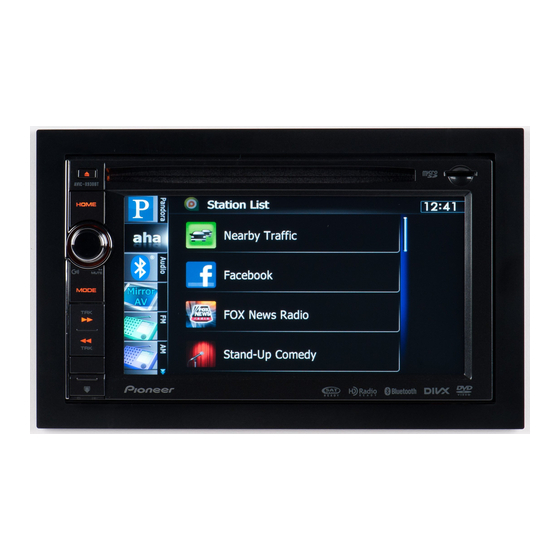
2.3 PANEL FACILITIES Checking part names and functions This chapter gives information about the names of the parts and the main features using the buttons. AVIC-X930BT, AVIC-X9310BT button Press to display the map screen while Press the button to activate voice op- the navigation function screen is dis- erations. - Page 14 Press and hold the Detach button, and AVIC-X930BT, AVIC-X9310BT : Multi-control (Volume knob/ /MUTE) slide it down. AVIC-F930BT : Multi-control (Volume knob/ /MUTE) Rotate to adjust the AV (Audio and Video) source volume. Press the center of Multi-control to hear the route guidance.
-
Page 15: Connection Diagram
2.4 CONNECTION DIAGRAM AVIC-X930BT/XNUC, AVIC-X9310BT/XNUC AVIC-X930BT/XNUC... - Page 16 AVIC-F930BT/XNAU AVIC-X930BT/XNUC...
- Page 17 AVIC-X930BT/XNUC, AVIC-X9310BT/XNUC AVIC-X930BT/XNUC...
- Page 18 AVIC-F930BT/XNAU AVIC-X930BT/XNUC...
- Page 19 AVIC-X930BT/XNUC...
- Page 20 AVIC-X930BT/XNUC...
- Page 21 AVIC-X930BT/XNUC...
- Page 22 AVIC-X930BT/XNUC...
-
Page 23: Basic Items For Service
3. BASIC ITEMS FOR SERVICE 3.1 CHECK POINTS AFTER SERVICING To keep the product quality after servicing, please confirm following check points. Procedures Item to be confirmed Confirm whether the customer complain has The customer complain must not be been solved. reappeared. -
Page 24: Pcb Locations
3.2 PCB LOCATIONS DVD Core Unit Connect PCB IF PCB Keyboard PCB AV Unit CC Monitor Unit (Service) SD PCB Unit Number : CWN5681(UC) : CWN5684(AU) Unit Name : AV Unit IF Unit Consists of Keyboard PCB IF PCB SD PCB Unit Number : CWN5866(UC) : CWN5869(AU) Unit Name... -
Page 25: Jigs List
3.3 JIGS LIST IF PCB Use the cable used in this product. GGF1158 GGF1656 DVD Mechanism Module(LS1) GGD1170 AV Unit GGD1222 GGD1250 GGD1633 CC Monitor Unit (Service) AVIC-X930BT/XNUC... -
Page 26: Cleaning
Jigs List Name Jig No. Remarks DISC GGV1025 Skew adjustment, Check points after servicing, Inspection method of Pickup Unit DISC TCD-782 Inspection method of Pickup Unit 20P FFC Extension Cable GGF1158 AV UNIT <---> IF PCB 40P FFC Extension Cable GGD1170 AV UNIT <--->... - Page 27 AVIC-X930BT/XNUC...
-
Page 28: Block Diagram
4. BLOCK DIAGRAM 4.1 OVERALL CONNECTION DIAGRAM Note: When ordering service parts, be sure to refer to " EXPLODED VIEWS AND PARTS LIST" or "ELECTRICAL PARTS LIST". RCA TER JA18 CN5607 SD CARD Connector CC MONITOR UNIT (SERVICE) CODE ASS'Y PS/IF SECTION CDE9389 CN18... - Page 29 CODE ASS'Y MIC ASS'Y POWER SUPPLY TERMINALS CPM1083 UC : CDP1307 AU : CDP1306 IP-BUS IN RCA TERMINAL FUSE SYSTEM P.BREAK REVERSE REMOTE SPEED RR- RL+ ILM ACC B.UP PULSE JA1891 JA1001 JA2351 JA1831 UC only AV UNIT PS/IF SECTION DVD MECHA SYSTEM uCOM SECTION MODULE...
-
Page 30: Block Diagram
4.2 BLOCK DIAGRAM AV UNIT(1/2) RF FRONT END IC IC2001 REARVOUT TDA7706 JA2061 TUN_L_HIT TUN_L RFIN DACOUTL LNAIN PINDIN IP_L IP_LG FMMIXIN1 TUNPCK I2CSCL TUNPDA AV_LOUT I2CSDA RDSINT GUIDE RDSINT TUNRST RSTN JA1831 IPL+ IP_L IPL- IP_LG IP-BUS DRIVER IC1831 HA12241FP AU84 IPBUS+... - Page 31 JA1891 VIDEO REARVOUT VIDEO VGND SW OUT MUTE TUN_L IN5L Pre_SWL Q1793 LGND Q1801 POWER AMP IP_L IN4L+ IC1051 IP_LG IN4L- PA2030A JA1001 Front_L AV_LOUT1 OUT4(+) IN2L GUIDE OUT4(-) IN3L Rear_L OUT2(+) Mic_in SYSPW5 TO 2/2 STBY OUT2(-) E-VOL/AUDIO BREM H-SW/VOS-DET SELECTOR AMP MUTE...
- Page 32 AV UNIT (2/2) SYSTEM u-COM IC1302 (2/2) :PEG745A8 CN2301 :PEG747A8 (3/3) P120 KDT0 EEPROM KDT0 SENSE1+ IC1303 KDT1 KDT1 SENSE1- S-93C56BD0I-I8 KDT2 Q1204 KDT2 MOVITEMP CCTEMPIN FCONT_C FCONT_C CCD5 ILMRST ILMRST ILMSDA ILMSDA DC/DC ILMCK CONVERTER VD5CONT ILMSCL VD5CONT IC1201 LTC3850IGN CTOSYS Q1205...
- Page 33 KEYBOARD PCB DETACH CN2902 S3001 DETACH P1201 NKBUP KEY MATRIX KEY2 S3004, S3005, S3006, KEY1 S3007, S3008 VOLUME S3003 KEY0 CN3303 ROT_IN1 ROT_IN2 ILMR1 ILMG1 ILMB1 D2902 ILMV D2901 JA2901 CN2901 BT MODULE NKBUP VDD5 IC1111 NKBUP BD3931FP VDD33 C1091 200B33-M5 VDD5 ON/OFF...
- Page 34 DVD CORE UNIT NRES VIDEO MN2DS0 NRES NRES FLASH 16M IC1401 CWW3159 NRES RESET FLASH 16M IC1402 CWW3160 NRES RESET SDRAM IC1480 IS42S16400F-7TL CONNECT PCB MOTOR DRIVER IC1201 LS1 MECHA UNIT BD8231EFV CN1201 CN701 CRG/LE- VHALF CRG- SL/LDO- VHALF LOADING/CARRIAGE CRG+ CRG/LE+ MOTOR...
- Page 35 CN1901 NRES XRESET VIDEO+AUDIO IC1501 AUDIO 2CH ANALOG OUT MN2DS0018MA IC1801 PCM1753DBQ NRES SRCK LOUT ANALOG LOUT SRCK VOUTL ADOUT ADOUT DATA LRCK LRCK LRCK SDODAC ISC_SCL SDODAC SCKDAC I2C_SDA SCKDAC CP_Reset RESET LTDAC LTDAC IFCOUT DACCK DACCK CN1521 COMPOSITE COMPOSIT STANBY STANDBY...
- Page 36 IF PCB CN291 VTR2L VTR2LG VTRIN2V VTRIN2VG CN1851 RLOUT2 CN103 Q261 Q262 IR REMOTE SWVDD33 IC101 REMIN RS-470 Q264 PREMUTE (BCV) (BCVG) TELMUTEIN FANON FANCONT CCD5 USB5 IC381 IC382 BD9008F BD82001FVJ NKBUP NKBUP OUT1 USB5 CN2401 OUT2 CCDIO3 EN/SYNC OUT3 DTV3 IC221 IC223...
- Page 37 CN261 VTR2L VTR2LG VTRIN2V VTRIN2VG RLOUT2 CORD ASSY Q263 AV(PREOUT) TERMINALS KMODE KMODE CTOEX HYOKA (HYOKA) EXTOC BCVG TELMUTE CN201 FAN CONTROL P201 FANV Q201, Q202 FANON Q203, Q204 Q205 FANCONT JA241 WREMIN1 WIRED WREMIN2 REMOTE GNDD CN231 USB 5V USB5 VOUT V_RETURN...
- Page 38 CC MONITOR UNIT(SERVICE)(1/2) CN4602 X_VIP_PXD[0 - 7] AIN1 VIDEO DECODER IC5513 SD_DATA[0] - SD_DATA[3] AK8859VN X_VIP_DVALID_FID AC18 X_VIP_VSYNC VD_F SD_CMD AC19 X_SD_CMD_1 X_VIP_HSYNC SD_CL X_SCL1 AC17 X_SD_CLK_1 X_VIP_PXCLK DTCLK X_ SDA1 AB17 X_VIP_PXD[10] SD_DET X_SD_CD_B_1 X_SCL1 SCL_1 X_SDA1 SDA_1 iPod authenticatrion coprocessor IC (1/2) IC4001 IC4701...
- Page 39 DDR SDRAM(512Mbit x 4) CN5607 (3/4) IC4401 CPUWDT X_LDD[16] H5DU5162ETR-E3C X_LDD[17] CN3300 X_LDD[18] PCHNG X_LDD[19] X_SCL1 IC4402 GMUTE X_GPIO[1] X_ SDA1 BOTTOM H5DU5162ETR-E3C AB14 ASENRQ X_GPIO[6] AA14 BSENRQ X_GPIO[7] IC4404 SYSTOC X_RXD_2 H5DU5162ETR-E3C AD_SDA0 X_SDA_0 processor IC AD_SCL0 X_SCL_0 IC4405 CN5605 H5DU5162ETR-E3C PI_SOMI...
- Page 40 CC MONITOR UNIT(SERVICE)(2/2) POWER ON RESET IC4217 S-80835CLMC-B6U IO_ON CCD5 VD18 IC4211 NJM2878F3-18 CP18 VD18 VOUT CCD3 CONT Q4210 CCD3 Q4211 CCD2.5V IC4204 LTC3412AEFE P4202 CCD25 SW_1 SVIN CCD5 SW_2 PVIN_1 SW_3 PVIN_2 CCD25_PLLON SW_4 Q4218 CN5607 RUN/SS CCD25_PLLON (4/4) PWRBL Q4207 CCD3...
- Page 41 SD PCB CN5951 CN5952 SD_DATA[0] - SD_DATA[3] SD_DET SD_DET MICRO SD CARD CN4602 SD_CL SD_CL SD_CMD SD_CMD CN2301 AVIC-X930BT/XNUC...
-
Page 42: Power Supply System Figure
4.3 POWER SUPPLY SYSTEM FIGURE AV UNIT BUPV :POWER SUPPLY :Model & Delivery 0.5 A/1.6 W 0.11 A/1.045 W AD3V(Reg) VDD5(Reg) BH30NB1 Constant WHFV PowerSupply5V 5 LEVEL SHIFT BD3931HFP GYRO Sens TC74VHCT541AFST CSX1147 PLLON XV8100CB 2 mA 10 000 uF/16 V 3.0 V±0.15 V TYP:1.7 mA SWVDD5... - Page 43 G Sensor GYRO Sensor Temp Sensor ADS7828E S-58LM20A-N4 CSX1149 CSX1147 LIS344ALH XV8100CB 3.0 V±0.15 V 3.0 V(2.4 V–3.6 V) 3.0 V(2.7 V–5.5 V) 3.0 V TYP:1.7 mA TYP:0.68 mA TYP:0.0045 mA (2.7 V–3.6 V) MAX:0.85 mA MAX:0.006 mA TYP:0.225 mA MAX:0.32 mA RESET IC S-80929CNMC...
- Page 44 TO IF PCB CCD5/CCD3 LTC3850IGN 5.21 V:Max1.6 A 3.43 V:Max1.36 A CCD5 FET(7 A) BUPV CCD3 NAVION5, DDCLK2 RF5V±0.25 V max300 mA 0.8 A/1–1 TU5(Reg) 300 mA/1 NJM2846DL3-05 TUON1 (1 A/2–18 W) 400 mA/2.68 W ACC84(Reg) 8.4V NJM2388F84 ACCPW5 AVIC-X930BT/XNUC...
- Page 45 TO IF PCB 100 mA 1500 mA TO CC MONITOR UNIT 1360 mA ax300 mA FM/AM Tuner 0.8 A/1–10 W (Silicon Tuner) 300 mA/1.05 W Silicon Tuner PowerSupply RF5 V±0.25 V 300 mA(MAX) E-VOL 8.4 V typ:66.8 mA PML020A max:86.3 mA AVIC-X930BT/XNUC...
- Page 46 (1 A/2–18 W) AV4. 134 mA/0.9 W NJM2 AU84(Reg) 450 mA (Center V 8.4 V NJM2388F84 SYSPW5 MAX 120 mA TO CC MONITOR UNIT ILMV SOC 250 mA CEK1276 LS1VDD (D/D) BUPV 5V LT3505 VD5CONT System microco MT81V(D/D) 8.1 V BD9781HFP SOC 3.15 A 1.506 A...
- Page 47 MUTE Circuit 5.7 mA Guide, P-Amp. RN4982*3 AV4.3(4.2 V) typ 3 mA NJM2125F max 5 mA 1.6 mA max NAVI ISOLATOR (Center Voltage for Audio) BA4558RFVM SELECTOR AK4223VQ GND SELECT 1 mA max typ:33 mA RN4982 max:50 mA IMH23 TOR UNIT MAX 461 mA TYP 220 mA DVD MECHANISM...
- Page 48 CC MONITOR UNIT From AV UNIT CCD5 IC4205 CCD1.2 V CCD12 LTC3412A PRE_ON 1.5k 1.5k IC4219 BD6522 Q4214 CCD3IOON PLL_ON IO_ON PLL_ON Q4218 CCD25 IC4204 CCD2.5 V LTC3412A IO_ON NAND3 IC4361 NAND3 S-1132B33-M5 PRE_ON CCD3 IC4209 LCD25 LCD25 NJM2878F3-25 AVIC-X930BT/XNUC...
- Page 49 IC4001 SiRF_Prima TT4421 3.3 V VDD_LVR 2.3 V–3.6 V TYP:1 mA 3.3 V VDDIO_RTC 3.3 V(2.3 V–3.6 V) TYP:1 mA 1.2 V CORE VDD_PRE 1.2 V±0.06 V TYP:50 mA 1.2 V VDD_PDN 1.2 V±0.06 V TYP:800 mA Q4217 PLL12 1.2 V VDDA_PLL 1.2 V±0.06V TYP:10 mA VDD_PLL 1.2 V±0.06 V TYP:10 mA PLL_ON...
- Page 50 Sequence generation IC4208 LCD15 IC4216 LCD15 RST1 NJM2878F3-15 PRE_ON 3.0 V IC4217 RST2 IO_ON 3.5 V IC4281 RST3 PLL_ON 4.4 V Q4209 X_SD_VCC_O (for SiRFprima IC4211 VD18 VD18 NJM2878F3-18 IO_ON PWRBL IC5508 BL DRIVER OZ9990IRN MBLPW IC3300 LED DRIVER GREEN NJU6062V BLUE ILMV...
- Page 51 LCD15 Ipod 3.3 V(1.8 V–3.6 V) authenticatrion MAX:10.0 mA 3.3 V IC4701 (2.0B_Class4) 341S2162 R4381 AC97-CODEC 3.3 V(A) 3.3 V(2.7 V–3.6 V) IC4654 3.3 V(D) MAX(A):13.6 mA WM1616LGEFL MAX(D):18.4 mA 3.3 V SD Slot 3.3 V(2.7 V–3.6 V) Micro MAX:200 mA X_SD_VCC_ON (for SiRFprima) VIDEO-Decoder...
- Page 52 IF PCB IF PCB FROM AV UNIT CCDIO3 NKBUP SWVDD33 CCD5 100 mA 10 mA 100 mA 100 mA 1500 mA K-MODE UC only CAN-BUS IR-REMOTE Circuit RS-470 2 mA EU5 only AU only GPS-RF GRF3I- GPS33 0336B BU33TA2WNVX TYP:14.9 mA MAX:15.4 mA GPS_SAMPLE buffa _CLK...
-
Page 53: Diagnosis
5. DIAGNOSIS 5.1 OPERATIONAL FLOWCHART AVIC-X930BT/XNUC... -
Page 54: Inspection Method Of Pickup Unit
5.2 INSPECTION METHOD OF PICKUP UNIT Disc to be used CD-DA: TCD-782 DVD-Video: GGV1025 Execution method Replace the PICK UP START SKEW ADJ. LD turned on? Check parts Check point: Check point: RF level check LD current check AS MAX check LD current check Is it OK? Is it OK? - Page 55 LD current check Check Status: [Foucs closed] of TEST MODE Disc Check Point Threshold Remarks: LD current GGV1025 DVDLD1-VCC5_3 60 - 390 (mV) 10 - 65 (mA) Expansion NO. Disc Check Point Threshold Remarks: LD current TCD-782 CDLD1-VCC5_3 150 - 900 (mV) 10 - 60 (mA) Expansion Notes: Please pay attention to the laser diode damage by static electricity.
- Page 56 ASMAX check ASMAX value shows the value of RF level. Status: [Foucs closed] of TEST MODE Disc Check Point Threshold Remarks: 8 digits value of Only four last digits are more than GGV1025 ASMAX displayed according to on display 0000 0B00 the product.
-
Page 57: Diagnosis Flowchart
5.3 DIAGNOSIS FLOWCHART AVIC-X930BT/XNUC... -
Page 58
Check 1: Standby OK?
Check the voltage at the “STANBY” test point while the power is on. Use the “DGND1” test point at the reference. Specification value Check point Module No. Unit STANBY-DGND1 VCC33 V- 0.6 V or more Side A DGND1 STANBY... - Page 59 Check 2: Is VDD5 (VCC33, VCC12) power supply voltage OK? IC1401 FLASH power supply (Data) VCC33 (= 3.3 V) IC1402 FLASH power supply (Program) IC1004 IC1481 SDRAM power supply 3.3 V output regulator IC1501 DV5U power supply IC1005 VCC12 (= 1.2 V) IC1501 DV5U power supply DC/DC converter 1.2 V output...
-
Page 60
Check 3: Reset OK?
Check the voltage at the “XRES” test point while the power is on. Use the “DGND1” test point at the reference. Check point Module No. Specification value Unit 1 XRES-DGND1 VCC33 × 0.7 or more Side A DGND1 NRES... -
Page 61
Check 4: Is VSENS OK? CN1901 HOST I/F IC1501 R1004, DV5U R1007 IC1004 Regulator IC1005 VCC12 DC/DC converter STANBY XRES Fig 4.1: Power supply configuration and VSENS
Check the voltage at the “VSENS” test point while the power is on. Use the “DGND1”... -
Page 62
Check 5: 27 MHz Normal?
Each clock is created inside the IC1501 using the 27 MHz master crystal oscillator (X1501). IC1501 DVD-LSI OSCO X1501 27 MHz OSCI crystal VCC33 VCC12 Fig 5.1: Clock configuration Turn the power on, and check with DGND being the reference. In case of NG, check the applicable line, periphery of IC1501, soldering of the peripheral components and defective components. -
Page 63
Check 6: Is SDRAM I/F OK?
In order to secure the MPEG stream data as the buffer, the capacity of communication I/F SDRAM between the LSI and the memory is 64Mbit. Be careful as XCSM, XWE, XCAS and XRAS of IC1480 are called differently in IC1501, namely NCSM, NWE, NCAS, NRAS. -
Page 64
Check the conductivity at “check point 1” and “check point 2” without power. In case of NG, check the soldering and defective components throughout the “output t input” of the applicable section. Signal name Check point 1 Check point 2 Specification value IC1480 23pin... - Page 65 Side B Check point 1 (IC1480) Side A Check point 2 (IC1501) Fig 6.2: SDRAM I/F check point AVIC-X930BT/XNUC...
-
Page 66
Check 7: Is VD8, VCC5 power supply voltage OK? VD8_1 F.E. driver system IC1002 VCC5 (= 5.0 V) VD8_2 Power supply REG IC for PU for VCC 5 V. Fig 7.1: Power supply configuration
Check the voltage at the “VD8_1, VD and VCC5_1” test point while the power is on. Use the “PGND3 and AGND1”... -
Page 67
Check 8: Is AVCC5 voltage OK? IC1003 AVCC5 (= 5.0 V) IC1801 REG IC Audio-DAC for AVCC 5 V. Fig 8.1: Power supply configuration
Playback DVD-REF-A1 TITLE 1 and check the voltage at the stylus. Check with PGND and GNDAU being the reference. Check point Module No. -
Page 68
Check 9: Is DACCLK normal?
DACCLK for Audio-DAC is created by IC1501 using the 27 MHz master crystal oscillator (X1501). IC1501 X1501 DVD-LSI IC1801 DACCLK Audio-DAC 27 MHz crystal VCC33 VCC12 Fig 9.1: Clock configuration DVD: DVD-REF-A1 TITLE 1 CD: Playback a normal CDDA. - Page 69 Side B Check point 1 (DACCK stylus) Side A Check point 2 (IC1501 148 pin) DGND2 Fig 9.3: 27 MHz, DACCLK check point AVIC-X930BT/XNUC...
-
Page 70
Check 10: Is the audio circuit OK?
The serial 3 lines digital output + DACCLK, output from DVD-LSI (IC1501), are converted to analog audio signal at Audio-DAC (IC1801) and are output from the HOST I/F (CN1901). Simultaneously, the analog MUTE signal is also output from DVD-LSI (IC1501) via the HOST I/F. The digital audio signal (IECOUT), output from DVD-LSI (IC1501). - Page 71 Side A DGND2 ADOUT LRCK Side B SRCK Fig 10.3: Serial 3 lines check points AVIC-X930BT/XNUC...
- Page 72 The following checks shall be conducted using the following measurement circuits with GNDAU1 being the reference. 47 kohm 47 kohm GNDAU1 Check point 1 (stylus) Specification value (rms) Reference waveform 1 400 ± 150 mV Waveform 4 1 400 ± 150 mV Waveform 4 Specification value is the root-mean-square value (rms).
- Page 73 Side A IEC DGND2 Fig 10.6: Digital audio signal (IECOUT) check point AVIC-X930BT/XNUC...
-
Page 74
Check 11: Is the video circuit OK?
Composite signal and component signal are output from DVD-LSI (IC1501), and are output from the HOST I/F (CN1901) via a buffer circuit. CN1901 HOST I/F IC1501 DVD_LSI Composite COMPOSITE Video section Fig 11.1: Video circuit ... - Page 75 Side A COMPOSITE GNDV Fig 11.3: VIDEO signal check point AVIC-X930BT/XNUC...
- Page 76 Check 12:How to judge whether the flash memory has reached its life or not. If the reaction to user operation is slow or operation is slow in general, there is a possibility that the flash memory has reached its life. Make judgment regarding the flash memory life by looking at the display of the LD energizing time.
-
Page 77
Check 13: 48 MHz Normal?
Each clock is created inside the IC1501 using the 48 MHz master crystal oscillator (X1501). IC1501 DVD-LSI X1950 48 MHz crystal USB_CLOCK VCC33 VCC12 Fig 13.1: Clock configuration Turn the power on, and check with DGND1 being the reference. In case of NG, check the applicable line, periphery of IC1501, soldering of the peripheral components and defective components. - Page 78 Side A IC1501 50pin DGND1 Fig 13.3: 48 MHz check point AVIC-X930BT/XNUC...
- Page 79 1.USB Memory: Play a song from USB memory and check D+ and D- with the DGND standards. 2.iPod: Connect iPod and check CP_RESET, SDA and SCL with the DGND standards until the pioneer log appears. Play a song from iPod and check D+/D- with the DGND standards.
- Page 80 Side A SDATA CP_RESET SCLOCK DGND2 AVIC-X930BT/XNUC...
- Page 81 AUDIO CH1:LO CH2:RO CH1:ADOUT3 Reference voltage: DGND2 1 V/div. 5 usec/div Reference voltage: GNDAU2 1 V/div. 500 usec/div G-> -> -> Waveform 1 Waveform 4 CH1:SRCK CH1:IECOUT Reference voltage: DGND2 1 V/div. 5 usec/div Reference voltage: DGND2 1 V/div. 500 nsec/div G->...
- Page 82 VIDEO [WHITE 100IRE] CH1:COMPO Reference voltage: GNDV1 200 mV/div. 10 usec/div Waveform 6 USB memory USB memory USB memory Reference voltage:DGND 1 ms/div 2 V/div Reference voltage:DGND 200 ns/div 2 V/div Waveform 7 Waveform 8 AVIC-X930BT/XNUC...
- Page 83 iPod iPod iPod Reference voltage:DGND 1 ms/div 2 V/div Reference voltage:DGND 200 ns/div 2 V/div Waveform 9 Waveform 10 iPod iPod Reference voltage:DGND 2 ms/div 1 V/div Reference voltage:DGND 20 ms/div 1 V/div CP_RESET DGND NRES Waveform 11 Waveform 12 iPod Reference voltage:DGND 500 us/div 1 V/div Waveform 13...
-
Page 84: Error Code List
5.4 ERROR CODE LIST Generation source Method of reset UART Source Eject Play Key Error status OSD *1 Meaning Disc (MSC) (iPod) Off/On Off/On A disc containing the unplayable NON-PLAYABLE DISC Format only USB device that doesn't correspond INCOMPATIBLE DEVICE USB device of format alone that UNPLAYABLE FILE cannot be reproduced... - Page 85 X: Cancel the error by operation. -: Error is not cancelled by operation. *: No setting *1 A content displayed on OSD. As for the items having multiple display patterns, the upper row is for the Japanese version Full GUI, and the lower row is for the Touch Panel model and Full GUI (English version).
-
Page 86: Connector Function Description
5.5 CONNECTOR FUNCTION DESCRIPTION iPod AV CONNECTOR RDS-TMC TUNER 14 13 13 : VTR2RG 1 : VTR2R 14 : VTR2LG 2 : VTR2L 10 : ACCDET 1 : USB- 3 : VTRIN2V 15 : VTRIN2VG 1 : SWBUP 11 : A_RETURN 2 : USB+ 4 : RROUT2 16 : REARG... -
Page 87: Service Mode
6. SERVICE MODE 6.1 TEST MODE 1. How to Select Test Mode Menu Key operations used at the test mode are the following six keys; Key Operation Key Allocation Cursor Up VOL UP Cursor Down VOL DOWN Page Change (Previous) LEFT Page Change (Next) RIGHT... - Page 88 3. Test Mode Menu Name of Test Item Overview of Test Display version information such as Navigation Software, Version Information Navigation Destination, Microcomputer Software, etc. Perform Error / Log View, File Copy and Clearing. Error / Log History Writing of Navigation Program / Platform/Boot Loader / IPL / System Microcomputer / BT Firmware.
- Page 89 Name of Test Item Overview of Test Display GPS positioning data, satellite information GPS INFORMATION acquired and error information. Version display of GPS driver / sensor. GPS assessment Reset GPS driver and perform clearing of backup GPS backup data clear data.
- Page 90 Name of Test Item Overview of Tes Display G Sensor, gyro value, power supply EXT CONNECTION TEST voltage, temperature and variation, CAM_ON terminal and installation status. Confirmation of microphone input line for audio MIC LINE TEST recognition. Confirmation of audio output line for SD / USB NAVI VOICELINE TEST Audio.
- Page 91 1. Version Information Obtain version information for assigned software and display the information on screen with list display. 1. Program Version [The first page] Item Item Contents Information Display PLATFORM version of system software OS part [ *.****** ]: Value of Version [NO_SET]: No information Version of product startup program [ *.****** ]: Value of Version...
- Page 92 2. Model Information [The second page] Item Item Contents Information Display PRODUCT NUMBER Product Model Number [ AVIC-X930BT/XNUC ]: North America LO Model (AVIC-X930BT/XNUC, AVIC-X9310BT/XNUC) [ AVIC-F930BT/XNAU ]: Australia LO Model [ NO_SET ]: No information NAVI INFORMATION Planning Model Number [ NX072/UC ]: North America LO Model (AVIC-X930BT/XNUC, AVIC-X9310BT/XNUC) [ NX072/AU ]: Australia LO Model...
-
Page 93
2. Error/Log History Perform displaying each error history, saving the history into storage and clearing the history. Menu Screen <
- > 1. Error History Show Display error history currently saved. 2. Log History Show Display execution log history currently saved. 3. Error / Log History Save Save histories of error, log and exception files into storage.
-
Page 94
2. Log History Show The execution log is the execution history when specific operation is performed. (Not errors) <
> Date : Time of error recorded TickCount : Value of counter started counts at OS startup. 1 count is corresponding to 1 millisecond. : Log information 3. -
Page 95
4. Error / Log History Delete Histories for error, log and exception are saved. <
> * If the copy processing results in failure, the fact it is failed is displayed on the screen. * You can also continue other inspection without turning OFF the power supply when the deletion is completed. However, take note that the exception history is not saved in that case. - Page 96 Select Storage Screen Select the program should be written from SD card or USB memory. Instruct the start of program writing. [Writing of navigation program] 4. SELF CHECK PROGRAM The connection status of function module installed in the product is displayed. In the case of non-connection, error is displayed and the target module is considered to be fault.
- Page 97 5. Touch Panel Check At the touch panel check, X, Y coordinates of location where touched are obtainable. When touched, the coordination value where touched is displayed as well as vertical and horizontal lines are illustrated with the cross point at the touched location. The coordination value is set as the original point at upper-left and X coordinate to the right and Y coordinate to the down, and maximum value of X coordinate is 800 and of Y coordinate is 480.
- Page 98 1. Line Touch Panel Test Touch the illustrated points in order. If touched incorrectly, + mark is displayed in red. When the touching proceeded to the final point of four (4), [OK] is displayed and the test is completed. When depressing [HOME] key, [NG] is displayed and return to the menu screen. Key operation Key assignment Return to Main Menu...
- Page 99 7. Monitor Test Mode Adjustment or test related to monitor is able to be performed. Menu Screen <
-
Page 100
2. Service Test No need to perform this ‘Service Test’ Flicker adjustment is done in a LCD unit, because LCD specification is changed It is possible to change the ‘COM_DC’ value on the screen, but it doesn’t affect the flicker of the screen. <
>... -
Page 101
4. Illumination RGB Test * This function does not operate for this model. <
> Contents Item Name Data-R R (Red) data value Data-G G (Green) data value Data-B B (Blue) data value E2PROM Write ON/OFF setting of writing to E2PROM 5. - Page 102 8. Key Test At the key entry test, key code of the hard key depressed, depressed/released status and key description are displayed. Retaining up to 12 histories is also possible. Test Screen The indication of each key allocated is shown below. When [HOME] key is depressed, however, it returns to the main menu.
- Page 103 9. Port Test At this test, port status of each item is displayed as Hi/Low. The following port status is able to be confirmed. Each description for port is as follows; 1. Detection of External RDS/MSNDirect Connection: At this port, the status of external RDS/MSNDirect connection detection port is displayed. Hi: Connection detected Low: Connection not detected 2.
- Page 104 10. Drive Maintenance In this test, each drive information is displayed and scan disc of NAND file is performed. Drive Information Drive Information Display Page When drive information failed to be obtained, “Drive Information failed to be obtained” is displayed and an error number is displayed subsequently. Error numbers and cause of errors are as follows;...
- Page 105 Scan Disc Screen for Executed Result of Scan Disc In the case of total error number being zero after the execution of scan disc, “There isn’t error on the volume” is displayed. AVIC-X930BT/XNUC...
- Page 106 11. File Maintenance This test provides the capability to manage files in each directory. In concrete terms, deletion of directory and execution of dumping are possible. Operation Screen for the First Phase The following 10 directories are becoming as the most significant directories. USER/NDATA/SD/SD2/SD3/SD4/USB/USB2/USB3/USB4 The current file path is displayed on the first line.
- Page 107 12. GPS Information At this test item, various values or status which is receivable from GPS are displayed. Screen Display * The First Page [Position] Positioning Status Satellite Vehicle Number in Acquisition Number of Satellite where positioning is possible Delay Time Horizontal Accuracy for HDOP Altitude Accuracy for VDOP GPS Time...
- Page 108 * The Second Page [Sv Stat] Satellite Vehicle Number in Acquisition Azimuth Elevation Angle Received Signal Level Positioning Status Accuracy * The Third Page [Diag] Channel : GPS Diagnostic Result Antenna Shot : Detection of Antenna Short Circuit Antenna Open : Detection of Antenna Open Circuit Backup Error : Detection of Backup Error AVIC-X930BT/XNUC...
- Page 109 * The Fourth Page [Err Info] Count Error Number Week of Error Time of Error Happened Day of the Week Happened 13. GPS Assessmentt Version information for GPS driver and sensor module are displayed on the screen. AVIC-X930BT/XNUC...
- Page 110 14. Clear GPS Backup Data Perform the resetting of GPS driver, clearing backup data and display the result on the screen. [At the time when the clearing of GPS backup is successful] [At the time when the clearing of GPS backup is unsuccessful] If GPS backup clearing results in failure, "ERROR!"...
- Page 111 16. SENSOR Test Sensor information (AD value, running status, installation status on main body and error at sensor learning) is displayed on the screen. G SENSOR / SIGMA : Display of G-sensor voltage value GYRO / SIGMA : Display of GYRO voltage value POWER : Display of power supply voltage TEMPERATURE...
- Page 112 17. Bluetooth Test Emit radio wave for Bluetooth authentication. Screen at the Time of Start First, display the following screen. Display sub menu screen after the completion of internal processing. Screen in Case of Error Return to the main menu with [HOME] key. This screen is also displayed when Bluetooth is internally used in other test.
- Page 113 1. External Analyzer Test Select [1. External Analyzer Test] from sub menu, the screen changes to the following by depressing [MODE] key and the radio wave is emitted. Screen under Radio Wave Emission Please start the measurement. Return to the sub menu with [HOME] key. 2.
- Page 114 There are six pages of selection patterns. Items 10, 11, and 12 on page 1 cannot be used. "MODE SET ERROR!!!" is displayed. Execute the test of these items on pages 4, 5, and 6 separately. (The content of the test is 10, 11, and 12 of items 36 to 44) Page 1 00.
- Page 115 Screen during the Emission of Radio Wave Selected test item and [Now testing…..] are displayed. Please start the measurement. Return to the sub menu with [HOME] key. 3. Output Frequency Channel Extended Test Radio wave in which 7 items are set in detail is emitted. Select item with [ ], [ ] keys and determine with [MODE] key.
- Page 116 3-1. Parameter Setting Select [1. Parameter Setting] and depress [HOME] key, then the screen becomes the item selecting screen below. Select item desired to be changed with [ ], [ ] keys and determine it with [MODE] key. Return to Output Frequency Channel Extended Test menu with [HOME] key. Setting screen for the selected item is displayed.
- Page 117 * Setting of [4. Single Frequency] and [5. TX Burst Period] are numerical entry so the display method becomes as follows; Move the digit of numerical value desired to be set (cursor indicated with blue color) with [ ], [ ] keys.
- Page 118 3-2. Execute After the necessary setting is completed, select [2. Execute] from Output Frequency Channel Extended Test menu, then the set radio wave is emitted by depressing [MODE] key. *The set content is able to be confirmed on the screen by depressing [HOME] key after selecting [1. Parameter Setting]. Please start the measurement.
- Page 119 18. NAND Test Perform the test on the read-write of NAND Flash. 1. Read Test Perform reading one sector by one sector from NAND Flash by assigning a starting sector number. This screen displays the following contents when error happens before getting into read test. In the Case of a Device Opening not Successful Fail to open device.
- Page 120 19. Clearing FLASH User Area Perform initialization/deletion of file data or variable which is used by the software of each navigation function (AV, One-Segment, GPS, etc.). A confirmation screen is displayed once before the clearing is executed. If [MENU] key is pressed, clearing / initialization is started. Target of Deletion Module Remarks...
-
Page 121
20. Audio Play Test Perform the confirmation of guidance audio output line by playing audio file. Audio is only played from the speaker in front. File Selection Screen <
> Path : Media where audio play file is placed is selectable. (NAND Flash/SD Card) File : File to be played is selectable. - Page 122 21. Image Test Display a specified image. 1. 10STEP IMAGE The grayscale bar of 10 step 11 tones is displayed. 2. PLAIN The displayed colors are eight colors; blue, red, pink, green, pale blue, yellow, white, and black (the color that is displayed for the first time in this item is blue). 3.
- Page 123 22. External Connection Test Display information regarding externally exposed terminals or sensors such as illumination terminals, vehicle speed pulse terminals, etc. Corresponding terminals are different depending on destination. The status of item shown on the following figure is updated for every 0.5 second. OK/NG Determination Condition GYRO Test OK/NG Determination of GYRO VOLTAGE...
- Page 124 Conversion table of CC part temperature and LCD monitor part temperature Monitor part CC part AD value Temperature AD value Temperature (HEX value) (HEX value) 03F6 -25.00 -60.0 03F2 -20.00 -55.0 03EC -15.00 -50.0 03E5 -10.00 -45.0 03DC -5.00 -40.0 03D1 0.00 -35.0...
-
Page 125
23. Speech Microphone Line Test Perform confirmation of speech microphone input line for audio recognition. Input from the microphone is output from guidance audio line via AC97 Codec. The confirmation of muting circuit on the guidance audio line is also confirmed by this test. <
>... - Page 126 24. NAVI Audio Line Test Perform the confirmation of audio line for SD/USB Audio. Sinusoidal wave of 1 KHz, 0 dB, is used for audio data. Audio is output from front/rear speakers. * The speaker output is set to large since this test is prepared for production line. Please be careful when you use it at service.
- Page 127 25. Subwoofer Line Test This is the test for the pre-output line of subwoofer. Sinusoidal wave of 100 Hz, 0 dB, is used for audio data. * Audio is also output from front/rear speakers during this test. * The speaker output is set to large since this test is prepared for production line. Please be careful when you use it at service.
- Page 128 26. Fan Control Test This is the item to test cooling fan installed at rear panel of product. In a normal situation, revolution rate is automatically changed depending on the interior temperature of a fan however FAN revolution rate is able to be confirmed regardless of temperature during the test execution.
- Page 129 27. Wired Remote Control Test Perform connection test for wired remote control. 1. Remote Control Key Code Input Information (REMOCON KEY CODE INFO) When depressing the key of connected wired remote control, the depressed key is displayed on the screen. 2.
- Page 130 1.2. Manufacturer Code Input Information Key code is displayed by depressing connected wired remote control key or test jig key. Update is not performed until another key is depressed. Key Allocation SOURCE 0x00010002 0x00010003 0x00010004 DOWN 0x00010005 LEFT 0x00010006 RIGHT 0x00010007 VOL UP 0x00010008...
- Page 131 2.2. Manufacturer Code Input Information (Display) Once the manufacturer code is obtained, the code is displayed. [*] is replaced by the following value. Manufacturer Code Value A: TOYOTA, DAIHATSU B: HONDA C: MATSUDA D: SUBARU E: MITSUBISHI F: SUZUKI * Manufacturer Code is obtainable only for Japanese Domestic model. Value of [FF] is displayed this model.
- Page 132 28. RTC Test Perform the test of RTC (Real-Time Clock) function and of external circuit function used when obtaining RTC count. 1. Time Setting Screen * This is not displayed when GPS antenna is connected. If this test is performed under the status of GPS antenna disconnected, [2008/10/01 12:00:00] is set as simulation time.
- Page 133 29. USB Check This is the item to check all of USB terminals. USB memory is used for the test. Check the performance by write -> read -> file comparison of 1 KB file automatically. Perform the test after inserting USB memory. The file to use for the test is automatically generated during the test so you do not have to prepare the file in advance.
- Page 134 30. SD CARD Test Perform file accessing to SD card and confirm the SD card is usable without any problem. The following screen is displayed during the test. The test content generates file for the test on the SD card, reads data out after data writing and compares the read out data with written data.
- Page 135 31. DATA COMMUNICATION TEST [OPEN] It is the item for confirming that the data communication terminal is opened. If the terminal is opened, the test result is OK. It is displayed before the inspection is started. The inspection is started by pressing the [MENU] key. Statuses of all terminals are inspected and the results are displayed.
- Page 136 32. DATA COMMUNICATION TEST [SHORT] It is the item for confirming that the data communication terminal is short-circuited. If the terminal is short-circuited, the test result is OK. It is displayed before the inspection is started. The inspection is started by pressing the [MENU] key. Statuses of all terminals are inspected and the results are displayed.
- Page 137 33. External Input Test Confirm the video input route or audio route is valid. The following three routes are targeted; I. iPod VIDEO [Video, Audio] II. External Input via RCA terminals (Video, Audio) Input video and audio to NAVI via video/audio input terminals and confirm the result with NAVI screen and speaker.
- Page 138 II. External Input via RCA Terminals [Video, Audio] When error happens, the following error message is displayed; Case 1. Failed to Setup VTR-ON. Input ON setting for microcomputer was unsuccessful. Case 2. Failed to Change Source of VTR. Source switchover for microcomputer was unsuccessful. Case 3.
- Page 139 34. Back Camera Test Confirm the signal line for back camera image is valid. “Back Camera Image” which was input from Camera Image Input Terminals at rear panel of the product is displayed. 1. Display via DECORDER This is the screen when back camera image is under display. The following error message is displayed when error happens;...
- Page 140 35. RGB Key Illumination Test Test the three (3) wires which brighten RGB illumination of hard key. It is OK when a white light is ON. This is the screen for RGB Key Illumination Test. RGB illumination for hard key glows white. The following error message is displayed when error happens;...
- Page 141 When Test is NG 37. Product Information The product information allocated to the product is displayed on the screen. 16 digit values sectioned into four (4) separated by a dot are displayed on the screen. Example: 0000.1111.2222.3333 AVIC-X930BT/XNUC...
-
Page 142: Dvd Test Mode
6.2 DVD TEST MODE Before shifting to the test mode, please insert the "DISC (CD-DA)". Operate the equipment by turning ON the parking. 1, 2 and 3 are invisible buttons. Display the test mode screen by carrying out following operations on this screen. Press areas of 1, 2 and 3 long in order. - Page 143 Legend: … Key operation … Operation state … The content displayed on the DVD mechanism (video only) Start of the test mode. 8 characters data is sent to the product side (HOST) by UART communication. TEST [Note] Higher level 4 characters only. Lower level 4 characters are spaces. LD power on time Simple FE test mode FE test selection...
- Page 144 2 x 00 0000 (3),(4) Focus Jump CRG +/- Power_OFF Tracking balance When L0 layer: 2000 0000 It operates while the key 2FFF 0000 When L1 layer: 2100 0000 is being pressed. 2B00 0000 : CRG+ TBAL coefficient (layer 0) 2C00 0000 : CRG- TBAL coefficient (layer 1) TE normalization coefficient (layer 0)
- Page 145 Legend: … Key operation EDC. Image of the test mode … Operational state … The content displayed on the DVD mechanism (video only) 8 characters data is sent to the product side (HOST) by UART communication. EDC1/2 test mode [Note] Image is the same for both EDC1 and EDC2. 0000 0000 EJECT operation [Note] Eject can be effected any time during the EDC test mode.
-
Page 146
Simple test mode The selection of the figure of each screen can be selected by "Key command for the test".
TEST MODE 1: LD ON 2: ASMAX 3: Skew Adjustment 4: Error Rate 5: CRG Move Outer 6: Eject Please Input Number 1 select 1: DVD Single Layer... -
Page 147: Disassembly
7. DISASSEMBLY While the photograph shown is slightly different from this model in shape, the disassembly procedure is the same. Removing the Monitor Assy (Fig.1, 2, 3) Remove the four screws. (Fig.1) Fig.1 Monitor Assy Remove the two hooks. (Fig.2) Remove the two hooks, and then lay the Monitor Assy on the front. - Page 148 Removing the CC Monitor Unit (Fig.4) Attention at assembly) When you attach Cord Assy, fix it with tape so that Cord Assy Remove the two screws does not contact the edge of the plate. and then remove the Holder and Cover. Tape Tape Holder and Cover...
- Page 149 Removing the DVD Mechanism Module (Fig.6, 7, 8) DVD Mechanism Module Disconnect the FFC.(Fig.6) Fig.6 Remove the five screws and then remove the Case Assy.(Fig.7) Fig.7 Remove the two screws Case Assy and then remove the DVD Mechanism Module.(Fig.8) Attention at assembly) The plate of the DVD Mechanism Module Fig.8 should come out from the Case.
- Page 150 Removing the Heat Sink (Fig.9) Heat Sink Disconnect the FAN Cable. Remove the two screws. Remove the six screws and then remove the Heat Sink. Fig.9 Removing the IF PCB (Fig.10, 11) IF PCB Disconnect the two FFC.(Fig.10) Remove the two screws Fig.10 and then remove the IF PCB.(Fig.11) Fig.11...
- Page 151 Disconnect the FPC from IF PCB Switch Push two points on right and left sides with fingers at the same time. However, if it is difficult to push the two points at the same time for the product, push one side at once. In that case, FPC is removed at a tilt, however, do not pull it at a tilt extremely.
- Page 152 How to have it 1.Have a specified part. Handling OK Handling NG AVIC-X930BT/XNUC...
- Page 153 Mecha Module_Bringing into the Clamp State with No Disc Loaded 1. Remove the relay FFC from the connector on the module PCB side (Fig. 1). (Precaution) When it is difficult to apply 4V to the motor in procedure 2 below, remove the connector on the relay PCB side, then remove the FFC, and remove the solder of the CRG motor lead and apply voltage to the lead.
- Page 154 CRG Mecha_Bringing into the Clamp State with No Disc Loaded 1.Remove the T-case washer and then remove the drive gear. (Fig. 1) 2.Lift the clamp arm assy until it is in the state shown in Fig. 2_b (open-lock state). 3.Put your finger on the area A of Fig. 2_c and then slide it to the direction of the arrow (the direction of the playing state). 4.Push down the clamp arm.
- Page 155 Removing the Module PCB 1.Short-circuit two spots on the land of the pick up FPC. (Fig. 1) 2.Remove the pick up FPC and the relay FFC from the connector. (Fig. 2) 3.Temporarily attach the pick up FPC to the pick up rack. (Fig. 3) (in order to prevent the damage to the pick up FPC) 4.Remove the two PCB clinch screws and then remove the module PCB.
- Page 156 Removing the PU Unit 1.Hook the feed screw biasing spring on the temporary hook (Fig. 2b). Be careful not to get injured by the tip of the spring. 2.Hold the PU at the location A in Fig. 1 and slide and scoot it to the direction of the inner periphery. 3.As in Fig.
-
Page 157: Each Setting And Adjustment
8. EACH SETTING AND ADJUSTMENT 8.1 DVD ADJUSTMENT 1) Precautions This product uses 5 V and 3.3 V as standard voltages. If the reference voltage is connected to GND by The electrical potential that is the reference for signals, mistake, turn the regulator OFF immediately, or is not GND, but VREF (approximately 2.2 V) and VHALF turn the power OFF. - Page 158 - SKEW adjustment When one of the following replacements has taken place, SKEW adjustment for the pick up will be required. (1) Replacement of the pick up unit (2) Replacement of the spindle motor (3) Replacement of the carriage chassis (4) Replacement of the main shaft of the pick up unit Measurement equipment and tools/jigs: Oscilloscope Driver for SKEW adjustment ->...
- Page 159 There are two methods of making adjustment: a method of making adjustment through monitoring RF waves by the oscilloscope (method 1) and a method of making adjustment through checking the numerical value of the RF level by OSD (method 2). Adjusting procedure is shown below, but regarding how to start the test mode and the operating procedure, please refer to the clause on the service test mode.
- Page 160 Skew Adjustment 1: Power OFF RF Level : 000000 Please Input Number 9. Skew Adjustment Select “1: Power OFF.” Skew Adjustment 1: Power OFF RF Level : 000000 Please Input Number 10. TEST MODE Select “6: Eject.” TEST MODE 1: LD ON 2: ASMAX 3: Skew Adjustment 4: Error Rate...
- Page 161 Disc Detection Arm 13. CRG Move Outer Select “1: DVD Single Layer.” CRG Move Outer 1: DVD Single Layer 2: DVD Dual Layer 3: CD 4: CD-RW 5: Return Please Input Number The pickup moves to the outer periphery. Apply the adhesive to fix the skew, the resonance adhesive and the screw lock. Refer to the next page regarding the locations of adhesive joining.
- Page 162 Locations to make SKEW adjustment Locations to adhere the SKEW 1,2,3: GEM1033 AVIC-X930BT/XNUC...
- Page 163 Bond for resonance 4:Three Bond 1530 adhesive Bond for locking the screw 5,6 : Three Bond 1401M Bond for locking the screw AVIC-X930BT/XNUC...
- Page 164 Precautions on handling the PU *Precaution: Do not touch those shaded areas in the following figures. Hologram (Beware of the static) Do not touch the optical part RF level adjusting part Do not touch the spring AVIC-X930BT/XNUC...
- Page 165 AVIC-X930BT/XNUC...
-
Page 166: Exploded Views And Parts List
9. EXPLODED VIEWS AND PARTS LIST OTES : Parts marked by " * " are generally unavailable because they are not in our Master Spare Parts List. The > mark found on some component parts indicates the importance of the safety factor of the part. Therefore, when replacing, be sure to use parts of identical designation. - Page 167 CONTENTS OF IM CD-ROM (Operation Manual), CPJ1334 Part No. Language * CRB3610 English * CRB3611 French * CRB3618 English All operation manuals are supplied in PDF files by the CD-ROM. Regarding the availability of paper manual, contact Pioneer Service representative in your region. AVIC-X930BT/XNUC...
-
Page 168: Exterior (1)
9.2 EXTERIOR (1) (1/2) (2/2) AVIC-X930BT/XNUC... - Page 169 (1) EXTERIOR (1) SECTION PARTS LIST Mark No. Description Part No. Mark No. Description Part No. Cord Assy CDE9389 Screw BSZ26P060FTC Bluetooth Module CWX4140 CNQ4273 LCD Panel CWX4022 CNQ4274 Grille Unit See Contrast table (2) Screw AMZ20P040FTC Screw BPZ20P080FTC Knob Unit CXE3932 Spring YBL5010...
-
Page 170: Exterior (2)
9.3 EXTERIOR (2) AVIC-X930BT/XNUC... - Page 171 (1) EXTERIOR (2) SECTION PARTS LIST Mark No. Description Part No. Mark No. Description Part No. Bracket CND5933 Screw ASZ26P060FTC Bracket CND6117 Screw BMZ25P040FTB Sheet See Contrast table (2) Screw BMZ26P040FTC Heat Sink CNR2097 Screw BSZ26P050FTB IF Unit See Contrast table (2) Screw BSZ26P060FTC Holder...
-
Page 172: Dvd Mechanism Module
9.4 DVD MECHANISM MODULE ( C ) ( C ) ( C ) ( B ) ( A ) ( A ) ( C ) ( A ) ( A ) ( C ) ( A ) ( C ) ( C ) ( C ) ( C ) - Page 173 DVD MECHANISM MODULE SECTION PARTS LIST Mark No. Description Part No. Mark No. Description Part No. Holder CNW1195 Screw BMZ20P020FTC Screw BSZ20P040FTC Damper CNW1197 Screw(M2 x 4) CBA1835 Damper CNW1198 Washer CBF1038 Connect PCB CWX3618 Spring CBH2860 ••••• ••••• Spring CBH3010 Spring CBH3011...
- Page 174 ( A ) ( A ) ( C ) ( C ) ( C ) ( C ) ( C ) ( C ) ( C ) ( A ) ( A ) ( A ) (A) : GEM1045 (B) : GEM1038 (C) : GEM1024 AVIC-X930BT/XNUC...
- Page 175 AVIC-X930BT/XNUC...
-
Page 176: Schematic Diagram
10. SCHEMATIC DIAGRAM 10.1 AV UNIT (PS/IF SECTION)(GUIDE PAGE) Note: When ordering service parts, be sure to refer to " EXPLODED VIEWS AND PARTS LIST" or "ELECTRICAL PARTS LIST". Large size SCH diagram Guide page NAV5 Detailed page R1223 F1201 >... - Page 177 AV UNIT (PS/IF SECTION) NAVI KEEP D1072 RF501B2S NAVION5 SP OUT SVD3 SWVDD33 FM:+29.56 dBs Q1101 AM:+29.56 dBs LSA1576UB > NAVI(USB/SD):+34.31 dBs G1267-A P1201 NAVI(BT-Audio):+34.98 dBs GNDD R1103 LS1:+34.98 dBs IC1091 CEK1259-A IP-BUS(UC):+34.31 dBs 2.2k SOC(3.15A) S-1200B33-M5 VDD33 i-Pod(aha):+34.40 dBs VTR2:+34.33 dBs Q1102 VOUT...
- Page 178 CODE ASS’Y POWER SUPPLY AVIC-X930BT/XNUC...
- Page 179 AVIC-X930BT/XNUC...
- Page 180 AVIC-X930BT/XNUC...
- Page 181 AVIC-X930BT/XNUC...
-
Page 182: Av Unit (System Ucom Section)(Guide Page)
10.2 AV UNIT (SYSTEM uCOM SECTION)(GUIDE PAGE) SPEED S TUNER VICS R1487 R1485 STODTV STODTV DTVVSEN DTVVSEN FEPW FEPW C1472 DTV_WDT DTV_WDT 1000p/50 R1475 DTV_RST DTV_RST GNDD 100k FCONT_D FCONT_D Q1471 IC1471 R1476 LTC114EUB DTVTOS NJM2904M DTVTOS R1474 DTV_TSEN DTV_TSEN R1477 DTVANTPW DTVANTPW... - Page 183 SPEED SENSE AV UNIT (SYSTEM uCOM SECTION) R1487 CCD5 R1485 SWVDD5 C1472 1000p/50 R1475 100k CDD5 CCD5 CCD5 R1476 R1474 SWVDD5 SWVDD5 SWVDD5 C1473 R1483 VDD33 VDD33 R1477 0.1u/16 VDD33 IC1471 SWVDD33 SWVDD33 NJM2904M SWVDD33 VDD5 VDD5 Q1472 LTC114EUB PCNG FV33 FV33 FVDETO...
- Page 184 AVIC-X930BT/XNUC...
- Page 185 AVIC-X930BT/XNUC...
- Page 186 AVIC-X930BT/XNUC...
- Page 187 AVIC-X930BT/XNUC...
-
Page 188: Av Unit (Audio Section)(Guide Page)
10.3 AV UNIT (AUDIO SECTION)(GUIDE PAGE) VDD5 MUTEBUP AU84 HIVOLT14 HIVOLT SYSTEM AUDIO AV SEL OUTPUT D1691 NAVI(USB/SD):+2.21 dBs NAVI(BT-Audio):+0.88 dBs AEQ/AUX SW D1692 LS1:+4.88 dBs SWVDD5 i-Pod(aha):+1.30 dBs R1876 VTR2:+2.23 dBs GNDA GNDV R1725 R1726 VTR1:+2.21 dBs Q1861 Q1862 R1781 R1782 R1862... - Page 189 AV UNIT (AUDIO SECTION) AV SEL OUTPUT NAVI(USB/SD):+2.21 dBs NAVI(BT-Audio):+0.88 dBs LS1:+4.88 dBs i-Pod(aha):+1.30 dBs VTR2:+2.23 dBs VTR1:+2.21 dBs AV SEL OUTPUT2(Rear) LS1:+2.88 dBs iPod(aha):+1.30 dBs L1691 AVOUT VTR2:+2.23 dBs VTR1:+2.21 dBs REARVOUT GNDA L1692 DUAL ZONE 4.7u R1751 R1753 C1751 R1755 CCG1201-A...
- Page 190 AVIC-X930BT/XNUC...
- Page 191 IP-BUS IN (LIGHT BLUE) AVIC-X930BT/XNUC...
- Page 192 AVIC-X930BT/XNUC...
- Page 193 AVIC-X930BT/XNUC...
-
Page 194: Av Unit (Tuner/Vics Section)(Guide Page)
10.4 AV UNIT (TUNER/VICS SECTION)(GUIDE PAGE) RF5V ± 0.25V DSP3.3V ± 0.16V DSP1.1V ± 0.05V WWR C-TUN UNIT U1951 1901 - 2200 CWE22 REFERENCE NUMBER LIST 1901 - 1910 : ANT8V to RFGND 1921 - 1930 : TU33 1931 - 1940 : TU11 1941 - 1950 : TU5 1951 - 2000 : HD Radio GNDRF... - Page 195 AV UNIT (TUNER/VICS SECTION) RF5V ± 0.25V max300mA DSP3.3V ± 0.16V max155mA DSP1.1V ± 0.05V max825mA TUN4.2V R C-TUN UNIT CWE2254 OUTPUT:4.19V L2142 405.405kHz or 384.615kHz BTH1110-A-T IC2141 TU42 10uH LT1912EMSE TUNCS L2141 TUNCS CTH1398-A C2143 TUNCLK TUNCLK BOOST 0.47u/16 CN1951 TUNDO TUNDO...
- Page 196 AVIC-X930BT/XNUC...
- Page 197 AVIC-X930BT/XNUC...
- Page 198 AVIC-X930BT/XNUC...
- Page 199 AVIC-X930BT/XNUC...
-
Page 200: Av Unit (Sensor/Flap Section)(Guide Page)
10.5 AV UNIT (SENSOR/FLAP SECTION)(GUIDE PAGE) CN5607 CN2301 CKS6118-A R2454 L2351 DTF1106-A R2358 GNDD GNDBL GNDD GNDD GNDD R2353 JA2351 F2351 MICIN CKN1018-A MICGND GNDD MOT8 ILMV PWRBL VD8V AU84 NKBUP VDD33 CCD5 R2413 R2414 SWVDD5 CCD3 VDD5 => AD3 SWVDD33 IC2221 PLLON... - Page 201 AV UNIT (SENSOR/FLAP SECTION) CN103 CN2401 CN2402 CKS5732-A GND SELECT GNDSEL GNDV GNDD GNDD Q2441 C1 1 6 E1 B2 2 5 B1 E2 3 IMH23-T R2442 R2441 CCDIO3 GNDD VD8V GNDSEL AU84 NKBUP VDD33 For DTV CCD5 SWVDD33 CN2202 CCD3 AU84 R2429 NM...
- Page 202 AVIC-X930BT/XNUC...
- Page 203 AVIC-X930BT/XNUC...
- Page 204 AVIC-X930BT/XNUC...
- Page 205 AVIC-X930BT/XNUC...
-
Page 206: Keyboard Pcb
10.6 KEYBOARD PCB KEYBOARD PCB C2903 0.1u/50 C2901 0.1u/50 C2904 C2902 0.1u/50 0.1u/50 CN2902 CKS5856-A CCMonitor Side ILMV ILMV KDT0 KEY0 KDT2 KEY2 KDT1 KEY1 ILMR1 ILMR1 ILMG1 ILMG1 ILMB1 ILMB1 R3031 R3037 R3044 R3043 1.2k 2.4k 3.6k 6.8k VOLUME DETACH GNDD DETACH... - Page 207 AVIC-X930BT/XNUC...
-
Page 208: Dvd Core Unit (Guide Page)
10.7 DVD CORE UNIT (GUIDE PAGE) (2125) C1801 R1803 ROUT ADAC D1901 C1806 D1902 C1808 R1601 R1955 GNDAU1 R1954 GNDV C1673 27.000MHz R1602 GNDAU CSS1768 R1804 LOUT X1501 R1673 NM R1675 X2 3 GND2 (2125) R1679 GNDD R1670 R1671 GND1 R1603 C1601 AUDIO 2CH ANALOG OUT... - Page 209 DVD CORE UNIT FOCUS SERVO LINE TRACKING SERVO LINE VCC33 1000->1049 :POWER SUPPLY 1100->1199 CARRIAGE SERVO LINE 1200->1299 :ACT+SPDL R1601 1400->1449 :FLASH SPINDLE SERVO LINE AGND2 1480->1499 :SDRAM 1500->1599 :DVN(SYS) RF SIGNAL GNDA 1600->1669 :DVN(FE) 1670->1699 :DVN(BE) 1700->1749 :VIDEO R1602 1800->1849 :AUDIO (ANALOG) 1850->1899...
- Page 210 AVIC-X930BT/XNUC...
- Page 211 CXX2398 PICKUP UNIT (SERVICE) AVIC-X930BT/XNUC...
- Page 212 AVIC-X930BT/XNUC...
- Page 213 AVIC-X930BT/XNUC...
-
Page 214: Connect Pcb
10.8 CONNECT PCB CONNECT PCB CN701 CKS6003 GND_B GND3 GND2 GND1 HOME HOME1 HOME1_B HOME HOME_B S101 R101 HOME 8SNS CSN1081-A DSCSNS 8SNS HALL BIAS+ 8SNS1 8SNS1_B 8SNS0 8SNS0_B S103 R102 COIL W COIL U CSN1081-A COIL V CN1201 DSCSNS HALL W+ DSCSNS1 DSCSNS1_B... - Page 215 AVIC-X930BT/XNUC...
-
Page 216: If Pcb (Guide Page)
10.9 IF PCB (GUIDE PAGE) CN5608 CN2401 CN101 CN103 CKS6299-A CKS5732-A GNDD GNDD USBGND GNDD GNDD GNDV AU only IR REMOTE IC101 RS-470 R116 GNDD GNDD R141 D1 D2 D3 C101 R147 R137 NM R148 R131 R142 R117 R149 R118 R143 NM R133 GNDD... - Page 217 CN103 CN102 IF PCB CKS5732-A VTR2:+8.23 dBs VTR2R VTR2R VTR2L VTR2L F262 CCG1082-A-T VTR2V VTR2V FANCONT CXM1394 REARR REARROUT FAN MOTOR REARL > 5.9V 10.5V REARLOUT GNDD P201 CEK1254-A (SOC 1A) VTR2VG CN201 Q205 GNDD Q202 CKS4822-A 2SA1587(GRBL) 2SD1760F5(R) GNDD REAR OUT (Dual Zone) C263...
- Page 218 CODE ASS’Y PREOUT USB/iPod Connecto AVIC-X930BT/XNUC...
- Page 219 SB/iPod Connector AVIC-X930BT/XNUC...
- Page 220 AVIC-X930BT/XNUC...
- Page 221 AVIC-X930BT/XNUC...
-
Page 222: Cc Monitor Unit(Service)(Ps/If Section)(Guide Page)
10.10 CC MONITOR UNIT(SERVICE)(PS/IF SECTION)(GUIDE PAGE) CN5607 CKS6118-A SN4201 LCDTEMP AVSELOUT R4275 R4265 R4392 AVSELOUT GNDV VOUT GNDV GNDV GNDV F4205 LCDTEMP SHUT S-58LM20A-N4 GNDA GNDV SHUT GNDD GNDD MOVITEMP MONO GNDD MONO GNDD GNDA Temp.sensor to watch F4204 R4305 IC4214 NAVI_L CCG1162-A... - Page 223 CC MONITOR UNIT(SERVICE) (PS/IF SECTION) GNDD GNDD PLL12 PLL12 Q4217 LSA1576UB(QRS) RTC12 20mA RTC25 RTC33 CCA3_IOON CCD25_PLLON Q4220 14mA CCD12 CORE Q4216 Q4218 CCD25_PLLON LTC114EUB LSA1576UB(QRS) PLL_ON 50mA PLL12 CCD3_IOON (10k/10k) Q4219 GNDD CCD25 IO_ON (10k/10k) Q4207 LTC114EUB CCD12 (10k/10k) CCD25_PLLON GNDA PLL_ON...
- Page 224 AVIC-X930BT/XNUC...
- Page 225 AVIC-X930BT/XNUC...
- Page 226 AVIC-X930BT/XNUC...
- Page 227 AVIC-X930BT/XNUC...
-
Page 228: Cc Monitor Unit(Service)(Cpu Section)(Guide Page)
10.11 CC MONITOR UNIT(SERVICE)(CPU SECTION)(GUIDE PAGE) GPIO UART Power Power CORE Sensor ADC VDDPRE GNDD GNDD GNDA F4001 VTL1171-A VDDPDN VDDMEM L4002 R4068 CTF1736-A (2012) VREFMEM GNDD GNDD GNDD GNDD GNDD GNDD F4003 VTL1171-A VDDIO L4006 GNDD CTF1736-A GNDD GNDD GNDD X_XN X_YN... - Page 229 Power CC MONITOR UNIT(SERVICE) CORE (CPU SECTION) BT_module R4014 GND_PLL GNDD R4018 GNDD USBGND GNDD GPS_SGN GPS_SGN Mode Configuration X_MCLKB_O GPS_MAG X_MCLKB_O GPS_MAG Working Mode Sub Mode Feature1 Feature0 X_MCLK_O GPS_CLK X_MCLK_O GPS_CLK X_TEST_MODE[5:4] X_TEST_MODE[3:2] X_TEST_MODE[1] X_TEST_MODE[0] GRF_RESET GRF_RESET 166MHz 00:Normal 00:External ROM Boot 0:8bit...
- Page 230 AVIC-X930BT/XNUC...
- Page 231 AVIC-X930BT/XNUC...
- Page 232 AVIC-X930BT/XNUC...
- Page 233 AVIC-X930BT/XNUC...
-
Page 234: Cc Monitor Unit(Service)(Cpu Around Section)(Guide Page)
10.12 CC MONITOR UNIT(SERVICE)(CPU AROUND SECTION)(GUIDE PAGE) 4601-4615 SD CARD BLOCK 4771-4780 CN4602 CKS6302-A SD_DAT2 SD_DAT3 R4777 SD_CMD R4778 CN5952 SD_CL R4607 SDDATA0 SD_DATA0 R4608 CD_SW SDDATA1 R4604 8 DATA1 SDDATA2 SD_DATA1 R4605 7 DATA0 SDDATA3 6 VSS2 SD_DET R4603 5 CLK SDCLK CARD... - Page 235 CC MONITOR UNIT(SERVICE) (CPU AROUND SECTION) Ipod SD CARD CPLD AC97 GNDA GNDD GNDD GNDD GNDD 4781-4800 R4396 GNDA GNDD GNDD 4602 GNDD GNDD GNDD C4614 EXOR GNDD 24.576MHz F4651 X4652 X4651 IC4652 DTL1106-A CWX3635-A L4651 CTF1736-A 5 VCC EN/DI R4665 OUTPUT GNDD...
- Page 236 AVIC-X930BT/XNUC...
- Page 237 AVIC-X930BT/XNUC...
- Page 238 AVIC-X930BT/XNUC...
- Page 239 AVIC-X930BT/XNUC...
-
Page 240: Cc Monitor Unit(Service)(Ddr/Flash_Rom/Sram Section) (Guide Page)
10.13 CC MONITOR UNIT(SERVICE)(DDR/FLASH_ROM/SRAM SECTION) (GUIDE PAGE) ADDRESS COMMAND DDR C OPEN OPEN SHORT DDR251 DDR253 DDR255 GNDD GNDD GNDD Data lines(DQ) : I/O Data lines(DQ) : I/O Data lines(DQ) : I/O 512Mb 512Mb 512Mb DDR SDRAM DDR SDRAM DDR SDRAM C4401 C4414 C4427... - Page 241 DDR CLOCK CC MONITOR UNIT(SERVICE) (DDR/FLASH_ROM/SRAM SECTION) 2.5V CCD25 GNDD DDR257 GNDD GNDD GNDD Data lines(DQ) : I/O nes(DQ) : I/O R4401 512Mb DSD1 DSD[1] DSD14 DSD[14] DDR SDRAM R SDRAM DSD0 DSD[0] C4442 DSD15 VSS_3 VDD_1 VSS_3 DSD[15] R4402 0.01u/16 DSD3 DSD[3]...
- Page 242 AVIC-X930BT/XNUC...
- Page 243 AVIC-X930BT/XNUC...
- Page 244 AVIC-X930BT/XNUC...
- Page 245 AVIC-X930BT/XNUC...
-
Page 246: Cc Monitor Unit(Service)(Nand Section)
10.14 CC MONITOR UNIT(SERVICE)(NAND SECTION) DAT0 DAT0 DAT1 DAT1 DAT2 DAT2 DAT3 DAT3 DAT4 DAT4 DAT5 DAT5 DAT6 DAT6 DAT7 DAT7 GNDD NC19 NC28 NC39 NC46 NC56 NC63 NC70 NC77 NC84 NC18 NC27 NC38 NC45 NC55 NC62 NC69 NC76 NC83 NC26 NC37 NC44... - Page 247 CC MONITOR UNIT(SERVICE) (NAND SECTION) NAND3 L4502 R4506 300mA Max NAND3 CTF1736-A GNDD CCD3_IOONM L4501 R4507 CCD3_IOON CTF1736-A GNDD GNDD GNDD AA14 AE14 NC131 NC77 NC84 NC93 NC99 NC110 NC121 NC133 AA13 AG13 NC76 NC83 NC92 NC98 NC109 NC120 NC130 NC135 AA12 NC75...
-
Page 248: Cc Monitor Unit(Service)(Video Dec/T-Con Section)(Guide Page)
10.15 CC MONITOR UNIT(SERVICE)(VIDEO DEC/T-CON SECTION)(GUIDE PAGE) VIDEO DECODER BLOCK The input level that DAC of the VIDEO DECODER inside permits is Tpy0.4V(Max 0.6Vpp). L4931 CTF1736-A CCD3_IOON 24.576MHz (FCX-05) X4902 CSS1699-A GNDD GNDD GNDD GND2 L4936 VD18_V CTF1736-A VD18 GND1 R4830 R4827 GNDD GNDD... - Page 249 CC MONITOR UNIT(SERVICE) (VIDEO DEC/T-CON SECTION) Prima T-CON connection Prima T-CON Signal name terminal name input terminal name MCCD3 L4903 CCD3 X_L_PCK LDD_PCLK D-RGB_CLK_IN CTF1736-A X_L_LCK D-RGB_H_IN LDD_HSYNC GNDD X_L_FCK LDD_VSYNC D-RGB_V_IN GNDD X_LDD_0 BIN1 LDD_B[1] MLCA25 L4934 XD[0] LCD25 CTF1736-A X_LDD_1 BIN2...
- Page 250 AVIC-X930BT/XNUC...
- Page 251 AVIC-X930BT/XNUC...
- Page 252 AVIC-X930BT/XNUC...
- Page 253 AVIC-X930BT/XNUC...
-
Page 254: Cc Monitor Unit(Service)(Bt/Display Section)(Guide Page)
10.16 CC MONITOR UNIT(SERVICE)(BT/DISPLAY SECTION)(GUIDE PAGE) CN2902 KEYBOARD IF BLOCK CN3304 CN3301 GNDD GNDD GNDD GNDD GNDD GNDD RGB ILM DRIVER BLOCK IC3300 L3305 DETACH DETACH NJU6062V ROT_IN2 ROT_IN2 ROT_IN1 LED4 ROT_IN1 R3325 BLUE R3337 LED3 KDT2 KDT2 R3330 GREEN R3336 LED2 KDT1... - Page 255 CN2902 CN3303 CKS6320-A CC MONITOR UNIT(SERVICE) (BT/DISPLAY SECTION) GNDD GNDBL CN3302 CN5609 CKS5659-A LCD Side Cathode3 Cathode2 Cathode1 Anode2 Anode1 Thermister(+) Thermister(-) GNDBL LCD JIGU Resistor R5807 CN5604 PWRBL V_anode(30mA) LCD Side C5654 ISNS4 LED BACKLIGHT DRIVER BLOCK Cathode4 6.1inch 20.3 23.2 25.1...
- Page 256 LCD PANEL (BACKLIGHT) AVIC-X930BT/XNUC...
- Page 257 TOUCH PANEL AVIC-X930BT/XNUC...
- Page 258 AVIC-X930BT/XNUC...
- Page 259 AVIC-X930BT/XNUC...
-
Page 260: Sd Pcb
10.17 SD PCB micro SD CARD SD PCB Connector CN5952 CN5951 CKS6302-A CKS6195-A R5958 SD_DET TER5 TER5 GNDD R5957 TER4 TER4 SD_DATA1 TER3 TER3 GNDD R5956 TER2 TER2 SD_DATA0 TER1 TER1 GNDD R5955 SD_DET SD_DET SD_CL GNDD SD_DATA1 R5954 SD_DATA0 CN4602 GNDD R5953... -
Page 261: Waveforms
10.18 WAVEFORMS - Waveforms Note:1. The encircled number denote measuring points in the circuit diagram. 2. Reference voltage: 1.65 V(TD1,FD1)(=VHALF) 2.2 V(RF)(=VREF) In the waveform, it is seeing on the GND standard. Offset of 1.65 V or 2.2 V is put in. RF 0.2 V/div(AC) 100 ns/div RF 0.2 V/div(AC) 50 ns/div CDRF(x4CLV) - Page 262 CH1:TD1 0.5 V/div 20 ms/div CH1:TD1 0.5 V/div 10 ms/div CH1:TD1 0.5 V/div 20 ms/div CH2:COP-COM 2.0 V/div 20 ms/div CH2:COP-COM 2.0 V/div 10 ms/div CH2:COP-COM 2.0 V/div 20 ms/div Traverse 5001REV(long)(DVD) Traverse 1001REV(short)(DVD) Traverse 5001FWD(long)(DVD) VHALF VHALF VHALF 0-> 0->...
- Page 263 AVIC-X930BT/XNUC...
-
Page 264: Pcb Connection Diagram
11. PCB CONNECTION DIAGRAM 11.1 AV UNIT NOTE FOR PCB DIAGRAMS > P 1201 AV UNIT 1.The parts mounted on this PCB > P 1242 include all necessary parts for > P 1243 several destination. > P 1291 For further information for respective destinations, be sure to check with the schematic dia- gram. - Page 265 > SIDE A P 1201 (A,169,57) Fuse 3.15 A CEK1259 > P 1242 (A,136,16) Fuse 250 mA CEK1276 > P 1243 (A,96,100) Fuse 3.15 A CEK1259 > P 1291 (A,67,31) Fuse 1 A CEK1254 POWER SUPPLY JA2351 JA1001 IP-BUS IN JA1831 IC1051 D1002...
- Page 266 AV UNIT Q1031 C1031 Q1012 Q1011 D1031 R1013 D1032 R1011 C1011 Q1141 D1012 R1014 R1034 R1015 D1014 C1041 C1032 C1062 C1012 C1042 L1011 C1033 C106 C1061 Q1832 R1837 Q1831 R1835 Q1051 R1051 C2663 R1849 R2352 R1847 C2360 R1845 R1072 R1053 C1055 C1059 C2361...
- Page 267 SIDE B R2127 R2427 Q2123 C1063 C1021 R1153 R2428 D1051 C2130 R1154 Q2125 R2122 R2126 R2123 C1152 R2130 R2121 D1052 D1151 C1151 R2124 R2426 Q2124 C1051 C1067 R2425 Q2127 Q2121 Q2122 Q2126 Q1151 C2128 R1806 Q1191 R1808 R1193 C1805 Q1801 R1192 C1800 R1804...
-
Page 268: Keyboard Pcb
11.2 KEYBOARD PCB KEYBOARD PCB SIDE A KEYBOARD PCB SIDE B BT ANTENNA JA2901 EJECT CN2901 L2903 S3008 L2902 BT MODULE L2901 HOME/MENU S3005 C2901 R3037 D2901 C2902 VOLUME POWER OFF S3003 D2904 R3031 D2903 MODE CN2902 S3004 RIGHT/UP CN3303 S3007 R3044 R3043... - Page 269 AVIC-X930BT/XNUC...
-
Page 270: Dvd Core Unit
11.3 DVD CORE UNIT DVD CORE UNIT SIDE A C1528 R1528 R1531 R1530 R1541 C1517 R1525 C1953 R1519 C1524 C1523 C1526 R1523 R1513 R1516 C1522 R1524 R1509 R1538 C1503 C1622 C1624 C1620 C1619 C1621 L1512 C1625 C1618 C1615 C1616 C1614 C1612 C1611 C1610... - Page 271 DVD CORE UNIT SIDE B C1950 C1486 C1485 R1489 C1407 C1493 C1408 C1480 C1490 C1301 AVIC-X930BT/XNUC...
-
Page 272: Connect Pcb
11.4 CONNECT PCB CONNECT PCB SIDE A CN1201 CN701 LOAD/CRG MOTOR AVIC-X930BT/XNUC... - Page 273 CONNECT PCB SIDE B SPINDLE MOTOR S101 HOME CN101 R102 R101 C101 S102 DSCSNS 8SNS R103 S103 AVIC-X930BT/XNUC...
-
Page 274: If Pcb
11.5 IF PCB IF PCB FAN MOTOR CN201 R132 GPS ANTENNA JA151 AV CONNECTOR C206 R143 CN261 VA264 C167 C170 C205 L156 L157 VA263 R173 L155 R185 R160 C175 C168 R164 F151 R165 Q205 R167 C134 R169 R166 D274 C162 R278 D262 L154... - Page 275 SIDE A WIRED REMOTE JACK JA241 USB/iPod Connector CN231 CN251 R259 D255 C204 C206 D256 C255 C252 D233 D232 D235 D231 D254 D251 C205 D234 C254 C253 D253 D252 IC252 Q205 C224 IC251 C258 D237 C259 R252 R202 R203 C231 R251 C223 R144...
- Page 276 IF PCB > P 201 (B,76,103) Fuse 1 A C P241 C242 C241 R241 R242 D242 D241 D236 L234 R125 R121 R117 R118 R120 R119 R104 R102 R103 R106 R112 R115 CN101 CN103 CN2401 AVIC-X930BT/XNUC...
- Page 277 SIDE B C276 P263 03) Fuse 1 A CEK1254 C275 D152 P261 P262 D151 C135 D263 D272 R134 R177 R171 R176 IC152 Q151 R175 R174 D271 C169 P201 C178 R179 R182 R170 C180 C171 C164 C179 R184 R274 Q262 L151 C151 F152 R161...
-
Page 278: Cc Monitor Unit (Service)
11.6 CC MONITOR UNIT (SERVICE) CC MONITOR UNIT (SERVICE) C4412 R5724 R5739 R5719 R5723 C5630 C5628 C5635 C4403 R4027 C5637 R4434 R4343 R4028 R4443 R4442 R4033 R4615 R4019 R4031 R4613 R4015 R4026 R4231 R4023 R4066 C4441 R4136 R4067 C4437 R4137 R4276 R4144 L4501... - Page 279 SIDE A C4461 C4099 C4421 C4424 R4454 R4455 C3314 C3312 VA3302 VA3300 C3315 C3322 VA3303 R3340 R3338 R3335 R4031 R3345 R3336 C3323 R4026 R3337 R3344 R3330 R4023 R3325 C4441 C4437 C5472 C5454 C5460 R5458 R5454 C4462 R4449 R4424 R5456 R4446 R4069 R5783 C4919...
- Page 280 CC MONITOR UNIT (SERVICE) CN2902 TOUCH PANEL > P 4201 (B,49,39) Fuse 1.75 A CEK1283 > P 4202 (B,52,44) Fuse 1.5 A CEK1282 CN3304 CN3303 R4406 R4407 R4408 R4409 C4451 C4453 R4431 C4450 CN3302 C4452 C4408 R4220 R4212 C4216 R4219 R4260 C4270 R4108...
- Page 281 SIDE B LCD PANEL (BACKLIGHT) CN5952 R4402 R4401 R4405 R4403 C4428 R4431 C4431 C4430 C4429 C4427 R4420 C4436 C4435 C4439 R4452 R4108 R4105 R4107 R4106 R4102 R4453 R4103 R4104 R4101 R4045 R4008 R4009 R4012 R4004 R4271 C4265 R4230 R4290 C4098 C4029 L4014 L4002...
-
Page 282: Sd Pcb
11.7 SD PCB SD PCB SIDE A C5955 C5957 C5951 C5952 C5956 micro SD CARD Connector CN5951 SD PCB SIDE B R5958 C5954 C5960 R5954 C5959 R5953 C5953 C5958 CN4602 CN5952 AVIC-X930BT/XNUC... -
Page 283: Electrical Parts List
12. ELECTRICAL PARTS LIST NOTE: Parts whose parts numbers are omitted are subject to being not supplied. The part numbers shown below indicate chip components. Chip Resistor RS1/_S___J,RS1/__S___J Chip Capacitor (except for CQS..) CKS.., CCS.., CSZS..The > mark found on some component parts indicates the importance of the safety factor of the part. Therefore, when replacing, be sure to use parts of identical designation. - Page 284 Circuit Symbol and No. Part No. Circuit Symbol and No. Part No. Q 1861 (B,161,8) Transistor UMF23N L 2012 (A,37,72) Inductor CTF1786 Q 1862 (B,161,12) Transistor LSA1576UB L 2014 (A,43,63) Inductor CTF1786 Q 1863 (B,157,10) Transistor UMF23N L 2015 (A,55,65) Inductor CTF1786 Q 1864 (B,161,14) Transistor...
- Page 285 Circuit Symbol and No. Part No. Circuit Symbol and No. Part No. R 1133 (A,153,101) RS1/10SR473J R 1291 (B,61,16) RS1/4SA0R0J R 1134 (A,148,103) RS1/16SS103J R 1309 (A,111,45) RS1/16SS471J R 1141 (B,110,142) RS1/16SS103J R 1310 (B,107,51) RS1/16SS104J R 1143 (B,115,142) 1 kohm CCN1326 R 1316 (A,116,48)
- Page 286 Circuit Symbol and No. Part No. Circuit Symbol and No. Part No. R 1398 (A,92,67) RS1/16SS681J R 1480 (B,169,64) RS1/16SS564J R 1399 (A,91,67) RS1/16SS681J R 1481 (B,170,70) RS1/16SS202J R 1400 (A,90,67) RS1/16SS681J R 1482 (B,170,68) RS1/16SS822J R 1401 (B,79,53) RS1/16SS104J R 1483 (B,171,55) RS1/16SS203J...
- Page 287 Circuit Symbol and No. Part No. Circuit Symbol and No. Part No. R 1664 (B,109,89) RS1/16SS104J R 1792 (B,88,113) RS1/16SS0R0J R 1667 (B,102,87) RS1/16SS0R0J R 1795 (B,81,113) RS1/16SS0R0J R 1689 (B,95,97) RS1/16SS0R0J R 1796 (B,79,113) RS1/16SS0R0J R 1690 (B,95,98) RS1/16SS0R0J R 1801 (B,37,117) RS1/16SS472J...
- Page 288 Circuit Symbol and No. Part No. Circuit Symbol and No. Part No. R 2022 (A,57,62) RS1/16SS0R0J C 1062 (B,97,136) CKSRYB104K50 R 2051 (A,53,63) RS1/16SS680J C 1064 (B,92,135) CKSQYB225K10 R 2076 (B,23,92) RS1/10SR0R0J C 1065 (B,89,135) CKSQYB225K10 R 2221 (A,108,33) RS1/10SR0R0J C 1066 (A,82,117) Capacitor CEHVW100M16...
- Page 289 Circuit Symbol and No. Part No. Circuit Symbol and No. Part No. C 1314 (B,105,54) CKSRYB103K50 C 1706 (B,75,90) CKSRYB104K50 C 1315 (B,99,68) CKSSYB103K16 C 1707 (B,75,91) CKSRYB104K50 C 1316 (B,103,43) CCSSCH101J50 C 1708 (B,75,93) CKSSYB104K16 C 1317 (B,71,41) CKSRYB153K50 C 1709 (B,81,92) CKSSYB104K16...
- Page 290 Circuit Symbol and No. Part No. Circuit Symbol and No. Part No. C 2002 (A,41,87) CKSRYB103K50 C 2246 (B,103,26) CKSRYB104K16 C 2003 (A,54,88) CCSSCH6R0D50 C 2247 (B,101,26) CKSQYB106K6R3 C 2004 (A,57,88) CKSSYB103K16 C 2248 (B,102,20) CKSSYB104K10 C 2005 (A,47,83) CKSSYB104K10 C 2360 (B,161,119) 22 uF DCH1256...
- Page 291 Circuit Symbol and No. Part No. Circuit Symbol and No. Part No. L 153 (A,20,98) Inductor CTF1736 R 116 (A,162,18) (AU) RS1/16SS470J L 157 (A,22,112) Inductor LCYC1R0K2125 R 117 (B,145,83) RS1/16SS0R0J L 158 (A,20,108) Inductor CTF1736 R 118 (B,142,64) RS1/16SS0R0J L 211 (A,27,81) Inductor CTF1708...
- Page 292 Circuit Symbol and No. Part No. Circuit Symbol and No. Part No. R 222 (A,167,88) RS1/16SS0R0J R 5953 (B,10,15) RS1/16SS330J R 223 (A,168,93) RS1/16SS0R0J R 5954 (B,12,13) RS1/16SS0R0J R 226 (A,165,88) RS1/16SS0R0J R 5955 (A,12,22) RS1/16SS0R0J R 5956 (A,16,21) RS1/16SS330J R 231 (A,167,108) RS1/10SR0R0J...
- Page 293 Circuit Symbol and No. Part No. Circuit Symbol and No. Part No. C 274 (A,62,88) (UC) CKSSYB104K10 C 275 (B,53,128) CKSRYB103K50 R 1104 (A,36,36) RS1/16SS511J C 276 (B,37,129) CKSRYB103K50 R 1105 (A,42,44) RS1/16SS4300F C 382 (A,166,70) 220 uF/6.3 V CCH1688 R 1106 (A,45,39) RS1/16SS5600F...
- Page 294 Circuit Symbol and No. Part No. Circuit Symbol and No. Part No. C 1111 (A,61,39) CKSRYB224K16 R 1524 (A,64,37) RS1/16SS472J R 1525 (A,71,34) RS1/16SS103J C 1112 (B,40,39) CKSYB226K6R3 R 1526 (A,67,34) RS1/16SS103J C 1113 (B,36,38) CKSYB226K6R3 R 1527 (B,77,29) RS1/16SS682J C 1201 (B,12,34) CEVW101M16...
- Page 295 Circuit Symbol and No. Part No. Circuit Symbol and No. Part No. C 1610 (A,50,37) CKSSYB104K10 IC 3300 (A,55,21) IC NJU6062V IC 3360 (A,14,25) IC AK4388VT C 1611 (A,51,37) CKSSYB104K10 IC 4001 (A,47,95) IC TT4421 C 1612 (A,52,34) CKSSYB104K10 IC 4203 (A,20,60) IC S-80944CNMC-G9E C 1613...
- Page 296 Circuit Symbol and No. Part No. Circuit Symbol and No. Part No. L 3360 (A,13,34) Inductor LCTAW2R7J2520 L 5712 (B,38,139) Resistor RS1/16SS271J L 3361 (B,11,24) Inductor CTF1792 L 5713 (B,38,137) Resistor RS1/16SS271J L 4002 (B,56,99) Inductor CTF1736 L 5714 (B,37,139) Resistor RS1/16SS271J L 4005 (B,43,87) Inductor...
- Page 297 Circuit Symbol and No. Part No. Circuit Symbol and No. Part No. R 3366 (B,15,18) RS1/16SS470J R 4057 (B,35,101) RS1/16SS821J R 3367 (A,16,19) RS1/16SS103J R 4058 (B,50,106) RS1/16SS222J R 3368 (B,15,17) RS1/16SS470J R 4059 (B,42,96) RS1/16SS153J R 3369 (B,15,19) RS1/16SS470J R 4060 (A,33,103) RS1/16SS222J...
- Page 298 Circuit Symbol and No. Part No. Circuit Symbol and No. Part No. R 4155 (B,53,89) RN1/16SSE1501D R 4271 (B,58,90) RS1/10SR101J R 4194 (A,52,105) RS1/16SS0R0J R 4275 (A,38,117) RS1/16SS471J R 4196 (B,62,56) RS1/16SS104J R 4278 (A,29,73) RS1/10SR0R0J R 4197 (B,62,62) RS1/16SS104J R 4281 (B,27,70) RS1/16SS0R0J...
- Page 299 Circuit Symbol and No. Part No. Circuit Symbol and No. Part No. R 4407 (B,80,61) RAB4CQ220J R 4625 (B,60,58) RS1/16SS101J R 4408 (B,80,63) RAB4CQ220J R 4628 (B,58,53) RS1/16SS0R0J R 4409 (B,80,66) RAB4CQ220J R 4631 (B,54,71) RS1/16SS151J R 4410 (B,80,94) RS1/16SS220J R 4633 (B,60,52) RS1/16SS0R0J...
- Page 300 Circuit Symbol and No. Part No. Circuit Symbol and No. Part No. R 4810 (A,32,81) RS1/16SS470J R 5694 (A,36,140) RS1/16SS0R0J R 4811 (A,32,82) RS1/16SS470J R 5716 (A,72,132) RS1/16SS0R0J R 4812 (A,24,84) RS1/16SS6801D R 5719 (A,75,118) RS1/16SS470J R 4813 (A,30,86) RS1/16SS0R0J R 5720 (A,78,118) RS1/16SS470J...
- Page 301 Circuit Symbol and No. Part No. Circuit Symbol and No. Part No. C 3312 (A,62,27) CCSRCH102J50 C 4045 (B,47,91) CKSSYB104K10 C 3313 (A,66,28) CCSRCH102J50 C 4046 (B,47,98) CKSSYB104K10 C 3314 (A,62,29) CCSRCH102J50 C 4047 (B,46,91) CKSSYB104K10 C 3315 (A,60,33) CCSRCH102J50 C 4048 (B,46,98) CKSSYB104K10...
- Page 302 Circuit Symbol and No. Part No. Circuit Symbol and No. Part No. C 4212 (A,25,66) 10 uF DCH1201 C 4406 (A,64,85) CKSSYB103K16 C 4213 (B,64,38) CKSSYB104K10 C 4407 (A,79,82) CKSQYB106K6R3 C 4214 (B,37,45) CKSSYB104K10 C 4408 (B,71,55) CKSRYB105K10 C 4215 (A,17,59) CKSSYB104K10 C 4409...
- Page 303 Circuit Symbol and No. Part No. Circuit Symbol and No. Part No. C 4521 (A,40,121) CKSSYB104K10 C 4837 (B,28,113) CKSSYB103K16 C 4522 (A,39,124) CKSRYB105K10 C 4838 (B,26,123) CKSSYB103K16 C 4607 (A,56,113) CKSSYB104K10 C 4839 (B,26,122) CKSSYB103K16 C 4608 (A,57,111) CKSSYB104K10 C 4840 (B,25,123) CKSSYB103K16...
- Page 304 Circuit Symbol and No. Part No. C 4938 (A,30,85) CKSSYB104K10 C 4939 (A,28,88) CCSSCH7R0D50 C 4943 (A,20,78) CKSQYB106K6R3 C 4944 (A,22,78) CKSQYB106K6R3 C 4963 (B,29,108) CKSQYB106K6R3 C 4964 (B,30,110) CKSSYB103K16 C 4982 (B,30,128) 47 uF CCG1251 C 4983 (B,29,125) CKSSYB103K16 C 4985 (B,27,112) CKSSYB103K16...