
Related Manuals for LG OM7560


Summary of Contents for LG OM7560
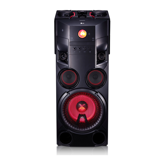
- Page 1 Internal Use Only Mini Hi-Fi AUDIO SERVICE MANUAL MODEL: OM7560 CAUTION BEFORE SERVICING THE UNIT, READ THE “SAFETY PRECAUTIONS” IN THIS MANUAL. P/NO : AFN77483239 APRIL, 2016...
- Page 2 CONTENTS SECTION 1 ..GENERAL SECTION 2 ..CABINET & MAIN CHASSIS SECTION 3 ..ELECTRICAL SECTION 4 ..MECHANISM (DM19AC) SECTION 5 ..REPLACEMENT PARTS LIST...
-
Page 3: Table Of Contents
SECTION 1 SUMMARY CONTENTS SERVICING PRECAUTIONS ..........................1-3 ESD PRECAUTIONS ............................1-5 HIDDEN KEY MODE ............................1-6 SERVICE INFORMATION FOR EEPROM ......................1-7 PROGRAM DOWNLOAD GUIDE ........................1-8 SPECIFICATIONS ............................1-11... -
Page 4: Servicing Precautions
SERVICING PRECAUTIONS NOTES REGARDING HANDLING OF THE PICK-UP 1. Notes for transport and storage 1) The pick-up should always be left in its conductive bag until immediately prior to use. 2) The pick-up should never be subjected to external pressure or impact. Storage in conductive bag Drop impact 2. - Page 5 NOTES REGARDING COMPACT DISC PLAYER REPAIRS 1. Preparations 1) Compact disc players incorporate a great many ICs as well as the pick-up (laser diode). These components are sensitive to, and easily affected by, static electricity. If such static electricity is high voltage, components can be damaged, and for that reason components should be handled with care.
-
Page 6: Esd Precautions
ESD PRECAUTIONS Electrostatically Sensitive Devices (ESD) Some semiconductor (solid state) devices can be damaged easily by static electricity. Such components commonly are called Electrostatically Sensitive Devices (ESD). Examples of typical ESD devices are integrated circuits and some field-effect transistors and semiconductor chip components. The following techniques should be used to help reduce the incidence of component damage caused by static electricity. -
Page 7: Hidden Key Mode
HIDDEN KEY MODE Push both Front key and RCU key to activate it for 5 seconds. 1. Disc Lock On/Off (CD Function Only Active) Front Key : STOP RCU Key :STOP 2. Check Version and Option code Front Key : STOP ... -
Page 8: Service Information For Eeprom
SERVICE INFORMATION FOR EEPROM POWER ON It is possible at any function. (ex. It is possible at VFD “NO USB” status, too.) VFD “NO DISC” status This is an example. Front ‘Stop’ + Remote control ‘ ’ push same timing during 5 s FLD “OP00-…..”... -
Page 9: Program Download Guide
PROGRAM DOWNLOAD GUIDE 1. AUDIO PROGRAM Download program file name must be MICOM_OM7560_YYMMDDX.HEX If security program(Water Wall) is activated on PC, you must save the file to the USB storage device and disable the security software, then download the file to your set. Downloading file proceeds in the same way at USB1 function and USB2 function. - Page 10 2. CD PROGRAM Download program file name must be HG690_OM7560_YYMMDDX.bin If security program(Water Wall) is activated on PC, you must save the file to the USB storage device and disable the security software, then download the file to your set. Downloading file proceeds in the same way at USB1 function and USB2 function.
- Page 11 3. EQ PROGRAM Download program file name must be EQ_PRG.BIN If security program(Water Wall) is activated on PC, you must save the file to the USB storage device and disable the security software, then download the file to your set. Downloading file proceeds in the same way at USB1 function and USB2 function.
-
Page 12: Specifications
SPECIFICATIONS • GENERAL Power requirements Refer to the main label. Power consumption Refer to the main label. Dimensions (W x H x D) 330 x 815 x 302 mm Net Weight (Approx.) 16.8 kg Operating temperature 5 °C to 35 °C (41 °F to 95 °F) Operating humidity 5 % to 90 % Bus Power Supply (USB) - Page 13 1-12...
- Page 14 SECTION 2 CABINET & MAIN CHASSIS CONTENTS DISASSEMBLY INSTRUCTIONS ........................2-2 EXPLODED VIEWS ............................2-3 1. CABINET AND MAIN FRAME SECTION ....................2-3 2. MECHANISM DECK SECTION (DM19AC) ....................2-5 3. PACKING ACCESSORY SECTION ......................2-7...
-
Page 15: Disassembly Instructions
DISASSEMBLY INSTRUCTIONS 1) When disassembling the Frame Top, do not rotate and disassemble by pulling upwards. Figure 1 2) To disassemble the Front Panel, remove the two screws and disassemble. Figure 2... -
Page 16: Exploded Views
EXPLODED VIEWS 1. CABINET AND MAIN FRAME SECTION NOTES) THE EXCLAMATION POINT WITHIN AN EQUILATERAL TRIANGLE IS INTENDED TO ALERT THE SERVICE PERSONNEL TO THE PRESENCE OF IMPORTANT SAFETY INFORMATION IN SERVICE LITERATURE. SMPS 260L MAIN CABLE4 260R CABLE1 CABLE2 CABLE3... -
Page 17: Mechanism Deck Section (Dm19Ac)
2. MECHANISM DECK SECTION (DM19AC) 1439 1002 A001 1005 1001 1026 1003 1004 1030 1437 1024 1437 1024 1024 1012 1049 1437 1013 1015 1024 1016 1020 1011 A006 1045 1019 1018 1043 A005 1439... -
Page 18: Packing Accessory Section
3. PACKING ACCESSORY SECTION Optional Part 808 Batteries 801 Owner’s manual 825 FM antenna 300 Power Cord 900 Remote control 803 Packing 803 Packing 804 Bag 802 Box... - Page 20 SECTION 3 ELECTRICAL CONTENTS ONE POINT REPAIR GUIDE ..........................3-2 1. NO POWER ............................3-2 2. NO BOOTING WHEN POWER ON THE SET..................3-3 3. VFD IS NOT DISPLAYED WHEN POWER ON THE SET ..............3-4 4. NO BOOTING (IN CD/USB FUNCTION) ....................3-5 5.
-
Page 21: One Point Repair Guide
ONE POINT REPAIR GUIDE 1. NO POWER If the unit doesn’t work by no power problem, repair the set according to the following guide. 1-1. FUSE/ THERMISTOR/ BRIDGE DIODE 1-1-1. Solution Please check and replace F901, TH901 or TH903, BD901 on SMPS board. 1-1-2. - Page 22 ONE POINT REPAIR GUIDE NO POWER If the unit doesn’t work by no PVDD problem, repair the set according to the following guide. 1-2. FUSE/ FET 1-2-1. Solution Please check and replace F901, Q901 on SMPS board. 1-2-2. How to troubleshoot (Countermeasure) 1) Check if the fuse F901 is open or short-circuit.
-
Page 23: No Booting When Power On The Set
ONE POINT REPAIR GUIDE 2. NO BOOTING WHEN POWER ON THE SET The set doesn’t work when press the power button on the top board or the remote control. 2-1. IC501 2-1-1. Solution Replace IC501 on MAIN board. 2-1-2. How to troubleshoot (Countermeasure) 1) Check the +12 VA (CN202) and 3.3VA (IC503) in standby mode. -
Page 24: Vfd Is Not Displayed When Power On The Set
ONE POINT REPAIR GUIDE 3. VFD IS NOT DISPLAYED WHEN POWER ON THE SET When power on the set, any icons or characters on VFD are not displayed. 3-1. VFD (VFD301) 3-1-1. Solution Please check and replace VFD301 on TOP FRONT board. 3-1-2. - Page 25 ONE POINT REPAIR GUIDE 4. NO BOOTING (IN CD/USB FUNCTION) After you turn on power key and displayed message in the following order (HELLO VOL XX CD or USB) on VFD, it will not display other message on VFD, and it will not boot-up normally. 4-1.
-
Page 26: No Booting (In Cd/Usb Function)
ONE POINT REPAIR GUIDE NO BOOTING (IN CD/USB FUNCTION) After you turn on power key and displayed message in the following order (HELLO VOL XX CD or USB) on VFD, it will not display other message on VFD, and it will not boot-up normally. 4-2. - Page 27 ONE POINT REPAIR GUIDE NO BOOTING (IN CD/USB FUNCTION) After you turn on power key and displayed message in the following order (HELLO VOL XX CD or USB) on VFD, it will not display other message on VFD, and it will not boot-up normally. 4-3.
- Page 28 ONE POINT REPAIR GUIDE 5. NO OPERATION OF MD When no sound output in the CD function, you can not listen to music reading data from a CD disc if the servo motors in MD don’t work. This step is for checking the SPINDLE MOTOR among them.
-
Page 29: No Operation Of Md
ONE POINT REPAIR GUIDE NO OPERATION OF MD When no sound output in the CD function, you can not listen to music reading data from a CD disc if the servo motors in MD don’t work. This step is for checking the SLED MOTOR among them. - Page 30 ONE POINT REPAIR GUIDE NO OPERATION OF MD When no sound output in the CD function, you can not listen to music reading data from a CD disc if the servo motors in MD don’t work. This step is for checking the TRAY OPEN / CLOSE MOTOR among them.
- Page 31 ONE POINT REPAIR GUIDE NO OPERATION OF MD When no sound output in the CD function, you can not listen to music reading data from a CD disc if the pickup module in MD doesn’t work. This step is for checking the LASER TRACKING ACTUATOR.
- Page 32 ONE POINT REPAIR GUIDE NO OPERATION OF MD When no sound output in the CD function, you can not listen to music reading data from a CD disc if the pickup module in MD doesn’t work. This step is for checking the LASER FOCUSING ACTUATOR.
- Page 33 ONE POINT REPAIR GUIDE 6. NO SOUND There is no sound output by DIGITAL AUDIO AMP DAMAGE, repair the set according to the following guide. 6-1. DIGITAL AUDIO AMP DAMAGE 6-1-1. Solution Replace IC701, IC702 on MAIN board. 6-1-2. How to troubleshoot (Countermeasure) 1) Check PWM_FL±, PWM_FR±...
-
Page 34: No Sound
ONE POINT REPAIR GUIDE NO SOUND There is no sound output in the CD FUNCTION, repair the set according to the following guide. 6-2. CD FUNCTION 6-2-1. Solution Replace IC501 on MAIN board. 6-2-2. How to troubleshoot (Countermeasure) 1) Check CD_BCK, CD_LRCK, & CD_DATA signals from IC501 to IC401. ... - Page 35 ONE POINT REPAIR GUIDE NO SOUND There is no sound output in the USB Function, repair the set according to the following guide. 6-3. USB FUNCTION 6-3-1. Solution Replace IC204 on MAIN board. 6-3-2. How to troubleshoot (Countermeasure) 1) Check +5V_USB to USB board. ...
- Page 36 ONE POINT REPAIR GUIDE NO SOUND There is no sound output in the AUX Function, repair the set according to the following guide. 6-4. AUX FUNCTION 6-4-1. Solution Replace IC201 on MAIN board. 6-4-2. How to troubleshoot (Countermeasure) 1) Check AUX_L/R signals to IC201 (pin23, 24). 2) Check if MCS_BCK, MCS_LRCK &...
- Page 37 ONE POINT REPAIR GUIDE NO SOUND There is no sound output in the TUNER function, repair the set according to the following guide. 6-5. TUNER FUNCTION 6-5-1. Solution Replace IC201 on MAIN board. 6-5-2. How to troubleshoot (Countermeasure) 1) Check if TUNER_LR is entered from pin1, 3 of TU500 to IC201 (pin26, 27). ...
- Page 38 ONE POINT REPAIR GUIDE NO SOUND There is no sound output in the PORTABLE Function, repair the set according to the following guide. 6-6. PORTABLE FUNCTION, 6-6-1. Solution Replace IC201 on MAIN board. 6-6-2. How to troubleshoot (Countermeasure) 1) Check if PT_LR signals to IC201 (pin9, 10). 2) Check if MCS_BCK, MCS_LRCK, &...
- Page 39 ONE POINT REPAIR GUIDE NO SOUND There is no sound output in the MIC IN function, repair the set according to the following guide. 6-7. MIC IN function 6-7-1. Solution Replace IC206 on MAIN board, ICA301 on TOP FRONT board. 6-7-2.
- Page 40 ONE POINT REPAIR GUIDE NO SOUND There is no sound output in the Bluetooth function, repair the set according to the following guide. 6-8. BLUETOOTH FUNCTION 6-8-1. Solution Replace IC501 on the MAIN board or bluetooth module on the FRONT Panel. 6-8-2.
-
Page 41: Electrical Troubleshooting Guide
ELECTRICAL TROUBLESHOOTING GUIDE 1. POWER (SMPS) No 12 VA F901 normal? Replace F901 (Use the same fuse). BD901 normal? Replace BD901. TH901(TH903) normal? Replace TH901. Is Vcc (10 V ~ 18 V) supplied to D902 normal? IC901 pin7? Check or replace D902. D933 normal? Replace D933. - Page 42 ELECTRICAL TROUBLESHOOTING GUIDE No PVDD F901 normal? Replace F901 (Use the same fuse). BD901 normal? Replace BD901. TH901(TH903) normal? Replace TH901. Is Vcc (10 V ~ 18 V) supplied to D903 normal? IC911 pin4? Check or replace D903. Q911 base HIGH? •...
- Page 43 ELECTRICAL TROUBLESHOOTING GUIDE No LED Is Vcc (DVCC_3.3V) Check or replace IC505 supplied to IC103? Is LED_5V & F_LED_12V is normal? Check or replace IC207, Q210 & Q209. Check or replace IC931. No VFD Check or replace Q209, Q210. VFD_12V is normal? DVCC_5V &...
-
Page 44: Mcs Part Check
ELECTRICAL TROUBLESHOOTING GUIDE 2. MCS PART CHECK MCS PART CHECK Check if voltage Refer to SMPS troubleshooting. of CN202 pin1, 2: 12 V. Check if IC205 Check and change IC205. have 3.3 VA & 1.2 VA output. Check if IC505 Check and change IC505. -
Page 45: Fld Display Check
ELECTRICAL TROUBLESHOOTING GUIDE 3. FLD DISPLAY CHECK FLD DISPLAY CHECK Check Refer to SMPS/MPEG CN202 pin1, 2: 12 V input troubleshooting. voltage. Check Check if both end voltage DVCC_5V(Q205 & Q204) of FL+, FL- are over 1.85 V VH : Q801, Q802, D801~D804. VH : over 29 V. -
Page 46: Pwm Modulation Check
ELECTRICAL TROUBLESHOOTING GUIDE 4. PWM MODULATION CHECK PWM MODULATION PART CHECK Check CN202 Refer to pin1, 2: 12 V. SMPS troubleshooting. • Check IC601(TAS5548) 3.3 V - pin9, 14, 35, 50. • Check X601 (12.288 MHz). Check Check X601 Replace X601(12.288 MHz). X601(12.288 MHz) (12.288 MHz). -
Page 47: Power Amp Part Check
ELECTRICAL TROUBLESHOOTING GUIDE 5. POWER AMP PART CHECK POWER AMP PART CHECK Check CN202 pin1, 2: 12 V, Refer to SMPS troubleshooting. pin8, 9, 10: 48.5 V (35.5 V). Check IC701, IC702 Pin51, 52, 42, 43, 38, 39, 30, 31 input voltage. Check IC701, IC702 Check each line resistor output voltage. -
Page 48: Tuner / Aux Function Check
ELECTRICAL TROUBLESHOOTING GUIDE 6. TUNER / AUX FUNCTION CHECK FUNCTION CHECK Check IC201 (CS5346) Check JK200, TU500. pin23, 24, 26, 27 input. Check IC201 Check IC201 Check CN202 pin1, 2: 12 V. (CS5346) pin41 output Pin5: DVCC_3.3V Pin14: DVCC_5V. data. Check Check IC201 Check IC201... -
Page 49: Tuner Function Check
ELECTRICAL TROUBLESHOOTING GUIDE 7. TUNER FUNCTION CHECK TUNER FUNCTION CHECK Check tuner module (TU500) Check tuner module voltage (pin4: DVCC_3.3V). operation. Check IC501 Pin P7, P8, P10, P11. Check tuner module data. Refer to function check. 3-30... -
Page 50: Cd Function Check
ELECTRICAL TROUBLESHOOTING GUIDE 8. CD FUNCTION CHECK CD FUNCTION Is motor_open/close ok? Can the Is load +,- ok? (IC400 pin6, 7) disc insert? Check IC400. Is motor ok? (about 12 Ω) Check loading motor. Check IC400 (Motor drive IC). Focus, IM driving Disc reading tracking, sled signal... -
Page 51: Double Usb Function
ELECTRICAL TROUBLESHOOTING GUIDE 9. DOUBLE USB FUNCTION USB FUNCTION Plug-in USB device. Check CN502. Check USB_5V. Display “NO USB”. Check USB_D+, D- Check USB jack Display “READ”. (R573, R574, C573, C574 (CN801, CN802). D501, D502). Check IC501 Display “NO FILE”. Replace IC501. -
Page 52: Waveforms Of Major Check Point
WAVEFORMS OF MAJOR CHECK POINT 1. DSP (IC501) X X I X X I Fig 1-1. X501: Crystal of RTC 32.768 MHz Fig 1-2. X500: Crystal of system 24 MHz (R5D6 both side) ( MAIN DSP : R508, C503 ) 3-33... -
Page 53: Sdram (Ic502)
2. SDRAM (IC502) Fig 2. SDRAM 3-34... -
Page 54: Servo (Ic401)
3. SERVO (IC401) X X I Fig 3-2. CD-16M Fig 3-1. X400: Crystal 16.9344 MHz (IC401 pin31) 3-35... -
Page 55: Motor Driver (Ic400)
4. MOTOR DRIVER (IC400) Fig 4-2. SL- & SL+ for Driving SPINDLE Motor Fig 4-1. LO- & LO+ / MOT_OPEN &MOT_CLOSE (IC400 Pin11, 12) for Driving TRAY Motor (IC400 Pin6, 7, 9, 10) Fig 4-3. SP- & SP+ for Driving SPINDLE Motor (IC400 Pin17, 18) 13 15 3-36... -
Page 56: Usb (Cn502)
5. ADC (IC201) 6. USB (CN502) Fig 5. ADC I2S Fig 6. USB D+/D- (IC201 Pin42, 43,44) (CN502 Pin1, 2, 8, 9) 3-37... -
Page 57: Bluetooth (Cn504)
7. BLUETOOTH (CN504) B B T_TX BT_TX BT_TX BT_RX BT_RX BT_RX BT_RST BT_RST BT_RST Fig 7. BT_TX / BT_RX / BT_RST 3-38... -
Page 58: Wiring Diagram
WIRING DIAGRAM Tuner AUX IN/OUT IC201 IC504 IC503 IC502 CS5346 5pin FL/FR F/S 1M F/S 16M SDRAM W25Q80 W25Q18 W9825G6KH IC501 MLC3730 IC401 RF IC L718 L705 BU9546 L707 L706 IC400 MAIN Board Motor DR AM5890 USB1 USB2 IC701 IC702 IC206 10pin 10pin... -
Page 59: Block Diagrams
BLOCK DIAGRAMS 1. SYSTEM BLOCK DIAGRAM [OM7560 : Total 1000W] WOOFER : 360W X 1CH FRONT : 320W X 2CH 3-41 3-42... -
Page 60: Power Block Diagram
2. POWER BLOCK DIAGRAM 300mA IC203 330mA BOOM B LED LED_5V 500mA SN1501019 USB1 USB_5V SMPS BD2242G [3A] 785mA 135mA 500mA [2.1] SPK LED USB2 60mA EXPENDER MOTO DRIVE 350mA Front LED AM5890 25mA 50mA LINE OUT CS5346 DRV632 11mA 11mA MIC ADC EXPENDER... -
Page 61: Audio Path Block Diagram
3. AUDIO PATH BLOCK DIAGRAM LINE PWM_ L_IN PWM_ R_IN DRV632 PWM – RCH PWM – LCH PWM – FLCH TAS5548 LRCK PWM –FRLCH TAS5631 PWM –WCH AUX_SDIN2 MIX_SDIN1 MCLK MIX_DATA0 IC201 AUX_DATA LRCK CS5346 33pF MLC3730 ADC_DATA_IN Main DSP CD_16M SERVO CD_BCK... -
Page 62: Circuit Voltage Chart
CIRCUIT VOLTAGE CHART 1. IC INPUT VOLTAGE 2. CAPACITOR VOLTAGE 110V/60Hz-10% 230V/50Hz+10% 88 V, 60 Hz 288 V, 60 Hz Locaton/ Parts Parts Name Specifi cation (V, mV) Location Voltage (V) Voltage (V) Voltage (V) Current (mV) Voltage (V) Current (mV) IC101 C231 4.95... - Page 63 3. CONNECTOR VOLTAGE Connector Connector Connector Location Pin No. Pin Name Voltage(V) Location Pin No. Pin Name Voltage(V) Location Pin No. Pin Name Voltage(V) Name Name Name 3.3VA 3.29 OPEN_SW 3.25 3.29 CLK_FORM UCOM 0.00 0.01 3.29 DAT_FORM UCOM 0.00 CLOSE_SW 3.25 CN601...
-
Page 64: Connector Voltage
CONNECTOR VOLTAGE Connector Connector Location Pin No. Pin Name Voltage(V) Location Pin No. Pin Name Voltage(V) Name Name 0.00 SPACE_EXP_DAT 3.11 0.07 SPACE_EXP_CLK 0.00 MAIN 0.07 0.00 CN801 USB1 (2.0) CN851 SPACE USB 5V 5.07 DVCC_3.3V 3.25 LIGHTING 0.00 DGND 0.00 0.00... -
Page 65: Printed Circuit Board Diagrams
PRINTED CIRCUIT BOARD DIAGRAMS 1. SMPS P.C.BOARD (TOP VIEW) (BOTTOM VIEW) NOTE) Warning Parts that are critical with respect to risk of fire or electrical shock. 3-75 3-76... -
Page 66: Main P.c.board
2. MAIN P.C.BOARD (TOP VIEW) 3-77 3-78... - Page 67 MAIN P.C.BOARD (BOTTOM VIEW) 3-79 3-80...
- Page 68 3. TOP FRONT P.C.BOARD (TOP VIEW) 3-81 3-82...
-
Page 69: Top Front P.c.board
TOP FRONT P.C.BOARD (BOTTOM VIEW) 3-83 3-84... -
Page 70: Jack/ Rmc P.c.board
4. JACK/ RMC P.C.BOARD (TOP VIEW) (BOTTOM VIEW) 5. FRONT LED P.C.BOARD (TOP VIEW) (BOTTOM VIEW) 3-85 3-86... - Page 71 SECTION 4 MECHANISM (DM19AC) CONTENTS DECK MECHANISM PARTS LOCATIONS • Top View ..............................4-2 • Top View(without Tray Disc) ........................4-2 • Bottom View .............................. 4-2 DECK MECHANISM PARTS LOCATIONS 1. Main Base ............................... 4-3 1-1. Clamp Assembly Disc ........................4-3 1-1-1.
-
Page 72: Deck Mechanism Parts Locations
DECK MECHANISM PARTS LOCATIONS • Top View Procedure Parts Fixing Type Fig. Disassembly Starting No. Main Base Clamp Assembly Disc 1, 2 Plate Clamp 1, 2, 3 Magnet Clamp 1, 2, 3, 4 Clamp Upper Tray Disc 1, 6 Base Assembly Sled 4 Screws, 1, 2, 6 Gear Feed... -
Page 73: Main Base
DECK MECHANISM DISASSEMBLY TRAY DISC MAIN BASE PLATE CLAMP MAGNET CLAMP BASE MAIN DISC CLAMP ASSEMBLY CLAMP UPPER (Fig. A) HOLDER LEVER BASE MAIN BOTTOM SIDE VIEW BASE MAIN Fig. 4-1 Fig. 4-2 Fig. 4-2 1. Main Base (Fig. 4-1) 2. -
Page 74: Base Assembly Sled
RUBBER DAMPER Distinguish upper and (S2) lower sides (Assemble with care) (S2) RUBBER DAMPER Distinguish upper and (S2) lower sides RUBBER DAMPER (Assemble with care) BASE PU (S2) RUBBER DAMPER GENERAL PICK UP ASSEMBLY GEAR RACK SPINDLE MOTOR ASSEMBLY Fig. 4-3 3. -
Page 75: Frame Assembly Up/Down
UP/DOWN FRAME ASSEMBLY BASE MAIN (L5) GUIDE UP/DOWN FIG. (A) GUIDE UP/DOWN GUIDE UP/DOWN GEAR LOADING GEAR PULLEY (L4) BASE MAIN BELT LOADING PWB ASSEMBLY LOADING (C2) (S5) Fig. 4-4 5. Frame Assembly Up/Down (Fig. 4-4) 8. Gear Loading (Fig. 4-4) Note 9. -
Page 76: Deck Mechanism Exploded View (Dm19Ac)
DECK MECHANISM EXPLODED VIEW (DM19AC) 1439 1002 A001 1005 1001 1026 1003 1004 1030 1437 1024 1437 1024 1024 1012 1049 1437 1015 1013 1024 1016 1020 1011 A006 1045 1019 1018 1043 A005 1439...