Yamaha A5000 Service Manual
Professional sampler
Hide thumbs
Also See for A5000:
- Owner's manual (296 pages) ,
- Supplementary manual (25 pages) ,
- Owner's manual (27 pages)
Table of Contents
SY 011491
A5000 19991210-229000
A4000 19991210-149000
PROFESSIONAL SAMPLER
SERVICE MANUAL
CONTENTS
SPECIFICATIONS ................................................................................ 3
PANEL LAYOUT .................................................................................. 4
CIRCUIT BOARD LAYOUT ................................................................... 5
BLOCK DIAGRAM ............................................................................... 6
DISASSEMBLY PROCEDURE ............................................................ 7
LSI PIN DESCRIPTION ...................................................................... 10
IC BLOCK DIAGRAM ......................................................................... 16
TEST PROGRAM ............................................................................. 19
MIDI DATA FORMAT .......................................................................... 32
MIDI IMPLEMENTATION CHART ........................................................ 43
HAMAMATSU,JAPAN
1.57K-859 I Printed in Japan2000.01
Table of Contents

Related Manuals for Yamaha A5000


Summary of Contents for Yamaha A5000
-
Page 1: Table Of Contents
IC BLOCK DIAGRAM ................. 16 TEST PROGRAM ................19 ERROR MASSAGE ................31 MIDI DATA FORMAT ................32 MIDI IMPLEMENTATION CHART ............43 PARTS LIST OVERALL CIRCUIT DIAGRAM CIRCUIT BOARDS SY 011491 HAMAMATSU,JAPAN A5000 19991210-229000 1.57K-859 I Printed in Japan2000.01 A4000 19991210-149000... -
Page 2: Important Notice
A5000/A4000 IMPORTANT NOTICE This manual has been provided for the use of authorized Yamaha Retailers and their service personnel. It has been assumed that basic service procedures inherent to the industry, and more specifically Yamaha Products, are already known and understood by the users, and have therefore not been restated. -
Page 3: Specifications
IDE Cable for Internal Hard Disk 6 minutes 20 seconds (44.1 kHz) Owner’s manual 12 minutes 40 seconds (22.05 kHz) Options (made by Yamaha) 25 minutes 21 seconds (11.025 kHz) AIEB1: I/O expansion board 50 minutes 43 seconds (5.5125 kHz) -
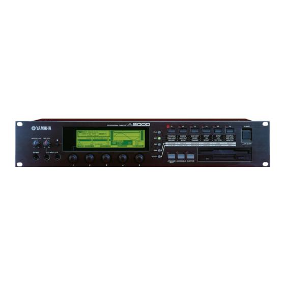
Page 4: Panel Layout
Audition button Floppy Disk Drive Power switch Rear Panel AC inlet Midi In-A, In-B, Out, Thru-A, Thru-B (A5000) connectors / Midi In, Out, Thru (A4000) connectors Assignable Out L, R jacks Stereo Out L/Mono, R jacks SCSI connector Optical In, Out connectors... -
Page 5: Circuit Board Layout
A5000/A4000 CIRCUIT BOARD LAYOUT... -
Page 6: Block Diagram
A5000/A4000 BLOCK DIAGRAM... -
Page 7: Disassembly Procedure
A5000/A4000 DISASSEMBLY PROCEDURE Top Cover Remove the sixteen (16) screws marked [510] and slide the Top Cover to the back side. The top cover can be then removed. (Fig.1) Circuit Boards and Unit After removing the top cover, remove the following screws. Each circuit board can then be removed. -
Page 8: Front Panel
A5000/A4000 (Fig.2) (Fig.3) Front Panel Remove the knob marked [440], [450], [460]. Remove the three (3) screws marked [410]. And remove the Front Panel from the Lower Case Assembly. (Fig.4) - Page 9 A5000/A4000 Circuit Boards and Unit After removing the front panel, remove the following screws. Each circuit board can then be removed.(Fig.5) Circuit Boards and Unit Ref.No. Screw [S230] Hexagonal Nut 14X2 M12 (ES200210) [L170] Bind Head Tapping-B 3.0X6 MFZN2Y (EP600130)
-
Page 10: Lsi Pin Description
A5000/A4000 LSI PIN DESCRIPTION TC203C760HF-002 (XS725A00) SWP30B (AW M Tone Generator coped with MEG) Standard W ave Processor (IC507) NAME FUN CTION NAME FUN CTION N O. N O. (Gr ound) (Gr ound) HMD0 HMD1 HMD2 HMD3 HMD4 Address bus of inter nal register... - Page 11 A5000/A4000 D65621GF-028-3B9 (XS370A00) SMI (IC516) NAME FUNCTION NAME FUNCTION LMA24 Power Supply LMA23 L1RAS2 RAS2 for LoMem SIMM 1 LMA22 L1RAS3 RAS3 for LoMem SIMM 1 LMA21 Low Memory Address Ground LMA20 HDRAS0 RAS for HiMem DRAM 0 LMA19 HDRAS1...
- Page 12 A5000/A4000 D65636GF-104-3B9 (XS369A00) SPF (IC11) NAME FUNCTION NAME FUNCTION Initial Clear SYNIO Serial Input0 Sync Clock(48kHz) Power Supply Power Supply Ground Ground Data Bus DIN0 Serial Input0 Data Input(1.6MHz) CK256I1 Serial Input1 256fs Clock(12.8MHz) Ground BCKI1 Serial Input1 Bit Clock(3.2MHz)
- Page 13 A5000/A4000 HD63266F (XI939A00) FDC (Floppy Disk Controller) (IC8) NAME FUNCTION NAME FUNCTION 8"//5" Data transmission speed /TRKO Track 00 signal XTALSET Clock select /INDEX Index signal /RESET Rest /RDATA Read data input from FDD E//RD Enable/Read XTAL2 Clock RW//WR Read/write/Write...
- Page 14 A5000/A4000 HD6437043AE00F (XW795A00) CPU (IC1) NAME FUNCTION NAME FUNCTION /WRHH HH write DACK0 DMA transfer strobe Data bus PA22 Port A /CASHH HH Column address strobe PE15 Port E Power supply Ground Data bus Ground Address bus Data bus Power supply...
- Page 15 A5000/A4000 MB87034PF (XK851A00) SPC (SCSI Protocol Controller) (IC52) NAME FUNCTION NAME FUNCTION /RESET Reset /CLK Clock Ground Ground /DBP SCSI data bus /I/O Data direction Ground Ground /DB7 /REQ Request /DB6 SCSI data bus /C/D Command/Data /DB5 /SEL Select Power supply...
-
Page 16: Ic Block Diagram
A5000/A4000 IC BLOCK DIAGRAM... - Page 17 A5000/A4000...
- Page 18 A5000/A4000...
-
Page 19: Test Program
A5000/A4000 TEST PROGRAM TEST No. TEST TEST RESULTS MIDI OK/NG ALL DOTS ON/OFF LED/SWITCH LIT, OK/NG ENCODER OK/NG CPU (DRAM/EEPROM/DPRAM) OK/NG WAVE MEMORY OK/NG SIMM Displayed CAPACITY/NG ADDRESS (SIMM) DRIVE 1SECTOR/DMA (SCSI) OK/NG DRIVE 1SECTOR (IDE) OK/NG FD INSERT/VERIFY OK/NG... - Page 20 The test program can be entered in either of the two ways. AUTO MANUAL 1.Turn on the A5000/A4000 power switch while pressing the [F1] and the [COMMAND] switches. The test is proceeded to use the [ENC4], [ENC5], [COMMAND] 2.After turning on the A5000/A4000 power switch, wait a few and [ASSIGNABLE].
- Page 21 MIDI cable is joined the following and the test will be executed. AUTO MANUAL MIDI-A-OUT === MIDI-A-IN (A4000,A5000) MIDI-A-THRU === MIDI-B-IN (A5000) NG : 02: LED/SW N G S W # : < * * * * * * > AUTO...
- Page 22 A5000/A4000 RESULT OF THE TEST CPU (DRAM/EEPROM/DPRAM/FLASH) OK : 04: C P U ( D R A M / E E P R O M / D P R A M / F L A S H ) 06: S I M M...
- Page 23 0 8 : D R I V E 1 S E C T O R ( I D E ) formated by A5000/A4000 or formated for MS-DOS. Be sure that D E S T R U C T I V E !
- Page 24 A5000/A4000 While sounding, the LCD shows as belows. RESULT OF THE TEST OK : Output on AUTO MANUAL NG : RESULT OF THE TEST N G S W P a c c e s s e r r o r...
- Page 25 A5000/A4000 When inserting in the REC IN-R RESULT OF THE TEST STEREO OUT-L: less than -55 dBm OK / NG STEREO OUT-R: 1 kHz +/- 1.5 Hz, sine wave, less than 3.0% distortion -1 +/- 4 dBm (10 k ohm load) END OF THE TEST After displaying the result, the test will be finished.
- Page 26 A5000/A4000 ASSIGNABLE OUT-5: 1 kHz +/- 1 Hz, sine wave, less than 0.5% ASSIGNABLE OUT-3 distortion 0 +/- 3 dBm (10 k ohm load) 20: ASSIGNABLE OUT-3 ASSIGNABLE OUT-6: less than -70 dBm (10 k ohm load) AUTO MANUAL Insert the appropriate phone plugs into the ASSIGNABLE OUT-3 While sounding, the LCD shows as below.
- Page 27 A5000/A4000 RESULT OF THE TEST DIGITAL IN 2 5 : D I G I TA L I N 2 6 : O P T I C A L I N AUTO MANUAL AUTO MANUAL Insert the appropriate phone plugs into the STEREO OUT-L termi- NG : nal.
- Page 28 A5000/A4000 6) When executing the mLAN clock test, the display is as below. RESULT OF THE TEST 2 7 : m L A N I / F ( 2 6 p i n ) OK : AUTO MANUAL U S I N G M L A N B O A R D C L O C K...
-
Page 29: Factory Set
SCSI TERM POWER Connect the DIGITAL IN terminal and the DIGITAL OUT terminal Turning on the A5000/A4000 power switch, test can start after more and execute the test. Check the test result on the LCD. than 5 seconds. The voltage can be measured the SCSI connector for... - Page 30 A5000/A4000 SCSI TERM SW Turning on the A5000/A4000 power switch, the test can start after more than 5 seconds. The voltage can be measured the SCSI connec- tor for the internal connect and the DM circuit board of the CN9-2 pin (the SCSI signal line).
-
Page 31: Error Messages
SIMM configuration error....... The A5000/A4000 was not able to start up, due to the fact that expansion SIMM’s are not installed in pairs, or because the usage order of the expansion slots is incorrect etc. -
Page 32: Midi Data Format
Program Change $F0,$7E,$nn,$06,$02 Identity Reply < SW > $Cn,$00 Program Change enable/disable (*1) For the A5000 one of the A/B inputs can be selected. $Cn,$7F < MIDI transmission conditions > After Touch < SW > $Dn After Touch Note Off... - Page 33 EF3 Parameter 1 - 16 0 - 127 2.1.6. Program changes 0-120 EF4 Level 0 - 127 * (A5000 only) 0-120 EF4 Pan 0 - 127 * (A5000 only) When a program change message is received, the corresponding program is selected for...
- Page 34 = Sustain loop end point (LSB first) Sample Dump Request is received. 0iiiiiii iiiiiii = The A5000/A4000 will automatically detect whether the MIDI connections are an open 0iiiiiii iiiiiii = loop or a closed loop, and will automatically switch to use or not use hand shaking.
- Page 35 Software revision level $nnnn A5000/A4000 software version “PG” Program bulk dump (*1) For the A5000 the range is $01DB, and the content is #0475. “SB” Sample bank bulk dump “SP” Sample bulk dump This message is only transmitted in response to an Identity Request message.
- Page 36 A5000/A4000 5.3.1. Parameter change (object select) 5.3.5. Parameter request (object) 01110000 11110000 01000011 01000011 0001nnnn nnnn = Device Number 0011nnnn nnnn = Device Number 01011000 $58 g=22,h=0 01011000 $58 g=22,h=0 00000000 00000001 0ccccccc 0ppppppp parameter number P1-P6 (6byte) object name (ASCII 16byte)
- Page 37 9byte — reserved 0408 56*n byte [Easy Edit Parameter]*(number of samples) (*1) Number of samples/sample banks for which ToPgm is on. (*2) -2:off, -1:AUDITION, 0-15:A01-16, 16:basic receive channel, 17-32:B01-16(A5000 only) (*3) -1:all (*4) Refer to *8 of “2.1.1 Program Parameters”.
- Page 38 PEG sustain level (*2) -1:”=sample” (*3) Each bn and bn+1 is 1:”=sample”. 0143 +/-127 PEG release level (*4) -1:”=sample”, 0-15:A01-A16, 16:basic receive channel, 17-32:B01-16(A5000 only) 0144 +/-7 PEG rate key scaling (*5) -1:”=sample”, Refer to *8 of “2.1.1 Program Parameters”.
- Page 39 0456 loop remix zone start point b0:MIDI channel B01 controller reset... 0457 loop remix zone end point ( >start) b15:MIDI channel B16 controller reset (A5000 only) 0458 assignable L&R output level offset 1502 b0:MIDI channel B01 note on normal/toggle... 0459 assignable 1&2 output level offset...
- Page 40 Easy Edit Parameters (*5) -1:”=Orig” P2 x 100 + P3 is the number of the sample (bank) assigned to the program. (*6) -2:off, -1:AUDITION, 0-15:A01-A16, 16:basic receive channel, 17-32:B01-16 (A5000 only) P3 = 0-98 only when P2 = 9. (*7) -1:all 0-99 —...
- Page 41 +/-63,64-68 Q/width velocity sensitivity (*4) program control4 range — — — — UC fixed pitch on — — — — SC +/-7 detune effect4-parameter1 (A5000 only) — — — — SC +/-63 dephase (A5000 only) — — — — SC +/-63 expand width...
- Page 42 MIDI basic channel omni on (*4) 64-68:”Rnd1"-”Rnd5" — — — MIDI program change (*5) 1: depends on any sample bank. receive enable (*6) 0-15:A01-16, 16:basic receive channel, 17-32:B01-16 (A5000 only) — — -1,0-32 knob2-5 control MIDI transmit (*7) channel (*1) value filter type —...
-
Page 43: Midi Implementation Chart
A5000/A4000 MIDI IMPLEMENTATION CHART... -
Page 44: Parts List
A5000/A4000 PARTS LIST CONTENTS OVERALL ASSEMBLY ......... 2 ELECTRICAL PARTS ........... 5 Note) DESTINATION ABBREVIATIONS Australian model South African model British model Chinese model Canadian model South-east Asia model German model Taiwan model European model U.S.A. model French model General export model (110V) - Page 45 A5000/A4000 OVERALL ASSEMBLY...
- Page 46 Front Panel Assembly A4000 EP600130 Bind Head Tapping Screw-B 3.0X6 MFZN2Y VM825700 Mode Button PLAY,EDIT,REC,DISK,UTILITY VF888700 Push Rod POWER ON/OFF VU931600 Knob ENCODER A5000 1,2,3,4,5 V5424000 Knob ENCODER A4000 1,2,3,4,5 VP826500 Knob (small) REC VOLUME VP826800 Knob (small) MASTER VOLUME V4717100...
- Page 47 A5000/A4000 DESCRIPTION REMARKS PART NO. QTY RANK REF NO. Circuit Board Assembly E, B (V481230) V3612600 Power Supply Unit J, U V3612700 Power Supply Unit E, B V4537900 Connector Assembly ACIN-PS VL785200 P20a AC-IN Connector AC-P01CR02 CB069250 Cord Holder BK-1...
-
Page 48: Electrical Parts
A5000/A4000 ELECTRICAL PARTS DESCRIPTION REMARKS PART NO. QTY RANK REF NO. ELECTRICAL PARTS A5000,A4000 V4312000 A5000 (XW129C0) Circuit Board V4312100 Circuit Board A4000 (XW129C0) V4457300 Circuit Board (XW531B0) VV331600 Circuit Board (XS547A0) V4457200 Circuit Board (XW473B0) V4457400 Circuit Board (XW573B0) - Page 49 A5000/A4000 DESCRIPTION REMARKS PART NO. QTY RANK REF NO. XR337A00 IC42 TC74VHC32F-TEL XR337A00 IC43 TC74VHC32F-TEL XN883A00 IC44 TC7W14FU INVERTER XT812A00 IC45 TC74VHC11F(EL) INVERTER XR337A00 IC46 TC74VHC32F-TEL XY363A00 IC49 TC7WH04FU INVERTER XW948A00 IC50 TC7WH08FU XH223A00 IC51 SN74HC273NSR D-FF XK851A00 IC52 MB87034PF...
- Page 50 A5000/A4000 DESCRIPTION REMARKS PART NO. QTY RANK REF NO. XS534A00 IC815 NJM78M05DLA REGULATOR +5V XS775A00 INVERTER IC816 TC7SH04FU XT487A00 IC821 TC74VHC245F TRANSCEIVER XW357A00 IC822 DS90C402M LINE RECEIVER XY618A00 IC823 TC7SH32F VG518300 Jumper Header 2P TE VG518300 J100 Jumper Header 2P TE...
- Page 51 A5000/A4000 DESCRIPTION REMARKS PART NO. QTY RANK REF NO. UU167470 Electrolytic Cap.-FW 47.00 50.0V C:801,802,807,808,831,832,842 843,851,852,860,861,868,869 889,890,902,906 VV546700 Tantalum Capacitor (chip) 47 10V M C:613,614 VY844800 Capacitor (chip) C:856,872 UE046470 Electrolytic Cap. (chip) 4.7 25V RV2 C:62 UE066100 Electrolytic Cap. (chip)
- Page 52 A5000/A4000 DESCRIPTION REMARKS PART NO. QTY RANK REF NO. RD255220 R:6,8-15,162 Carbon Resistor (chip) 220.0 0.1 J RD255510 Carbon Resistor (chip) 510.0 0.1 J R:67 RD255560 Carbon Resistor (chip) 560.0 0.1 J R:28-32 RD256100 Carbon Resistor (chip) 1.0K 0.1 J...
- Page 53 A5000/A4000 DESCRIPTION REMARKS PART NO. QTY RANK REF NO. XV411A00 IC14 W24258S-70LE-EL10 SRAM 256K VN686000 IC15 Photo Coupler PC410T XL122A00 IC17 PST572CMT-R SYSTEM RESET XT015A00 IC20 TC74VHC138F DECODER XT015A00 IC21 TC74VHC138F DECODER XH225A00 IC22 SN74HC574NSR D-FF XH225A00 IC23 SN74HC574NSR D-FF...
- Page 54 A5000/A4000 DESCRIPTION REMARKS PART NO. QTY RANK REF NO. XQ138A00 IC810 NJM4556AMT1 OP AMP XR339A00 IC811 TC9246F-TEL XT487A00 IC812 TC74VHC245F TRANSCEIVER XT487A00 -814 TC74VHC245F TRANSCEIVER XS534A00 IC815 NJM78M05DLA REGULATOR +5V XS775A00 IC816 TC7SH04FU INVERTER XT487A00 IC821 TC74VHC245F TRANSCEIVER XW357A00 IC822...
- Page 55 A5000/A4000 DESCRIPTION REMARKS PART NO. QTY RANK REF NO. UE066100 Electrolytic Cap. (chip) 1 50V RV2 C:105 UF027220 Electrolytic Cap. (chip) 22 10V C:839,840 UF027330 Electrolytic Cap. (chip) 33 10V C:812,813,821,823,824,826 UF027470 Electrolytic Cap. (chip) 47 10V C:35,36 UF028100 Electrolytic Cap. (chip)
- Page 56 A5000/A4000 DESCRIPTION REMARKS PART NO. QTY RANK REF NO. 190,194,197,202,219,244 245,247,507,514,515,519,520 526,527,566-573,801,805,809 821,829-831,858-861,868,869 880-882,887,891-893,954,955 960,961,977 RD257470 Carbon Resistor (chip) 47.0K 0.1 J R:804 RD258100 Carbon Resistor (chip) 100.0K 0.1 J R:808,828,889,890,971,972 RD258220 Carbon Resistor (chip) 220.0K 0.1 J R:870,888 V4808300 Carbon Resistor (chip) 1.0K 1/2 J...
- Page 57 A5000/A4000 DESCRIPTION REMARKS PART NO. QTY RANK REF NO. VT119800 AC Cord J 7A 125V 3P 2.5M VB927800 AC Cord VB928000 AC Cord VP204400 AC Cord BS 3P V3075300 Floppy Disk Drive MF355F-3252MG F V 4 7 7 3 0 0...
-
Page 58: Overall Circuit Diagram
A5000/A4000 OVERALL CIRCUIT DIAGRAM 1/ 3 (DM 1/ 2) : Mylar Capacitor : Ceramic Capacitor : Tantalum Capacitor Note : See parts list for details of circuit board component parts. 28CC1-8815101 A5000/A4000 A5000/A4000... - Page 59 A5000/A4000 OVERALL CIRCUIT DIAGRAM 2/ 3 (DM 2/ 2) : Mylar Capacitor : Ceramic Capacitor : Tantalum Capacitor Note : See parts list for details of circuit board component parts. 28CC1-8815101 A5000/A4000 A5000/A4000...
- Page 60 A5000/A4000 OVERALL CIRCUIT DIAGRAM 3/ 3 (JK, RE, VR) : Mylar Capacitor : Ceramic Capacitor : Tantalum Capacitor Note : See parts list for details of circuit board component parts. JK : 28CC1-8815102 RE : 28CC1-8815103 VR : 28CC1-8815104 A5000/A4000...
-
Page 61: Circuit Boards
A5000/A4000 CIRCUIT BOARDS PNA CIRCUIT BOARD PLAY EDIT RE CIRCUIT BOARD VR CIRCUIT BOARD JK CIRCUIT BOARD ENC 5 ENC 4 ENC 3 ENC 2 ENC 1 DISK UTILITY INPUT-R Component side COMMAND AUDITION / EXIT ASSIGNABLE INPUT-L PHONES MASTER...