Sony CFD-S01 Service Manual
Hide thumbs
Also See for CFD-S01:
- Operating instructions (3 pages) ,
- Specifications (2 pages) ,
- Specifications (21 pages)
Table of Contents
SERVICE MANUAL
Ver. 1.3 2007.07
CD player section
System
Compact disc digital audio system
Laser diode properties
Emission duration: Continuous
Laser output: Less than 44.6 µW
(This output is the value measured at a distance of
about 200 mm from the objective lens surface on the
optical pick-up block with 7 mm aperture.)
Number of channels
2
Frequency response
20 - 20 000 Hz +1/–2 dB
Wow and flutter
Below measurable limit
Radio section
Frequency range
FM: 87.5 - 108 MHz
CND, E92, MX model:
AM: 530 - 1 710 kHz
TW model:
AM: 531 - 1 611 kHz
EXCEPT CND, E92, MX, TW model:
AM:531 - 1 611 kHz (9 kHz step)
530 - 1 610 kHz (10 kHz step)
IF
FM: 10.7 MHz
AM: 450 kHz
Antennas
FM: Telescopic antenna
AM: Built-in ferrite bar antenna
Sony Corporation
9-879-945-04
Personal Audio Division
2007G04-1
Published by Sony Techno Create Corporation
© 2007.07
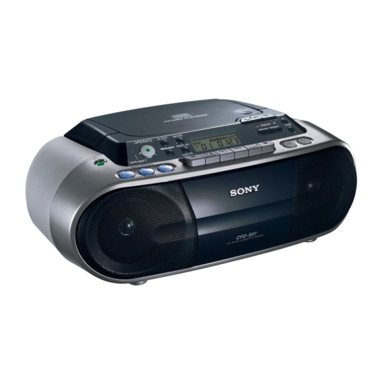
CFD-S01
Model Name Using Similar Mechanism CFD-S350L
CD
CD Mechanism Type
Section
Optical Pick-up Name
Model Name Using Similar Mechanism NEW
TC
Section Tape Transport Mechanism Type
SPECIFICATIONS
Cassette-corder section
Recording system
4-track 2 channel stereo
Fast winding time
Approx. 150 s (sec.) with Sony cassette C-60
Frequency response
TYPE I (normal): 80 - 10 000 Hz
General
Speaker
Full range: 8 cm dia., 4 Ω, cone type (2)
Outputs
Headphones jack (stereo minijack):
For 16 - 32 Ω impedance headphones
Power output
1.7 W + 1.7 W (at 4 Ω, 10% harmonic distortion)
Power requirements
For CD radio cassette-corder:
120 V AC, 60 Hz (CND, E92, MX, TW model)
230 V AC, 50 Hz (AEP, UK, E41, AUS, CET, IT, SP, TH model)
220 V AC, 60 Hz (KR model)
220 - 230 V AC, 50 Hz (AR model)
9 V DC, 6 R14 (size C) batteries
Power consumption
AC 13 W (CND, E92, MX, TW model)
AC 11 W (EXCEPT CND, E92, MX, TW model)
CD RADIO CASSETTE-CORDER
Canadian Model
AEP Model
UK Model
E Model
Australian Model
KSM-213CDP
KSS-213C
MF-S01
– Continued on next page –
Table of Contents

Related Manuals for Sony CFD-S01


Summary of Contents for Sony CFD-S01
- Page 1 4-track 2 channel stereo Laser diode properties Fast winding time Emission duration: Continuous Approx. 150 s (sec.) with Sony cassette C-60 Laser output: Less than 44.6 µW Frequency response (This output is the value measured at a distance of TYPE I (normal): 80 - 10 000 Hz about 200 mm from the objective lens surface on the optical pick-up block with 7 mm aperture.)
- Page 2 LES COMPOSANTS IDENTIFIÉS PAR UNE MARQUE 0 SUR LES DIAGRAMMES SCHÉMATIQUES ET LA LISTE DES PIÈCES SONT CRITIQUES POUR LA SÉCURITÉ DE FONCTIONNEMENT. NE REMPLACER CES COMPOSANTS QUE PAR DES PIÈCES SONY DONT LES NUMÉROS SONT DONNÉS DANS CE MANUEL OU DANS LES SUPPLÉMENTS PUBLIÉS PAR SONY.
-
Page 3: Table Of Contents
CFD-S01 Ver. 1.1 • UNLEADED SOLDER TABLE OF CONTENTS Boards requiring use of unleaded solder are printed with the lead- free mark (LF) indicating the solder contains no lead. SERVICING NOTES ..........4 (Caution: Some printed circuit boards may not come printed with the lead free mark due to their particular size.) -
Page 4: Servicing Notes
CFD-S01 SECTION 1 SERVICING NOTES LASER DIODE AND FOCUS SEARCH OPERATION CHUCK PLATE JIG ON REPAIRING CHECK On repairing CD section, playing a disc without the lid (CD), use 1. Turn ON the [OPERATE] button and press [CD] button to CD Chuck Plate Jig. -
Page 5: General
CFD-S01 SECTION 2 GENERAL This section is extracted from instruction manual. Basic Operations Selecting the play mode Presetting radio stations Press MODE until “ 1”, “ ”, “SHUF”, “SHUF” You can store radio stations into the player’s memory. and “ ”, “PGM”, or “PGM” and “ ” appear in You can preset up to 30 radio stations, 20 for FM and 10 the display. -
Page 6: Disassembly
CFD-S01 Ver. 1.1 SECTION 3 DISASSEMBLY Note: This set can be disassemble according to the following sequence. 3-1. CABINET (REAR) ASSY (Page 7) 3-2. CABINET (FRONT) ASSY, 3-12. POWER BOARD CABINET (UPPER) ASSY (Page 12) (Page 7) 3-3. MAIN BOARD 3-9. -
Page 7: Cabinet (Rear) Assy
CFD-S01 Note: Follow the disassembly procedure in the numerical order given. 3-1. CABINET (REAR) ASSY 2 screw (+BV tapping B2.6) 1 two screws telescopic antenna (+BV tapping (B2.6)) 4 three screws (+BV tapping (B2.6)) handle 3 screw (+BV tapping B2.6) -
Page 8: Main Board
CFD-S01 3-3. MAIN BOARD 1 CN306 (4P) 3 flexible flat cable (12 core) (CN802) 8 flexible flat cable (6 core) 2 flexible flat cable (14 core) (CN702) (CN801) 0 connector (S801) qa MAIN board 9 flexible flat cable (16 core) -
Page 9: Cd Motor Board
CFD-S01 3-5. CD MOTOR BOARD 3 CD MOTOR board 2 Remove the two solders. 1 Remove the two solders. 3-6. OPTICAL PICK-UP 5 optical pick-up 1 gear (A) claw 2 claw 4 sled shaft... -
Page 10: Control Board
CFD-S01 3-7. CONTROL BOARD 3 CONTROL board 2 five screws (+P tapping (B2.6)) 1 four screws (+P tapping (B2.6)) 3-8. CD LID 5 CD lid 6 CD spring... -
Page 11: Tape Mechanism Block, Belt (1), Belt (2)
CFD-S01 Ver. 1.1 3-9. TAPE MECHANISM BLOCK, BELT (1), BELT (2) 6 belt (1) 5 motor bracket 7 belt (2) 1 two screws (+BV tapping (B2.6)) 4 two screws 3 tape mechanism block 2 two screws (+BV tapping (B2.6)) 3-10. TC BOARD 2 Remove the four solders. -
Page 12: Key (Func) Board, Key (Vol) Board
CFD-S01 3-11. KEY (FUNC) BOARD, KEY (VOL) BOARD 9 button (FUNC) 6 three screws (+BV tapping (B2.6)) 8 KEY (FUNC) board 7 HOLD board 2 two screws (+BV tapping (B2.6)) 3 two HOLD boards 5 button (volume) 1 flexible flat cable (4 core) -
Page 13: Mechanical Adjustments
CFD-S01 SECTION 4 SECTION 5 MECHANICAL ADJUSTMENTS ELECTRICAL ADJUSTMENTS PRECAUTION TAPE SECTION 0 dB = 0.775 V 1. Clean the following parts with a denatured-alcohol-moistened swab : • Standard Output Level record/playback head pinch roller Output terminal HP OUT erase head... -
Page 14: Tuner Section
CFD-S01 Ver. 1.2 0 dB = 1 µV TUNER SECTION AM IF ADJUSTMENT Adjust for a maximum reading on level meter. • AM Section Setting: RADIO BAND•AUTO PRESET button: AM 450 kHz AM RF signal AM FREQUENCY COVERAGE CHECK (CND, E92, MX) - Page 15 CFD-S01 Adjustment Location: L3: AM FREQUENCY COVERAGE ADJUSTMENT CT1: FM TRACKING ADJUSTMENT L2: FM FREQUENCY COVERAGE ADJUSTMENT – MAIN BOARD (Component Side) – ANT1: AM TRACKING ADJUSTMENT CN701 CN702 CT3: AM TRACKING ADJUSTMENT L6: FM IF ADJUSTMENT L1: FM TRACKING ADJUSTMENT...
-
Page 16: Cd Section
CFD-S01 CD SECTION CD section adjustments are done automatically in this set. In case of operation check, confirm that focus bias. Test Point: FOCUS BIAS CHECK 1. Connect the oscilloscope between IC701 pin ts and pin 4 (or – MAIN BOARD (Conductor Side) –... -
Page 17: Diagrams
CFD-S01 SECTION 6 DIAGRAMS 6-1. BLOCK DIAGRAM — CD SECTION — LDACO (O) CD_IN_ L DIGITAL AC (I) SYNCHRONOUS (Page 18) FILTER CIRCUIT & CD_IN_R 1-bit DAC BD (I) PRI- SERVO RF AMP, E (I) SYSTEM SERVO PROCESSOR, DIGITAL SIGNAL PROCESSOR... -
Page 18: Block Diagram - Main Section
CFD-S01 6-2. BLOCK DIAGRAM — MAIN SECTION — IC302 R.RO ELECTRONIC VOLUME R.IN R.LIN POWER AMP REC/PB CD_IN_R IC303 PRE AMP R-CH (Page 17) L.RO IC301 VOL AMP J321 ALC 2 L-IN L-OUT L.LIN L.LO CD_IN_L HRP301 RECORD/PLAYBACK HEAD L.IN... -
Page 19: Circuit Boards Location
CFD-S01 Ver. 1.2 • NOTE FOR PRINTED WIRING BOARDS AND SCHEMATIC DIAGRAMS 6-3. CIRCUIT BOARDS LOCATION THIS NOTE IS COMMON FOR PRINTED WIRING BOARDS AND SCHEMATIC DIAGRAMS. POWER board (In addition to this, the necessary note is HEADPHONE board CD MOTOR board printed in each block.) -
Page 20: Schematic Diagram - Main Section (1/4)
CFD-S01 6-4. SCHEMATIC DIAGRAM — MAIN SECTION (1/4) — • Refer to page 19 for Waveforms. • Refer to page 32 for IC Block Diagram. • Refer to page 34 for IC Pin Description of IC701. R746 Q703 R742 R739... -
Page 21: Schematic Diagram - Main Section (2/4)
CFD-S01 Ver. 1.2 6-5. SCHEMATIC DIAGRAM — MAIN SECTION (2/4) — • Refer to page 19 for Waveforms. • Refer to page 31 for IC Block Diagram. IC B/D ANT1 ANT2 (Page 22) CND,E92,MX MODEL (EXCEPT CND,E92,MX MODEL) (EXCEPT CND,E92,MX MODEL) -
Page 22: Schematic Diagram - Main Section (3/4)
CFD-S01 Ver. 1.2 6-6. SCHEMATIC DIAGRAM — MAIN SECTION (3/4) — • Refer to page 19 for Waveforms. • Refer to page 36 for IC Pin Description of IC801. CN801 R844 R807 R847 IC805 R846 R848 IC804 R895 R896 R901... -
Page 23: Schematic Diagram - Main Section (4/4)
CFD-S01 Ver. 1.2 6-7. SCHEMATIC DIAGRAM — MAIN SECTION (4/4) — • Refer to page 32 for IC Block Diagrams. D323 C323 R323 R324 C324 R245 R145 C115 C113 R134 C129 C132 C130 R140 C110 R146 R148 R135 R136 C216... -
Page 24: Printed Wiring Board - Main Section
CFD-S01 Ver. 1.2 6-8. PRINTED WIRING BOARD — MAIN SECTION — • Refer to page 19 for Circuit Boards Location. : Uses unleaded solder. (Page 29) ANT2 FM TERESCOPIC POWER BOARD (Page 27) ANTENNA CN901 HEADPHONE BOARD CN307 C951 JW232... -
Page 25: Printed Wiring Boards - Tc Section
CFD-S01 6-9. PRINTED WIRING BOARDS — TC SECTION — • Refer to page 19 for Circuit Boards Location. : Uses unleaded solder. S701 (LIMIT) M702 R108 (SLED MOTOR) R110 R202 R314 R109 R305 R103 C101 R315 R104 M701 FFC020 R106... -
Page 26: Schematic Diagram - Tc Section
CFD-S01 Ver. 1.2 6-10. SCHEMATIC DIAGRAM — TC SECTION — • Refer to page 19 for Waveforms. • Refer to page 33 for IC Block Diagram. IC B/D IC301 C102 R102 R108 R103 R104 R112 R109 C301 C104 C103 R301... -
Page 27: Printed Wiring Boards - Control Section
CFD-S01 6-11. PRINTED WIRING BOARDS — CONTROL SECTION — • Refer to page 19 for Circuit Boards Location. : Uses unleaded solder. (Page 24) (Page 24) MAIN BOARD MAIN BOARD CN801 CN802 D406 CN402 OPR/BATT S403 MODE SLEEP S404 D406... -
Page 28: Schematic Diagram - Control Section
CFD-S01 6-12. SCHEMATIC DIAGRAM — CONTROL SECTION — R418 R419 R435 R436 R432 FFC090 FFC085 CN401 S416 S418 S405 S402 S415 JC401 S401 S410 S411 S412 S404 S403 CN402 R413 R424 R426 R428 R429 R430 R406 R403 R404 R409 R410... -
Page 29: Printed Wiring Boards - Power Supply Section
CFD-S01 6-13. PRINTED WIRING BOARDS — POWER SUPPLY SECTION — • Refer to page 19 for Circuit Boards Location. : Uses unleaded solder. FH901 FH902 F902 T901 C903 (11) 1-868-796- D903 C901 D901 MAIN BOARD C902 CN903 CN305 (Page 24) -
Page 30: Schematic Diagram - Power Supply Section
CFD-S01 6-14. SCHEMATIC DIAGRAM — POWER SUPPLY SECTION — CN902 CN903 C901 D901 D902 C902 CN901 T901 C903 F902 C906 D903 J901 D904 FH901 FH902 (Page 23) C904 CFD-S01... -
Page 31: Ic Block Diagrams
CFD-S01 • IC BLOCK DIAGRAMS IC1 LV23003VA (MAIN Board (2/4)) 36 FM RF-IN AM RF-IN 35 GND2 34 FM RF-OUT 33 VCC2 FM MIX 32 FM OSC GND1 AM MIX-OUT 31 AM OSC VCC1 30 BO2 29 BO1 BUFFER LOW-PASS... - Page 32 CFD-S01 IC703 BA5826FP-E2 (MAIN Board (1/4)) SP– D.BUFF D.BUFF LEVEL D.BUFF SL– SHIFT D.BUFF SPIN LEVEL SHIFT SLIN THERMAL SHUT-DOWN MONITOR (SLIN) REG–B VREF REGO MUTE (FIN) DRIVER MUTE (TIN) LEVEL LEVEL SHIFT D.BUFF SHIFT D.BUFF F– T– D.BUFF D.BUFF...
- Page 33 CFD-S01 IC302 PT2257-S (MAIN Board (4/4)) L-IN L-OUT VR 2 VOL AMP 2 VREF LOGIC CONTROL VOL AMP 1 REF AMP VR 1 R-IN R-OUT DATA IC301 TA2068N (TC Board) LINE L.LIN L.PO MIC I/EX AMP1 BUF AMP TAPE L.NF RADIO L.RAD...
- Page 34 CFD-S01 • IC PIN DESCRIPTIONS • IC701 BU9532KS2 (RF AMP, SYSTEM SERVO PROCESSOR, DIGITAL SIGNAL PROCESSOR) (MAIN BOARD (1/4)) Pin No. Pin Name Pin Description AVDD1 Power supply pin (+3.3V) AC (I) A+C RF signal input BD (I) B+D RF signal input...
- Page 35 CFD-S01 Pin No. Pin Name Pin Description TEN (O) Tracking error input CACG (O) RFAGC time constant capacitor fitted RFI (I) RF capacitor fitted EQO (O) RF EQ output...
- Page 36 CFD-S01 • IC801 µPD78947GC-A49-8BT-A (SYSTEM CONTROL) (MAIN BOARD (3/4)) Pin No. Pin Name Pin Description 1, 2 Not used. (Open) 3 to 5 VLC2 to 0 LCD drive bias voltage input 6 to 9 COM1 to 4 LCD drive common output...
- Page 37 CFD-S01 Pin No. Pin Name Pin Description Main system oscillation input (4.19 MHz) Main system oscillation output (4.19 MHz) System reset input V-CLK Volume command transfer clock output V-DATA Volume command data output SCULL EEPROM serial clock output EEPROM serial data input/output...
-
Page 38: Exploded Views
CFD-S01 Ver. 1.2 SECTION 7 EXPLODED VIEWS NOTE: • The mechanical parts with no reference • Accessories are given in the last of this parts list. The components identified by mark 0 or dotted line with mark. number in the exploded views are not supplied. -
Page 39: Front Cabinet Section (1)
CFD-S01 Ver. 1.2 7-2. FRONT CABINET SECTION (1) not supplied not supplied Ref. No. Part No. Description Remark Ref. No. Part No. Description Remark 3-252-827-01 SCREW (B2.6), (+) BV TAPPING 2-654-044-01 BUTTON (FF) (GRAY)...(GRAY) 2-655-159-01 JOINT, CABINET 2-654-044-11 BUTTON (FF) (GRAY)...(SILVER) 3-047-468-01 DAMPER 2-654-042-01 BUTTON (PLAY) (GRAY)...(GRAY) -
Page 40: Front Cabinet Section (2)
CFD-S01 Ver. 1.2 7-3. FRONT CABINET SECTION (2) SP201 SP101 Ref. No. Part No. Description Remark Ref. No. Part No. Description Remark A-1147-581-A KEY (FUNC) BOARD, COMPLETE X-2102-579-1 CABINET (FRONT) SUB ASSY 3-831-441-99 SHEET (1) (GUN METALLIC)...(GRAY) 1-831-616-11 CABLE, FLEXIBLE FLAT (4 CORE) -
Page 41: Upper Cabinet Section (1)
CFD-S01 Ver. 1.2 7-4. UPPER CABINET SECTION (1) S801 Ref. No. Part No. Description Remark Ref. No. Part No. Description Remark 2-654-053-01 LID, CD (DARK BLUE)...(GRAY) 3-252-827-01 SCREW (B2.6), (+) BV TAPPING 2-654-053-11 LID, CD (GRAY)...(SILVER) A-1147-588-A MAIN BOARD, COMPLETE... -
Page 42: Upper Cabinet Section (2)
CFD-S01 Ver. 1.2 7-5. UPPER CABINET SECTION (2) LCD401 Ref. No. Part No. Description Remark Ref. No. Part No. Description Remark 3-923-736-01 COVER, CD 1-831-617-11 CABLE, FLEXIBLE FLAT (14 CORE) 3-931-379-21 RUBBER, VIBRATION PROOF (RED) 3-831-441-99 SHEET (1) 3-931-379-31 RUBBER, VIBRATION PROOF (GREEN) -
Page 43: Cd Mechanism Section
CFD-S01 7-6. CD MECHANISM SECTION (KSM-213CDP) not supplied not supplied (M701 (SPINDLE)) M702 Ref. No. Part No. Description Remark Ref. No. Part No. Description Remark 2-626-907-11 GEAR (A) X-2162-709-2 CHASSIS ASSY (CDP), MOTOR (SPINDLE) 2-627-003-01 GEAR (B) (RP) (including M701) -
Page 44: Electrical Parts List
CFD-S01 Ver. 1.2 SECTION 8 BATTERY TERMINAL (F) ELECTRICAL PARTS LIST BATTERY TERMINAL (R) CD MOTOR CONTROL HEADPHONE NOTE: • Due to standardization, replacements in • COILS The components identified by uH : µH mark 0 or dotted line with mark. - Page 45 CFD-S01 Ver. 1.2 HEADPHONE KEY (FUNC) KEY (VOL) MAIN Ref. No. Part No. Description Remark Ref. No. Part No. Description Remark < RESISTOR > 1-165-176-11 CERAMIC CHIP 0.047uF 1-162-923-11 CERAMIC CHIP 47PF R146 1-216-809-11 METAL CHIP 1/10W (EXCEPT CND,E92,MX) R148...
- Page 46 CFD-S01 Ver. 1.2 MAIN Ref. No. Part No. Description Remark Ref. No. Part No. Description Remark C163 1-126-960-11 ELECT C728 1-162-919-11 CERAMIC CHIP 22PF C206 1-162-966-11 CERAMIC CHIP 0.0022uF 10% C729 1-162-927-11 CERAMIC CHIP 100PF C208 1-162-970-11 CERAMIC CHIP 0.01uF...
- Page 47 CFD-S01 MAIN Ref. No. Part No. Description Remark Ref. No. Part No. Description Remark C835 1-162-974-11 CERAMIC CHIP 0.01uF IC703 6-701-787-11 IC BA5826FP-E2 C905 1-164-156-11 CERAMIC CHIP 0.1uF IC801 6-806-100-01 IC uPD789478GC-A49-8BT-A C951 1-162-974-11 CERAMIC CHIP 0.01uF IC802 6-703-285-01 IC S-812C33AUA-C2NT2G...
- Page 48 CFD-S01 MAIN Ref. No. Part No. Description Remark Ref. No. Part No. Description Remark 1-216-837-11 METAL CHIP 1/10W R336 1-216-833-11 METAL CHIP 1/10W 1-216-864-11 SHORT CHIP R337 1-216-833-11 METAL CHIP 1/10W 1-216-864-11 SHORT CHIP R338 1-216-833-11 METAL CHIP 1/10W 1-216-809-11 METAL CHIP...
- Page 49 CFD-S01 Ver. 1.2 MAIN Ref. No. Part No. Description Remark Ref. No. Part No. Description Remark R762 1-216-853-11 METAL CHIP 470K 1/10W R847 1-216-841-11 METAL CHIP 1/10W R763 1-216-864-11 SHORT CHIP R848 1-216-841-11 METAL CHIP 1/10W R766 1-216-837-11 METAL CHIP...
- Page 50 CFD-S01 Ver. 1.2 MAIN POWER Ref. No. Part No. Description Remark Ref. No. Part No. Description Remark R906 1-216-841-11 METAL CHIP 1/10W A-1147-592-A TC BOARD, COMPLETE (AEP,UK,CET,IT,KR) (EXCEPT CND,E92,AR,MX) A-1158-702-A TC BOARD, COMPLETE R951 1-216-841-11 METAL CHIP 1/10W (EXCEPT AEP,UK,CET,IT,KR)
- Page 51 CFD-S01 Ver. 1.3 Ref. No. Part No. Description Remark Ref. No. Part No. Description Remark < TRANSISTOR > MISCELLANEOUS *************** Q301 8-729-901-81 TRANSISTOR 2SC2412K-T-146-R 1-797-376-11 DECK, MECHANICAL < RESISTOR > 1-452-899-11 MAGNET 1-831-623-11 CABLE, FLEXIBLE FLAT (16 CORE) R101 1-216-837-11 METAL CHIP...
-
Page 52: Revision History
CFD-S01 REVISION HISTORY Clicking the version allows you to jump to the revised page. Also, clicking the version at the top of the revised page allows you to jump to the next revised page. Ver. Date Description of Revision 2005.11 2005.12...