Table of Contents
Quick Links
See also:
Owner's Manual
This manual has been provided for the use of authorized YAMAHA Retailers and their service personnel.
It has been assumed that basic service procedures inherent to the industry, and more specifically YAMAHA Products, are already
known and understood by the users, and have therefore not been restated.
WARNING:
IMPORTANT:
The data provided is believed to be accurate and applicable to the unit(s) indicated on the cover. The research, engineering, and
service departments of YAMAHA are continually striving to improve YAMAHA products. Modifications are, therefore, inevitable
and specifications are subject to change without notice or obligation to retrofit. Should any discrepancy appear to exist, please
contact the distributor's Service Division.
WARNING:
IMPORTANT:
CONTENTS
TO SERVICE PERSONNEL ...................................... 2~3
PREVENTION OF ELECTRO STATIC DISCHARGE ............. 4
LOCALE MANAGEMENT INFORMATION ................... 4
FRONT PANELS ............................................................ 5
REMOTE CONTROL ...................................................... 5
REAR PANELS .............................................................. 6
SPECIFICATIONS ...................................................... 6~8
DISASSEMBLY PROCEDURES ................................... 9
SERVICE POSITION .............................................. 10~11
DIAGNOSTIC SOFTWARE ................................... 12~41
FAULTFINDING TREES ........................................ 42~68
ALIGNMENTS ........................................................ 69~71
1 0 0 8 2 1
DRX-1
SERVICE MANUAL
IMPORTANT NOTICE
Failure to follow appropriate service and safety procedures when servicing this product may result in personal
injury, destruction of expensive components, and failure of the product to perform as specified. For these reasons,
we advise all YAMAHA product owners that any service required should be performed by an authorized
YAMAHA Retailer or the appointed service representative.
The presentation or sale of this manual to any individual or firm does not constitute authorization, certification or
recognition of any applicable technical capabilities, or establish a principle-agent relationship of any form.
Static discharges can destroy expensive components. Discharge any static electricity your body may have
accumulated by grounding yourself to the ground buss in the unit (heavy gauge black wires connect to this buss).
Turn the unit OFF during disassembly and part replacement. Recheck all work before you apply power to the unit.
CIRCUIT DESCRIPTIONS ..................................... 72~90
ABBREVIATION LIST ........................................... 91~96
IC DATA ............................................................... 97~105
BLOCK DIAGRAM ............................................. 107~108
WIRING DIAGRAM .................................................... 109
PRINTED CIRCUIT BOARD .............................. 110~143
SCHEMATIC DIAGRAM .................................... 144~186
EXPLODED VIEW .............................................. 187~188
MECHANICAL PARTS LIST ..................................... 189
EXPLODED VIEW (FRONT ASS'Y) .......................... 190
MECHANICAL PARTS LIST (FRONT ASS'Y) ......... 191
MECHANICAL PARTS LIST (ACCESSORIES) ....... 191
DVD RECORDER
P.O.Box 1, Hamamatsu, Japan
DRX-1
1
Table of Contents

Related Manuals for Yamaha DRX-1


Summary of Contents for Yamaha DRX-1
-
Page 1: Table Of Contents
This manual has been provided for the use of authorized YAMAHA Retailers and their service personnel. It has been assumed that basic service procedures inherent to the industry, and more specifically YAMAHA Products, are already known and understood by the users, and have therefore not been restated. -
Page 2: To Service Personnel
DRX-1 TO SERVICE PERSONNEL AC LEAKAGE WALL EQUIPMENT TESTER OR 1. Critical Components Information OUTLET UNDER TEST EQUIVALENT Components having special characteristics are marked s and must be replaced with parts having specifications equal to those originally installed. 2. Leakage Current Measurement (For 120V Models Only) - Page 3 DRX-1 Laser Diode Properties Type: InGaAIP Semiconductor laser (DVD) AlGaAs Semiconductor laser (CD) Wave length: 660 nm (DVD) 780 nm (VCD/CD) Output Power: 20 mW (DVD writing) (out of objective) 0.8 mW (DVD reading) 0.3mW (CD reading) Beam divergence: 82 degree (DVD)
-
Page 4: Prevention Of Electro Static Discharge
DRX-1 PREVENTION OF ELECTRO STATIC DISCHARGE The laser diode in the DVDR mechanism may be damaged due to static electricity from clothes or the human body. Use caution to prevent electrostatic damage when servicing or handling the DVDR mechanism. 1. Grounding for electrostatic damage prevention Some devices, such as the DVD recorder, use an optical pickup (laser diode) that will be damaged by static electricity in the working environment. -
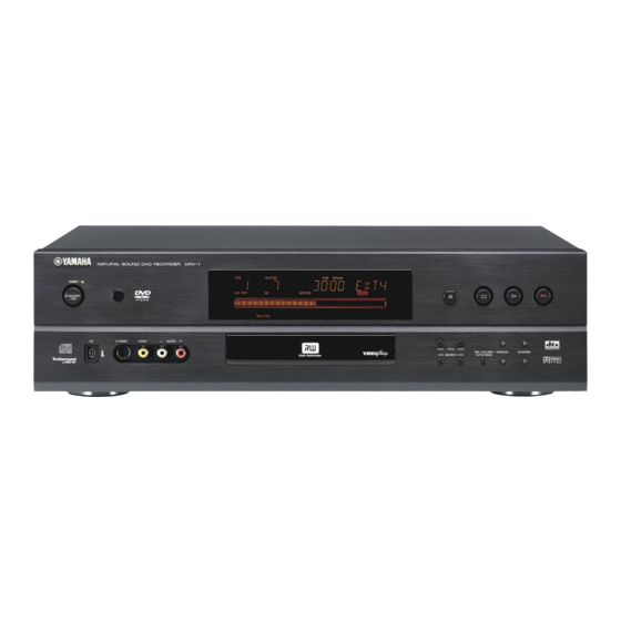
Page 5: Front Panels
DRX-1 FRONT PANELS U model NATURAL SOUND DVD VIDEO RECORDER DRX-1 STANDBY STANDBY S VIDEO VIDEO AUDIO TITLE REC VOLUME MANUAL CHANNEL SEARCH AUTO/MAN A model B model G model REMOTE CONTROL MONTER A/CH – – SELECT CLEAR MUTE TIMER... -
Page 6: Rear Panels
DRX-1 REAR PANELS U model A, B, G models SPECIFICATIONS VIDEO FORMAT DISC FORMATS SUPPORTED Digital Compression MPEG2 for DVD Disc type Playback Recording MPEG1 for VCD DVD+RW • • DVD+R • • VIDEO RESOLUTION 50Hz 60Hz DVD-RW (Video format) •... -
Page 7: Specifications
DRX-1 AUDIO FORMAT CABINET Compressed digital Playback Recording Dimensions (WxHxD) 435 x 120 x 330 (17 x 4.8 x 13 inches) • Dolby Digital (AC-3) Multi-channel 2-channel Net Weight 13.9 lb. (6.3 kg) 16 bit, fs 48 kHz Front Panel 3mm Aluminum •... - Page 8 DRX-1 V I D E O P l u s + a n d P l u s C o d e a r e r e g i s t e r e d VCR Plus+ and PlusCode are registered trademarks trademarks of Gemstar Development Corporation.The VCR Plus+...
-
Page 9: Disassembly Procedures
DRX-1 DISASSEMBLY PROCEDURES... -
Page 10: Service Position
DRX-1 DVIO 2 SERVICE POSITION Front Front Photo 4 Digital board Photo 1 After demounting of DVIO board, the top side of the digital board is in reach. To reach the bottom side of the digital board, the DVDR module must be demounted together with the digital board. - Page 11 DRX-1 Analog board To put the analog board in service position, demount the assembly of analog board and backplate as follows: 1. Remove 3 screws from the backplate to the frame 2. Remove the screw from the backplate to the mains inlet of the power supply 3.
-
Page 12: Diagnostic Software
DRX-1 DIAGNOSTIC SOFTWARE Due to the complexity of the DVD recorder, the time to find 1.2 Contents a defect in the recorder can become long. To reduce this Unplug the power cord time, the recorder has been equipped with Diagnostic and Hold key... - Page 13 DRX-1 AnalogueTuner checks whether the tuner on the analogue board is accessible LoopAudioUserDealer This nucleus tests the components on the audio signal path The host decoder - The analogue board - The audio encoder - The VSM On the analogue board the audio is internally looped back to the digital board...
- Page 14 DRX-1 STEP DESCRIPTION NUCLEUS The local display shows FPLED. Press PLAY to start the test. Press PLAY to confirm that the led is lit. Press RECORD to indicate that the led is not lit. Press STOP to skip this nucleus.
- Page 15 DRX-1 STEP DESCRIPTION NUCLEUS The local display shows BEWRITE READ. Press PLAY to start the test. Press STOP to skip this nucleus. The local display shows BETRAY OPEN. Press PLAY to start the test. Press STOP to skip this nucleus.
- Page 16 DRX-1 Player script Fig. 2...
-
Page 17
DRX-1 DIGITAL BOARD & FRONTPANEL ANALOG BOARD BASIC ENGINE TEST TEST TEST press
to execute press < STOP > to skip press to execute press to skip press to execute press < STOP > to skip press ... -
Page 18: Dvd Recorder
DRX-1 2.4 Trade Mode 3.2 Error Handling Each nucleus returns an error code. This code contains six numerals, which means: IF TRADE MODE OFF IF TRADE MODE ON [ XX YY ZZ ] UNPLUG THE RECORDER UNPLUG THE RECORDER Error code... - Page 19 DRX-1 Command Overview VSM [03] We provide an overview of the nuclei and their numbers. [xxyy] Nuclei This overview is preliminary and subject to modifications. Number Register Access Host Decoder [01] SDRAM Access [xxyy] Nuclei SDRAM Write Read Number Interrupt lines...
- Page 20 DRX-1 Basic Engine [06] [xxyy] Nuclei [xxyy] Nuclei Number Number Download Version S2B Pass Bargraph Level Adjustment S2B Echo Clock correction Version Clock reference Reset Re-virginise Recorder Focus On Flash Checksum Focus Off Tuner frequency selection Disc Motor On Set virgin bit...
- Page 21 DRX-1 Menu Structure Miscellanious [14] The following menu structure is given after starting up the [xxyy] Nuclei DVD recorder in menu mode. The symbol -> indicates that Number the current menu choice will invoke the display of a 1400 Clock 11.289 MHz submenu.
- Page 22 DRX-1 Sine Generate Menu Front Panel Menu 1.Sine On 1.Echo 2.Sine Burst 1kHz 2.Version 3.Sine Burst 12kHz 3.Flap Control -> 4.Segment Test -> VSM Menu 5.Light Labels 1.Register Access 6.Led test 2.SDRAM Access 7.Keyboard test 3.VSM SDRAM Write/Read 8.Remote Control 4.Interrupt Lines...
- Page 23 DRX-1 Basic Engine Radial Menu Script Menu 1.Radial On 1.User/Dealer Script 2.Radial Off 2.Player Script 3.Radial Initialisation 4. Nuclei Error Codes 4.Radial ATLS Calibration In the following table the error codes will be described. Basic Engine Sledge Menu 1.Sledge test...
- Page 24 DRX-1 Error Nr Error String Error Nr Error String 11500 “” 13700 “” 11501 “Init of I2C failed” 13701 “Turning off MacroVision failed” 11502 “The selection of the clock source failed” 20000 “” 11504 “The demute of the audio failed”...
- Page 25 DRX-1 Error Nr Error String Error Nr Error String 20500 “” 20902 “I2C bus busy before start” 20501 “Error audio encoder SRAM WRR cannot 20903 “EMPRESS access time-out” initialise I2C” 20904 “No acknowledge from the EMPRESS” 20502 “Error audio encoder SRAM WRR cannot 20905 “No data send to the EMPRESS”...
- Page 26 DRX-1 Error Nr Error String Error Nr Error String 30304 “Interrupt B wasn’t raised.” 50103 “The frontpanel could not be accessed by the ana-logue board.” 30305 “Interrupts A and B were raised.” 50200 “” 30400 “” 50204 “Execution of the command on the analogue 30401 “VSM SDRAM Bank1 Memory databus test...
- Page 27 DRX-1 Error Nr Error String Error Nr Error String 50703 “The frontpanel did not show a starburst.” 51701 “Execution of the command on the analogue board failed.” 50704 “The user skipped the FP-starburst test.” 51702 “The frontpanel could not be accessed by the 50705 “The user returned an unknown confirmation:...
- Page 28 DRX-1 Error Nr Error String Error Nr Error String 60106 “Wrong echo pattern received” 61502 “Parity error from Basic Engine to Serial” 60200 “Version: nr1.nr2.nr3” 61503 “Communication time-out error” 60201 “ B a s i c E n g i n e r e t u r n e d e r r o r n u m b e r 61504 “Unexpected response from Basic Engine”...
- Page 29 DRX-1 Error Nr Error String Error Nr Error String 61905 “Unexpected response from Basic Engine” 62900 “” 62000 “” 62901 “ B a s i c E n g i n e r e t u r n e d e r r o r n u m b e r 0xerrornumber”...
- Page 30 DRX-1 Error Nr Error String Error Nr Error String 63901 “ B a s i c E n g i n e r e t u r n e d e r r o r n u m b e r 64201 “BE i2c initialisation failed”...
- Page 31 DRX-1 Error Nr Error String Error Nr Error String 71301 “Routing the audio on the Analogue Board 73002 “Communication with Analogue Board fails” fails.” 73100 “0xslashversion”” where slashversion is the 71302 “Invalid input.” slash version read from the analogue board”...
- Page 32 DRX-1 Error Nr Error String Error Nr Error String 80300 “The accessibility of the DVIO module is OK.” 80412 “ W e t r i e d t o r e c e i v e a r e p l y f o r DVIO_MAX_RETRIES_REPLY times !!”...
- Page 33 DRX-1 Error Nr Error String Error Nr Error String 80603 “The DVIO module could not be reset.” 80713 “We tried to receive an Acknowledge for DVIO_MAX_RETRIES_ACK times!” 80604 “Unable to receive the reset indication from the DVIO module.” 80714 “VSM UART error timeout transmitting command”...
- Page 34 DRX-1 Error Nr Error String Error Nr Error String 90221 “The video encoder did not receive data from 90420 “The video encoder did not return the Group the VIP.” Of Picture count.” 90223 “Initialisation of VIP and EMPRESS failed” 90421 “The video encoder did not receive data from...
- Page 35 DRX-1 Error Nr Error String Error Nr Error String 90617 “VSM and Hostdec memory do not match 90812 “Error cannot initialise host decoder audio in” (com-pared after transfer)” 90813 “Error loop audio user/dealer cannot start 90618 “ D e c o d i n g o f t h e v i d e o d a t a i n t h e audio en-coder”...
- Page 36 DRX-1 Error Nr Error String Error Nr Error String 90920 “Error: audio data in host memory and VSM 141301 “Progressive Scan Route Enable failed” mem-ory differ” 141302 “Generating test image in Hostdecoder failed” 90921 “Error: audio data in host memory contains 141400 “”...
- Page 37 DRX-1 5.2 Nucleus 901: Audio User Dealer Loop 5.3 Nucleus 902: Digital Video Loop A PCM audio sine of 12kHz is generated in the Host A colourbar generated in the host decoder is looped Decoder for a while and sent to the analogue board. The...
- Page 38 DRX-1 5.4 Nucleus 903: Digital Video VBI Loop 5.5 Nucleus 904: System Video Loop Nucleus for testing the components on the video VBI Nucleus for testing the components on the video signal signal path: system path: • The VIP • The VIP •...
- Page 39 DRX-1 5.6 Nucleus 905: System Video VBI Loop 5.7 Nucleus 906: Video User Dealer Loop This nucleus tests the components on the video signal Nucleus for testing the components on the video signal path: system path: • The VIP • The VIP •...
- Page 40 DRX-1 5.8 Nucleus 907: Video VBI User Dealer Loop 5.9 Nucleus 908: System Audio Loop Scart (Europe) This nucleus tests the components on the video VBI signal Nucleus for testing the components on the audio signal path: path: • The VIP •...
- Page 41 DRX-1 5.10 Nucleus 909: System Audio Loop CINCH (Nafta) Nucleus for testing the components on the audio signal path: • The hostdecoder • The analogue board • The audio encoder • The VSM On the analogue board the audio is passed to the CINCH connector, where a CINCH cable needs to be used to loop back the audio signal to the digital board.
-
Page 42: Faultfinding Trees
DRX-1 FAULTFINDING TREES 1. General-1 PLAYBACK MODE Plug Recorder to the mains. No disc loaded Standby LED changes Check PSU(see chapter 2) from green to red. Check Analog PCB(see chapter 4) Display shows time Check Display PCB(see chapter 5) Press "STOP" button... -
Page 43: Record Mode
DRX-1 1. General-2 RECORD MODE Insert DVDR Disc Display shows: - Disc content - Check Basic Engine(see chapter 3) - Source - DVD+RW - Disc Bar Press NEXT button to select empty title Press "RECORD" button - Check Analog PCB(see chapter 4) -
Page 44: Power Supply
DRX-1 2. Power Supply Remove all the connectors from the PSU Check DC voltages on connector 0205: +12Vstby, +5V2stby, -5Nstby, -Vgnstby, +33Vstby None of the voltages are present +12Vstby and +5V2stby are OK. All voltages are present. Check +12Vreg circuit: Check +33Vstby circuit: Standby voltages are oke. - Page 45 DRX-1 3. Digital Board-1 START UP DSW NOT OK Check Power Supplies on con. 1900 - Check connection to PSU - Check Power Supply (ION should be LOW) Check that Sysclk_5505 on I819 - Check IC 7202 - Check IC 7916-C...
- Page 46 DRX-1 3. Digital Board-2 POWER PART CHECK DIGITAL BOARD USE DIGITAL BOARD CIRCUIT DIAGRAMS 1 2, 3, 4, 5, 7 AND 8 AND DIGITAL BOARD BOTTOM VIEW TESTPOINTS Power On and exit stand-by mode Check +3V3 on Testpoints I905 Check +12V on Testpoint I907...
- Page 47 DRX-1 3. Digital Board-3 RESET & CLOCK CHECK DIGITAL BOARD USE DIGITAL BOARD CIRCUIT DIAGRAMS 1,2,7 AND 8 AND DIGITAL BOARD BOTTOM VIEW TESTPOINTS Power on and exit stand-by mode - Check IC7902 Resetn(+3V3) on testpoint I912 - Check D6900...
- Page 48 DRX-1 3. Digital Board-4 DSW MEMORY TESTS Start Diagnostic Software and select Command mode Flash Checksum - Check IC 7301 Command: 100 - Check IC 7302 Flash 1 Write Access - Check IC 7301 Command: 101 Flash 2 Write Access...
- Page 49 DRX-1 3. Digital Board-5 DSW VSM TESTS Start Diagnostic Software and select Command mode VSM Interconnection Test - Check IC 7100 Command: 304 SDRAM Access Test - Check IC 7101 Command: 301 SDRAM Write/Read Test - Check IC 7100 Command: 302...
- Page 50 DRX-1 3. Digital Board-6 DSW AUDIO PART CHECK Start Diagnostic Software and select Command mode Audio Clock Test - Check IC 7900 Command: 1400 - Check IC 7906 Measure ACC_ACLK_PLL on I902 - Check IC 7100 (11.289MHz) Audio Clock Test...
- Page 51 DRX-1 3. Digital Board-7 DSW VIDEO PART CHECK Start Diagnostic Software and select Command mode - Check Analog Board Gateway Test to Analog Board Command: 700 - Check IC 7100 Color Bar ON Test Command: 120 Check Red Video Out on pin 5 of con.1601 Check Green Video Out on pin 3 of con.1601...
- Page 52 DRX-1 3. Digital Board-8 VIDEO PART CHECK PROGRESSIVE SCAN Start Diagnostic Software and select Command mode Generate NTSC Testpicture Command: 135 10 1 Switch off Macrovision Command: 137 Route PS to Analog Board Command: 1415 Route Video on Analog Board...
- Page 53 DRX-1 3. Digital Board-9 DSW BASIC ENGINE TESTS Start Diagnostic Software and select Command mode Basic Engine S2B Echo Test - Check IC 7202 Command: 601 - Check Basic Engine Basic Engine Tray Open Test - Check Basic Engine Command: 616...
- Page 54 DRX-1 3. Digital Board-10 Waveforms Digital Board Sysclk_VSM Sysclk_5505 2V / div DC 20ns / div 2V / div DC 20ns / div 27M_clk_PS acc_aclk_pll 2V / div DC 20ns / div 2V / div DC 50ns / div EMI_PROCCLK...
- Page 55 DRX-1 3. Digital Board-11 Waveforms Digital Board AD_WCLK; AE_WCLK AD_BCLK; AE_BCLK AD_ACLK 2V / div AC 10us / div 2V / div AC 200ns / div 2V / div AC 50ns / div AD_DATAO; AE_DATAO; AE_DATAI AD_DATAO; AE_DATAO; AE_DATAI AD_SPDIF...
- Page 56 DRX-1 3. Digital Board-12 Waveforms Digital Board DAC-B DAC-A/Y Cr-signal 500mV / div AC 10us / div 500mV / div AC 10us / div 500mV / div AC 10us / div DAC-C HS_IN VSOUT 500mV / div AC 10us / div...
- Page 57 DRX-1 4. Analog Board-1 Fig. 16...
- Page 58 DRX-1 4. Analog Board-2 Fig. 17...
- Page 59 DRX-1 4. Analog Board-3 Fig. 18...
- Page 60 DRX-1 4. Analog Board-4 Power Part Check Check internal Power supply voltages 5M on testpoint F9340 check Fuse 1327 12STBY on testpoint F810 check Fuse 1326 check IC 7332 8STBY on pin 3 of IC7332 8SW on testpoint F9336 check - ISTBY HIGH?
- Page 61 DRX-1 4. Analog Board-5 DSW CHECK ANALOGUE BOARD Start Diagnostic Software and select Command mode - Check Reset signal(+5V) on F902 - Check Clock(20MHz) on I915 Echo Test Analogue Board Command: 700 - Check connection to Digital Board - Check IC 7803...
- Page 62 DRX-1 4. Analog Board-6 Routing Audio and Video The paths that are available for video routing and their Route Video description (Nafta region) routed to the digital board. Nucleus Number: 712 Description PATH ID DESCRIPTION This nucleus routes the video signals on the analogue...
- Page 63 DRX-1 4. Analog Board-7 Route Audio PATH ID DESCRIPTION Nucleus Number: 713 Input signal is VIDEO(CVBS) from digital Description board and will be re-routed back to the digital This nucleus routes the audio on the analogue board to board. the destination determined by the input parameters.
- Page 64 DRX-1 5. Display Board TROUBLESHOOTING DISPLAY BOARD Check supply voltage NO DISC Connector1916-2 12STBY +12V POWER ON Connector1916-3 VGNSTB -32V Connector1916-11 5STBY Connector1916-12 +5.2V Check filament voltage Testpoint F105 12STBYSI +12V AC voltage is created via oscillator circuit (7152-7153). DISPLAY? Check heater voltage on testpoints F102 and F101 3.2VAC, -24,4VDC, 42 kHz.
- Page 65 DRX-1 6. DVIO Board-1 POWER PART CHECK DVIO USE DVIO BOARD CIRCUIT DIAGRAMS 1 2, 3, 4 AND 5 AND DVIOTOPVIEWTESTPOINTS Power On and exit stand-by mode +5V on testpoint F536 Check connector 1500 to Digital board +3V3 on testpoint F531...
- Page 66 DRX-1 6. DVIO Board-2 RESET & CLOCK CHECK DVIO USE DVIO BOARD CIRCUIT DIAGRAMS 2, 3, 4 AND 5 AND DVIO TOP VIEW TEST POINTS Power On and exit stand-by mode Enable DVIO board: - press channel up or down...
- Page 67 DRX-1 6. DVIO Board-3 DSW DVIO TESTS Start Diagnostic Software and select Command mode DVIO Board Presence Test - Check DVIO Board Command: 800 - Check Connector 1500 - Check IC7303 Reset DVIO Test - Check IC 7203 Command: 801...
- Page 68 DRX-1 6. DVIO Board-4 Waveforms DVIO uP_clock Clockaudtmp 2V / div DC 100ns / div 2V / div DC 50ns / div Clock 27MHz Clock 27M_DV 2V / div DC 20ns / div 2V / div DC 20ns / div...
-
Page 69: Alignments
DRX-1 1.2 HF - AGC adjustment [3707]: ALIGNMENTS Service tasks after replacement of IC 7703: 1. Alignment Instructions Analogue Board Purpose: Set amplifier control. Alignments Analog PCB Eur Symptom, if incorrectly set: Picture jitter if input level is too low and picture distortion ADJUSTMENT INSTRUCTIONS ANALOGUE BOARD if input level is too high. - Page 70 DRX-1 2.1 Bargraph 0db Alignment Reset of Slash Version For an exact functionality of the bar graph in the display, a Use command 729 to reset the analogue board to the correction factor for the left and the right channel is stored default setting.
- Page 71 DRX-1 3.4 Procedure B 1. Note the serial number of the set example: AH050136130156 – AH = production centre Hasselt. According to UAW- 500: A=1 and H=8 – 05 = change code (this is not used for this calculation) – 01 = YEAR –...
-
Page 72: Circuit Descriptions
DRX-1 CIRCUIT DESCRIPTION 1. Multi-Mode SOPS 50PS203 1.1. Why Multi-Mode SOPS? Using ordinary SOPS results in a decrease of the efficiency at low output loads due to the increase of the switching frequency. The Multi-Mode SOPS will reduce the switching frequency at low loads but still preserves valley switching. - Page 73 DRX-1 Control Circuit Overvoltage Protection Circuit The control circuit exists of T7140, D6141, C2144 and This circuit consists of R3149, D6144, 6143, R3144, 2145, C2147, R3147 and 3148. C2142 and T7142. This circuit is fed by supply voltage +Vb via R 3141. This...
- Page 74 DRX-1 2. Display Board Flap Motor: 2.1 Operation Unit DC (DC Part) The core element of the operation unit DC is the m i c r o c o n t r o l l e r T M P 8 8 C U 7 7 Z F [ 7 1 5 6 ] . T h e...
- Page 75 DRX-1 3. Analog Board Europe (A, B, G models) 3.7 Power Supply 3.1 Microprocessor TMP93C071F The 5SW and 8SW supply are switched off in case of The microcontroller „AIO“ TMP93C071F is a 16bit standby from the P via the ISTBY-line. This is possible for microcontroller with internal ROM and 8kB RAM.
- Page 76 DRX-1 determine the antenna signal strength after a buffer [7705] chinch (E6), Rear Chinch (E4), Scart 1 (E1) and Scart 2 (E2). with the signal AGC_MUTE. In the opposite direction this Rear Chinch In is routed via the pre selector BA 7652; the line may be used to mute the demodulator to avoid cross other signals are connected direct to the STV 6410.
- Page 77 DRX-1 • Bit 3 &2: not used Cinch input is routed via MSP3415 to the STV 6410. After • Bit 1 & 0: Status Scart-1/Pin8: selecting the audio source via STV 6410, the signal must – 0 1 Low-level be transformed into the digital domain. For this, the UDA –...
- Page 78 DRX-1 Fig. 4...
- Page 79 DRX-1 Fig. 5...
- Page 80 DRX-1 4. Analog Board Nafta version 4.7 Front End (TU, AP Part) 4.1 Microprocessor TMP93C071F The front end comprises the following parts: The microcontroller „AIO“ TMP93C071F is a 16bit • Tuner [1705] microcontroller with internal ROM and 8kB RAM. It •...
- Page 81 DRX-1 have bottom clamp, the chroma inputs have average • Y/C-Rear is determined via Port40/AIN3 (Pin14) of CC clamp, and the RGB switch has bottom clamp circuits at (WSRI-line) and Port41/AIN4 (Pin15) is used for Y/C- the inputs. The R/C inputs can be switched to average Front (WSFI-line).
- Page 82 DRX-1 Detailed Description UDA 1328: The UDA1328 is a 6 channel DAC employing bitstream conversion techniques, which can be used either in L3 microcontroller mode or in static pin mode. The UDA 1328 supports the I S-bus data format with word lengths of up to 24 bits.
- Page 83 DRX-1 Fig. 6...
- Page 84 DRX-1 Fig. 7...
- Page 85 DRX-1 5. Digital Board 5.3 S2B Interface 5.1 Record Mode The S2B interface between the VSM (IC7100) and the Video Part Servo processor MACE3 controls the Basic Engine during Analog Video input signals CVBS, YC and UV(RGB for record and playback mode.
- Page 86 DRX-1 Fig. 8...
- Page 87 DRX-1 6. Divio Board 5.10 Progressive Scan Description 6.1 Short Description of the Module: The progressive scan part is integrated in the Digital The DVIO Module is a decoder for DV streams. Input is a Board and built around the SAGE Fli2200 de-interlacer / stream from a DV-camcorder IEEE1394.
- Page 88 DRX-1 6.2 Block Diagram Fig. 11...
- Page 89 DRX-1 6.3 Functional Description Reset The DVIO module consists of the following blocks (see The FPGA controls the reset signals on the board. This blockdiagram): has the advantage that it is possible to reset the board 1. IEEE1394 Interface both from software and hardware.
- Page 90 DRX-1 Clock Circuit ClockGen regular clock Raw clock (CY2071) slow- (FPGA) loopfilter Fig. 13 The same can be applied for the audio clock. For this clock, a frequency of 8.192 MHz, 11.2896 MHz or 12.228 MHz is required. This depends on the sample-rate frequency(32kHZ, 44.1kHZ or 48kHZ)of the audio signal.
-
Page 91: Abbreviation List
DRX-1 ABBREVIATION LIST AE_BCLK_VSM Digital Board Audio Encoder I2S bit clock to VSM +12V AE_DATAI +12V Power Supply Audio Encoder Input data (PCM) +2V5_FLI AE_DATAI_DV +2V5 Power Supply for FLI Audio Encoder Input data (PCM) from DVIO +2V5_PLL AE_DATAO +2V5 Power Supply for PLL... - Page 92 DRX-1 BE_WCLK DV_IN_CLK Basic Engine I2S word clock Digital Video in clock from DVIO board C_IN DV_IN_DATA(7:0) Digital Video in data bus from DVIO board Video Chrominance input C_IN_VIP DV_IN_HS Chrominance input to Video Input Processor Digital Video in horizontal synchronisation from DVIO...
- Page 93 DRX-1 HD_M_DQ(15:0) RSTN_BE Host Decoder SDRAM data bus Reset control of basic engine HD_M_DQML RSTN_DVIO Reset control of DVIO Host Decoder SDRAM data mask enable(Lower) HD_M_DQMU RTS1P Host Decoder SDRAM data mask enable(Upper) Ready To Send data to service serial interface...
- Page 94 DRX-1 VCC3_CLK_BUF VIP_FB Power supply 3V3 clock buffer Video Input Processor Fast Blanking VCC3_VSM VIP_FID_FF Video Input Processor field indentifier to Flip Flop Power supply 3V3 Versatile Stream Manager VCC3_VSM_MEM VIP_HS Power supply 3V3 Versatile Stream Manager Memory Video Input Processor horizontal synchronisation...
- Page 95 DRX-1 VSM_UART2_RTSN AUD_BCLK Versatile Stream Manager UART2 received data to DVIO Audio Bit Clock board AUD_MUTE Audio Mute VSM_UART2_RX Versatile Stream Manager UART1 transmitted data to AUD_SDI analog Audio Serial Data Input AUD_SDO_CON board VSM_UART2_TX Audio Serial Data Output to buffer IC 7505...
- Page 96 DRX-1 DV_PDN PRSTN DVCODEC Power Down Processor reset DV_RSTN PWRN Processor write DVCODEC System Reset for NW701 DV_RWN RASN DVCODEC Read/Write control signal Row address strobe RESETN DV_VS DVCODEC Vertical synchronisation DVIO board reset FIFOA_A(0:15) RTSN FIFO buffer A Address bus...
-
Page 97: Ic Data
DRX-1 IC DATA UDA1328T: IC7001 V DDD V SSD UDA1328T STATIC MUTE DEEM1 CONTROL DEEM0 INTERFACE DIGITAL L3CLOCK DATAI12 INTERFACE DATAI34 L3DATA DATAI56 L3MODE VOLUME/MUTE/DE-EMPHASIS INTERPOLATION FILTER TEST1 TEST3 6-CHANNEL NOISE SHAPER SYSCLK TEST2 VOUT1P VOUT2P VOUT1N VOUT2N VOUT3 VOUT4... - Page 98 DRX-1 BA7660FS: IC7430 MUTE OUTA1 OUTA2 OUTB1 OUTB2 N.C. N.C. MUTE (1pin) OUTC1 3ch MUTE OUTC2 NORMAL STV6410: IC7507...
- Page 99 DRX-1 TMP93C071: IC7803...
- Page 100 DRX-1 STV5348: IC7990 UDA1334TS: IC7506...
- Page 101 DRX-1 SAA6752HS: IC7403...
- Page 102 DRX-1 SAA7118: IC7500 Bottom View MXXxxx SAA7118 SAA7108E SAA7109E 2 3 4 5 6 7 8 9 10 11 12 13 14 O utput F orm atter I-P ort IN T_A TM S S C L TC K S D A...
- Page 103 DRX-1 58PDI1394P25: IC7101 LREQ AGND SYSCLK CTL0 CTL1 PDI1394P25 AGND TPBIAS0 TPA0+ TPA0± TPB0+ TPB0± 33 AGND RECEIVED DATA CABLE POWER DECODER/ /ISO DETECTOR RETIMER C/LKON SYSCLK LREQ CABLE PORT 0 CTL0 LINK CTL1 INTERFACE TPA0+ TPA0± ARBITRATION TPB0+ AND CONTROL TPB0±...
- Page 104 DRX-1 P89C51RD: IC7203 Function Function Function NIC* P3.4/T0 P2.7/A15 P1.0/T2 P3.5/T1 PSEN ALE/PROG P1.1/T2EX P3.6/WR NIC* P1.2/ECI P3.7/RD EA/V P1.3/CEX0 XTAL2 P0.7/AD7 P1.4/CEX1 XTAL1 P0.6/AD6 P1.5/CEX2 P0.5/AD5 P1.6/CEX3 NIC* P0.4/AD4 P1.7/CEX4 P2.0/A8 P0.3/AD3 P2.1/A9 P0.2/AD2 P3.0/RxD P2.2/A10 P0.1/AD1 NIC* P2.3/A11 P0.0/AD0...
- Page 105 DRX-1 FLI2200 Ext. Syncs Ext. Syncs Sync Sync Sync Sync PLL/Clock PLL/Clock Generator Generator PIXCLK PIXCLK Generator Generator Deinterlacer Core with DCDi™, Deinterlacer Core with DCDi™, YU V/ YU V/ RGB /YUV/ RGB /YUV/ Input Input Output Output Motion Compensation,Film...
- Page 106 DRX-1 MEMO...
-
Page 107: Block Diagram
DRX-1 BLOCK DIAGRAM U model ANALOG INTELLIGENT CONTROL AUDIO L FRONT 1911 RC6 IN Analog input 1953 AFCRI AUDIO R AFCRI AFCLI ANALOG AUDIO VIDEO CVBSFIN AFCLI AUDIO DIGITAL CVBS CVBSFIN INPUT/OUTPUT CFIN AUDIO OPTICAL 1500 S-VIDEO DVIO CONTROL +3V3... - Page 108 DRX-1 BLOCK DIAGRAM A, B, G model ANALOG INTELLIGENT CONTROL FRONT AUDIO L 1911 Analog input 1953 AFCRI AUDIO R AFCRI AFCLI ANALOG AUDIO VIDEO CVBSFIN AFCLI AUDIO DIGITAL CVBS CVBSFIN INPUT/OUTPUT CFIN 1500 AUDIO OPTICAL S-VIDEO DVIO +3V3 CFIN...
-
Page 109: Wiring Diagram
DRX-1 WIRING DIAGRAM 8001 8002 1602 1900 1601 1954 GNDD B_OUT_B SPDIF GNDD COAX_IN G_OUT_B OPT_IN GNDD R_OUT_B +3V3 GNDD MUTEN C_OUT_B GNDD GNDD AD_ACLK Y_OUT_B GNDD GNDD 1962 8015 AD_DATAO CVBS_OUT_B 1800 1962 AD_WCLK GNDD GNDD GNDD AD_BCLK CVBS_Y_IN... -
Page 110: Printed Circuit Board
DRX-1 PRINTED CIRCUIT BOARD A, B, G model POWER SUPPLY P. C. B. (Top View) 0101 A1 0209 B6 1520 B5 2130 A3 2212 A5 2240 A5 2521 B6 3128 A3 3141 B3 3223 A6 5115 A1 5501 A7 6129 B1... - Page 111 DRX-1 PRINTED CIRCUIT BOARD A, B, G model POWER SUPPLY P. C. B. (Bottom View) 2139 A2 2143 A2 2151 A2 2222 A5 2511 B6 3140 A4 3145 A2 3220 B6 3234 B7 3502 B7 3512 B6 3520 B5 3524 B6...
- Page 112 DRX-1 PRINTED CIRCUIT BOARD A, B, G model POWER SUPPLY P. C. B. (Part 1 Top View)
- Page 113 DRX-1 PRINTED CIRCUIT BOARD A, B, G model POWER SUPPLY P. C. B. (Part 2 Top View)
- Page 114 DRX-1 PRINTED CIRCUIT BOARD DISPLAY P. C. B. (Top View) IR & STANDBY P. C. B. (Top View) DISPLAY P. C. B. (Bottom View) IR & STANDBY P. C. B. (Bottom View)
- Page 115 DRX-1 PRINTED CIRCUIT BOARD FRONT AV INPUT P. C. B. FRONT DV INPUT P. C. B. 2100 3113 2101 4101 2102 4102 2103 6100 0002 C1 2104 6101 2105 6102 0003 A2 2106 6103 1000 C1 3100 6104 3101 7100...
- Page 116 DRX-1 PRINTED CIRCUIT BOARD U model ANALOG P. C. B. (Overview Top View) 1324 1953 2000 2030 2475 2523 2558 2810 3006 3403 3500 3819 3862 3888 3924 3981 4971 6805 7507 7901 1325 1954 2003 2201 2476 2525 2559...
- Page 117 DRX-1 PRINTED CIRCUIT BOARD U model ANALOG P. C. B. (Part 1 Top View)
- Page 118 DRX-1 PRINTED CIRCUIT BOARD U model ANALOG P. C. B. (Part 2 Top View)
- Page 119 DRX-1 PRINTED CIRCUIT BOARD U model ANALOG P. C. B. (Overview Bottom View) 2001 2321 2472 2607 2715 2907 3016 3109 3329 3416 3481 3564 3709 3729 3836 3907 5700 6439 6902 7706 2002 2322 2473 2609 2802 2908 3017...
- Page 120 DRX-1 PRINTED CIRCUIT BOARD U model ANALOG P. C. B. (Part 1 Bottom View)
- Page 121 DRX-1 PRINTED CIRCUIT BOARD U model ANALOG P. C. B. (Part 2 Bottom View)
- Page 122 DRX-1 PRINTED CIRCUIT BOARD U model ANALOG P. C. B. (Testlands Top View)
- Page 123 DRX-1 PRINTED CIRCUIT BOARD U model ANALOG P. C. B. (Testlands Bottom View) RSVHSCIn AROut_1 ALOut_1 ALOut_2 AROut_2 RCVBSIn V_IN GNDV DIG OUT H RSVHSYIn FAN_IN RCVBSOut1 Y_IN RC IN RSVHSCOut RSVHSYOut ALIn_1 OPT OUT Y_OUT ARIn_1 RCVBSOut2 U_IN DIG OUT L...
- Page 124 DRX-1 PRINTED CIRCUIT BOARD A, B, G model ANALOG P. C. B. (Overview Top View)
- Page 125 DRX-1 PRINTED CIRCUIT BOARD A, B, G model ANALOG P. C. B. (Part 1 Top View)
- Page 126 DRX-1 PRINTED CIRCUIT BOARD A, B, G model ANALOG P. C. B. (Part 2 Top View)
- Page 127 DRX-1 PRINTED CIRCUIT BOARD A, B, G model ANALOG P. C. B. (Overview Bottom View)
- Page 128 DRX-1 PRINTED CIRCUIT BOARD A, B, G model ANALOG P. C. B. (Part 1 Bottom View)
- Page 129 DRX-1 PRINTED CIRCUIT BOARD A, B, G model ANALOG P. C. B. (Part 2 Bottom View)
- Page 130 DRX-1 PRINTED CIRCUIT BOARD A, B, G model ANALOG P. C. B. (Testlands Top View)
- Page 131 DRX-1 PRINTED CIRCUIT BOARD A, B, G model ANALOG P. C. B. (Testlands Bottom View) 8_SC1 Gout_SC1 RSVHSCIn RCALOut RCAROut RCVBSIn RCVBSOut YCVBSOut_SC1 P50_SC1 DIG OUT H RSVHSYIn ALIn_SC1 RCOut_SC1 BC_SC1 AROut_SC1 ARCLI RSVHSCOut ARIn_SC1 OPT OUT DIG OUT L...
- Page 132 DRX-1 PRINTED CIRCUIT BOARD DVIO P. C. B. (Overview Top View)
- Page 133 DRX-1 PRINTED CIRCUIT BOARD DVIO P. C. B. (Part 1 Top View)
- Page 134 DRX-1 PRINTED CIRCUIT BOARD DVIO P. C. B. (Part 2 Top View)
- Page 135 DRX-1 PRINTED CIRCUIT BOARD DVIO P. C. B. (Testlands Bottom View)
- Page 136 DRX-1 PRINTED CIRCUIT BOARD DIGITAL P. C. B. (Overview Top View) 1100 2311 2707 3221 3909 PART 1 1101 2403 2708 3222 4102 1200 2411 2709 3223 4103 1500 2412 2710 3224 4104 1600 2413 2711 3225 4105 1601 2417...
- Page 137 DRX-1 PRINTED CIRCUIT BOARD DIGITAL P. C. B. (Part 1 Top View) PART 1...
- Page 138 DRX-1 PRINTED CIRCUIT BOARD DIGITAL P. C. B. (Part 2 Top View) PART 2...
- Page 139 DRX-1 PRINTED CIRCUIT BOARD DIGITAL P. C. B. (Overview Bottom View) 2104 2802 3803 7702 2105 2803 3804 7800 2106 2804 3805 7801 PART 1 2107 2805 3806 7900 2108 2806 3809 7901 2115 2807 3810 7902 2120 2808 3811...
- Page 140 DRX-1 PRINTED CIRCUIT BOARD DIGITAL P. C. B. (Part 1 Bottom View) PART 1...
- Page 141 DRX-1 PRINTED CIRCUIT BOARD DIGITAL P. C. B. (Part 2 Bottom View) PART 2...
- Page 142 DRX-1 PRINTED CIRCUIT BOARD DIGITAL P. C. B. (Testlands Bottom View) Resetn_BE +3V3 +3V3 +12V +3V3 Resetn_VE +3V3 Resetn +3V3 +3V3 Sysclk_Empress EMI_PROCCLK Sysclk_ProgScan AE_DATAO ACC_ACLK_OSC Sysclk_VSM_5508 +3V3 VSYNC HSYNC VE_DSn VE_DTACKn +3V3 ACC_ACLK_PLL +3V3 +3V3 Mute VIP_ICLK +3V3 VSOUT...
-
Page 143: Printed Circuit Board
DRX-1 PRINTED CIRCUIT BOARD DIGITAL P. C. B. (Mapping Testlands) F214 A3 I175 A3 I300 A2 I610 A5 I720 B3 I880 C3 F247 A2 I176 A3 I301 A2 I611 B5 I721 B2 I881 C3 F248 A2 I177 A3 I302 A2... - Page 144 DRX-1 SCHEMATIC DIAGRAM A, B, G model POWER SUPPLY 6130 D7 0101-1 B1 0101-2 A1 6131 D7 0125 C6 6132 D7 0205 F12 6140 C5 POWER SUPPLY 0210 C8 6141 D4 0240 D8 6142 D6 0260 D8 6143 E6 6144 E6...
-
Page 145: Schematic Diagram
DRX-1 SCHEMATIC DIAGRAM A, B, G model POWER SUPPLY 0200 G10 0201 G11 0202 G11 POWER SUPPLY 0207 B8 0209 A10 0221 B3 1520 B4 2501 D4 2502 D5 2506 F4 2511 E9 2512 E10 0209 EH-B 2513 E11 +3V3... - Page 146 DRX-1 SCHEMATIC DIAGRAM DISPLAY 0201 I1 6177 D4 0202 I2 6178 D4 0203 I3 6179 D4 0206 0204 I4 6180 D4 12STBY 12STBYSI DISPLAY HOLDER 0206 A12 6181 D3 STEREO NICAM DIGITAL MANUAL AC-3 MPEG PROLOGIC 1150 A1 6182 D3...
- Page 147 DRX-1 SCHEMATIC DIAGRAM FRONT AV INPUT 1910-A D1 1910-B B1 1910-C C1 1910-D F1 OPTION 1911 D8 2100 A6 2101 A5 2102 B3 2103 C6 2104 C5 2105 D3 2106 F2 I300 F200 3101 2101 3100 A5 I301 7100 3101 A3...
- Page 148 DRX-1 SCHEMATIC DIAGRAM IR AND STANDBY FRONT DV INPUT 0002 C3 1000 B1 1002 A1 2001 A1 2003 D2 5000 B2 6000 A2 0003 D3 1001 B2 2000 A2 2002 D2 3000 D2 5001 C2 6001 C2 1140 D2 1915 C1...
- Page 149 DRX-1 SCHEMATIC DIAGRAM U model ANALOG: All in One 1 1802 H5 7805 D3 I975 D4 1980 A10 7806 E2 I976 D7 All In One 1 12STBY AIO1 1981 D13 7807 F5 I977 C7 to EPG 1982 H14 7809 F4...
- Page 150 DRX-1 SCHEMATIC DIAGRAM U model ANALOG: All in One 2 1994 I3 2900 A2 All In One 2 AIO2 Pos. 3920, 3921,3922, 7902,7903, 7904 are for "ON-BOARD-PROGRAMMING" 2901 B14 5STBY2 2902 B13 2903 B14 5STBY2 2904 H14 5STBY2 2905 H14...
- Page 151 DRX-1 SCHEMATIC DIAGRAM U model ANALOG: TUBER / DEMODULATOR 1700 A5 2700 A2 2705 A9 2710 A8 2715 D7 3701 A3 3706 A8 3711 A1 3716 B1 3721 E10 3727 E8 4702 E5 5704 C2 6701 C4 7702 C4 7707 E3...
- Page 152 DRX-1 SCHEMATIC DIAGRAM U model ANALOG: IN / OUT 1 1951 A14 I/O 1 6512 H9 I576 C4 1953 I1 6900 D13 I580 D12 5STBY 5STBY 1954 I3 6901 E13 I581 E12 2500 2501 In / Out 1 1956-A I8...
- Page 153 DRX-1 SCHEMATIC DIAGRAM U model ANALOG: IN / OUT 2 1952-A C1 1955-B A1 1958-A F1 1959-A D1 In / Out 2 I/O 2 2400 B5 2401 B2 5STBY2 5STBY2 5STBY 2402 C9 2403 C9 2405 C9 2406 E4 REAR_IN...
- Page 154 DRX-1 SCHEMATIC DIAGRAM U model ANALOG: IN / OUT 3 1955-A B9 1955-C C9 1961-A F9 5STBY In / Out 3 1961-B E9 I/O 3 1962 F6 1992 E1 3439 F5205 REAR_OUT 1 1993 F1 1997-B B9 6432 CVBS 1997-C A9...
- Page 155 DRX-1 SCHEMATIC DIAGRAM U model ANALOG: SOUND PROCESSING 1600 F6 Sound Processing 1960 D1 GNDA 2600 A5 I602 2601 A6 2602 A6 GNDD GNDD 2603 A7 2604 A8 2605 B8 I604 3600 2606 B8 C670 I601 2607 C1 I603 2608 C9...
- Page 156 DRX-1 SCHEMATIC DIAGRAM U model ANALOG: POWER SUPPLY 1324 E8 1325 C8 1326 B2 1327 B2 Power Supply 1932 C1 1996 D4 2321 C6 12STBY 2322 D6 2323 D6 2324 B3 2325 B4 7332 2328 C8 2329 E2 I345 2330 B3...
- Page 157 DRX-1 SCHEMATIC DIAGRAM U model ANALOG: AUDIO CONVERTER Audio Converter DAC_ADC 1900 B1 F0002 E2 2000 A4 F0003 D2 2001 E1 F0005 D2 3000 2002 C7 F0007 D2 I028 3001 2003 C4 F0009 D2 GNDD GNDD GNDD GNDD 2004 C4...
- Page 158 DRX-1 SCHEMATIC DIAGRAM U model ANALOG: RGB-YUV CONVERTER ANALOG: DIGITAL IN / OUT 2200 A1 3200 A4 3210 C2 3214 E2 3220 E3 7200-B D3 I201 A2 I207 B1 I212 C2 I216 D4 1941-A A4 2472 A3 2479 C3 3472 A2...
- Page 159 DRX-1 SCHEMATIC DIAGRAM U model ANALOG: FAN CONTROL 1983 B5 2985 A3 3948 C3 3974 E1 3982 E3 3996 A4 7970-C E3 F806 C5 I924 E3 I932 A1 1984 C5 3940 C4 3967 A3 3975 E2 3983 E3 3997 A5...
- Page 160 DRX-1 SCHEMATIC DIAGRAM A, B, G model ANALOG: All in One 1 1802 H4 3916 F11 I887 I1 1980 A10 3917 F11 I888 I1 1981 D13 4801 D13 I890 D1 1982 H14 4906 G2 I891 D2 AIO1 All In One 1...
- Page 161 DRX-1 SCHEMATIC DIAGRAM A, B, G model ANALOG: All in One 2 1994 I3 2900 A2 All In One 2 AIO2 Pos. 3920, 3921,3922, 7902,7903, 7904 are for "ON-BOARD-PROGRAMMING" 2901 B14 5STBY2 2902 B13 2903 B14 5STBY2 2904 H14 5STBY2...
- Page 162 DRX-1 SCHEMATIC DIAGRAM A, B, G model ANALOG: TUNER / DEMODULATOR 1700 B5 2700 A3 2705 A9 2710 A8 2715 D7 3701 A6 3706 A8 3711 A1 3716 C1 3721 E10 3726 D9 4701 C4 5702 A5 5707 E10 7700 A10...
- Page 163 DRX-1 SCHEMATIC DIAGRAM A, B, G model ANALOG: IN /OUT 1 1950-1 E14 3560 B2 I541 E9 1950-3 H14 3561 B3 I542 E9 1951-C A14 3562 D13 I543 E11 In / Out 1 5STBY 5STBY I/O 1 1952-C C14 3563 C14...
- Page 164 DRX-1 SCHEMATIC DIAGRAM A, B, G model ANALOG: IN /OUT 2 1951-A F1 1952-A D1 1955-B A1 1958-A E1 1959-A C1 2410 2400 B5 2401 B2 2402 C9 REAR_IN 2403 C9 S-CONN 2404 C4 GNDV 2405 C9 1955-B 2406 E4...
- Page 165 DRX-1 SCHEMATIC DIAGRAM A, B, G model ANALOG: IN /OUT 3 1951-B F9 1952-B C9 REAR_OUT 5SWS 1955-A A9 1955-C B9 GNDV 1956 D9 1955-A 1958-B E9 TCX0310 1959-B C9 1991 F1 3432 F338 5SWS 7430 1992 E1 BA7660FS 2430 B6...
- Page 166 DRX-1 SCHEMATIC DIAGRAM A, B, G model ANALOG: IN /OUT 4 1950-2 C9 I464 A6 2460 A5 I465 C5 2461 B5 I469 A5 In / Out 4 I/O 4 2462 B5 I471 F8 2463 C5 I472 A7 2464 C2 I473 B7...
- Page 167 DRX-1 SCHEMATIC DIAGRAM A, B, G model ANALOG: SOUND PROCESSING 1600 F7 1960 D1 2600 A6 2601 A6 Sound Processing 2602 A7 2603 A7 GNDA 2604 A9 GNDD GNDD I602 2605 B8 2606 B8 2607 C2 2608 C9 2609 C2...
- Page 168 DRX-1 SCHEMATIC DIAGRAM A, B, G model ANALOG: FOLLOW ME ANALOG: VPS 2950 A1 2954 D2 3950 A1 3954 B1 3958 C3 3962 E2 3966 E4 7950 D4 I951 B2 I955 C1 I959 D3 I963 E1 1990 D1 2992 A3...
- Page 169 DRX-1 SCHEMATIC DIAGRAM A, B, G model ANALOG: POWER SUPPLY 1324 E8 Power Supply 1325 C8 1326 B2 1327 B2 1932 C1 12STBY 1996 D4 2321 C6 2322 D6 2323 D6 7332 2324 B3 2325 B4 I345 2328 C8 8STBY...
- Page 170 DRX-1 SCHEMATIC DIAGRAM A, B, G model ANALOG: AUDIO CONVERTER 1900 B1 5002 B3 2000 A4 5003 B1 2001 E1 5004 B1 I001 6000 3044 3000 2002 C7 6000 A1 IPFAIL 7011 5STBY 5NSTBY GNDA from AIO1 I028 digital silence muting...
- Page 171 DRX-1 SCHEMATIC DIAGRAM A, B, G model ANALOG: RGB-YUV-CONVERTER ANALOG: DIGITAL IN / OUT 2200 A1 3202 B2 3208 C1 3214 D2 3222 E2 4203 D4 I201 A2 I207 A1 I213 D1 I226 E2 1941-A A4 2471 A3 2481 E2...
- Page 172 DRX-1 SCHEMATIC DIAGRAM A, B, G model ANALOG: FAN CONTROL 1983 C5 2985 B3 3948 D2 3974 F1 3982 E3 3996 A4 7970-C E3 F806 C5 I924 F3 I932 B1 1984 C5 3940 C4 3967 A3 3975 F2 3983 F3...
- Page 173 DRX-1 SCHEMATIC DIAGRAM DVIO: 1394 INTERFACE 1400 F3 1901 B1 2400 F8 2401 C2 3V3_D 3V3_A 2402 C2 1394 INTERFACE 2403 E1 2404 E1 2405 E2 2406 E2 3V3_A 2407 E2 2408 E2 7400 2412 F4 UPD72852 2413 F3 DVDD...
- Page 174 DRX-1 SCHEMATIC DIAGRAM DVIO: MICROPROCESSOR 1902 B14 3558 H4 1905 A6 3559 I7 2431 D11 3560 I7 2432 D12 3561 I7 2433 D12 3562 F2 2434 D12 3563 H2 2435 D12 3564 E4 3V3_LINK 2436 E12 5431 C12 DV_STATUS 3472...
- Page 175 DRX-1 SCHEMATIC DIAGRAM DVIO: FIFO & CONTROL 1800 C6 F837 C2 1903 E13 F838 C2 1904 G12 F839 E2 2801 B6 2802 C6 2803 E13 uP- Part 2804 E13 2805 C2 3V3_uP 3V3_uP 3V3_uP 2806 C5 3V3_uP 3V3_uP 2807 H11...
- Page 176 DRX-1 SCHEMATIC DIAGRAM DVIO: DVCODEC 0003 I4 F542 G14 0004 I5 F543 G14 0005 I5 F544 G13 0006 I6 F545 G11 0007 I7 F547 G9 Interface + DAC 1500 C7 F548 G13 1501 H14 F549 H7 1502 E9 F550 G7...
- Page 177 DRX-1 SCHEMATIC DIAGRAM DVIO: AUDIO & VIDEO OUTPUT 2600 B4 2601 C5 2602 D3 2603 D5 2604 E3 2605 E2 3V3_LINK 2606 F8 3V3_AC 3V3_LINK 3V3_AC 3V3_AC 3V3_AC 3V3_AC 2616 2607 A8 5603 5601 2608 B7 100n 2609 A8 100MHZ...
- Page 178 DRX-1 SCHEMATIC DIAGRAM DIGITAL: VSM, BUFFER MEMORY AND BIT ENGINE INTERFACE 1100 2106 2114 2122 2130 2139 2147 3102 3110 3118 3126 3134 4103 7101 1101 2107 2115 2123 2131 2140 2148 3103 3111 3119 3127 3135 4104 7102 2100...
- Page 179 DRX-1 SCHEMATIC DIAGRAM DIGITAL: AV DECODER STI5508 1200 5207 2200 5208 2201 5209 F265 2202 5210 AV decoder : STI5508 GNDD 2203 5211 connector VDD_CORE 2204 5212 2205 7200 2206 7201 2207 7202-A C13 I2C BUS I264 2231 5209 2208...
- Page 180 DRX-1 SCHEMATIC DIAGRAM DIGITAL: AV DECODER MEMORY 2300 SDRAM Interface 2301 AV Decoder Memory 2302 SYSTEM DATA BUS 2303 I300 VDD_STI 2304 2305 SYSTEM ADDRESS BUS 2306 2307 7300 MT48LC4M16A2TG-7E 2308 14 27 43 49 GNDD 2309 GNDD VDDQ 2310...
- Page 181 DRX-1 SCHEMATIC DIAGRAM DIGITAL: VIDEO ENCODER, EMPRESS 2402 D_EMPRESS(15:0) 2403 Video Encoder Empress 2404 SMA(17:0) 2405 2406 SMD(15:0) 2407 {SM_WEN,SM_OEN,SM_CS0N,SM_CS3N,SM_UBN,SM_LBN} 2408 I410 5402 +3V3 2409 100MHZ 2410 2411 GNDD 2412 2413 2414 VDD_EMP_CORE VDD_EMP GNDD 2415 5400 I412 I413 2416...
- Page 182 DRX-1 SCHEMATIC DIAGRAM DIGITAL: VIP CVBS Y/C VIDEO INPUT 1500 2500 VIP CVBS Y/C Video Input 2501 2502 I508 5500 2503 +3V3 2504 100MHZ VDDA1A_7118 I509 5507 2505 +3V3 2506 100MHZ 2507 +3V3 2508 I510 5501 GNDD 2509 +3V3 100MHZ...
- Page 183 DRX-1 SCHEMATIC DIAGRAM DIGITAL: ANALOG P.C.B. CONS. VIDEO IN / OUTPUT 1600 7202-C D12 Analog P.C.B. Cons. AUDIO ENCODER VIP ANALOG VIDEO INPUT 1601 7600 DATA STREAM BUS 1602 7601 I664 AE_BCLK 1603 7602 Video In / Output I649 I660...
-
Page 184: Progressive Scan
DRX-1 SCHEMATIC DIAGRAM DIGITAL: PROGRESSIVE SCAN 2700 3719-A H9 2701 3719-B H8 Progressive Scan 2702 3719-C H8 2703 3719-D H8 2704 3720 I712 OPTION 2705 4700 +2V5_PLL 2706 4701 4700 7703 2707 4702 LF25C 2708 5700 I709 5701 I711 GNDD... - Page 185 DRX-1 SCHEMATIC DIAGRAM DIGITAL: PROGRESSIVE SCAN 1800 2806 2812 2818 2824 2832 3800 3806 3812 3818 3824 5801 5807 7802 2800 2807 2813 2819 2826 2833 3801 3807 3813 3819 3825 5802 5808 7803-A D14 2802 2808 2814 2820 2827...
- Page 186 DRX-1 SCHEMATIC DIAGRAM DIGITAL: POWER, CLOCK, AND RESET AUDIO CLOCK 1900 1900 Power, Clock and Reset - AudioClock 1901-1 G13 I931 5900 BLM31 I905 1901-2 F13 +3V3 100MHZ 1901-3 G13 5903 I900 2906 2900 1901-4 H13 VDD5_MK2703 100MHZ 1901-5 F13...
-
Page 187: Exploded View
DRX-1 EXPLODED VIEW U model When disassembling, use the special screw driver with tip shape in figure. 2.7 mm for screws 21, 34 and 35 2.2 mm for screws 32 1.7 mm for screws 22, 31 and 33 DVDR LOADER... - Page 188 DRX-1 EXPLODED VIEW A, B, G model When disassembling, use the special screw driver with tip shape in figure. 2.7 mm for screws 21, 34 and 35 2.2 mm for screws 32 1.7 mm for screws 22, 31 and 33...
-
Page 189: Mechanical Parts List
DRX-1 WARNING Components having special characteristics are marked s and must be replaced with parts having specifications equal to those originally in- MECHANICAL PARTS stalled. Ref. Ref. PART NO. Description Remarks Markets PART NO. Description Remarks Markets AAX44090 TRAY LID... -
Page 190: Exploded View (Front Ass'y)
DRX-1 EXPLODED VIEW (FRONT ASS’Y) for plastic parts for plastic parts... -
Page 191: Mechanical Parts List (Front Ass'y)
DRX-1 WARNING Components having special characteristics are marked s and must be replaced with parts having specifications equal to those originally MECHANICAL PARTS (Front Ass’y) MECHANICAL PARTS (Accessories) installed. Ref. Ref. PART NO. Description Remarks Markets PART NO. Description Remarks... - Page 192 DRX-1 DRX-1...