Sony MDR-NC500D Servise Manual
Noise canceling headphones
Hide thumbs
Also See for MDR-NC500D:
- User manual ,
- Product information (88 pages) ,
- Operating instructions manual (27 pages)
Table of Contents
Quick Links
SERVICE MANUAL
Ver. 1.2 2008.10
General
Type
Driver unit
Power handling capacity
Impedance
Sensitivity
Frequency response
Total Noise Suppression Ratio
*1
Power source
Mass
Supplied accessories
Connecting cord (0.5 m, gold plated stereo mini plug) (1)
Connecting cord (1.5 m, gold plated L type stereo mini plug) (1)
Connecting cord with battery case (1)
Carrying case (1)
Plug adaptor for in-fl ight use
*3
(single/dual) (1)
Gold-plated unimatch plug adaptor
(stereo phone plug y stereo mini jack) (1)
Sony LR6 (size AA) batteries (2) (US and Tourist models)
AC power adaptor (1)
Operating Instructions (1)
Product Information (1)
Startup guide (1)
Card warranty (1)
*1
Under the Sony measurement standard.
For details about the Total Noise Suppression
Ratio amount for each mode, refer to the
Product Information booklet.
Equivalent to approx. 99 % reduction of energy of sound compared
*2
with not wearing headphones
(NC MODE A).
May not be compatible with some in-fl ight music services.
*3
Design and specifi cations are subject to change without notice.
Sony Corporation
9-889-146-03
2008J05-1
Audio&Video Business Group
©
2008.10
Published by Sony Techno Create Corporation
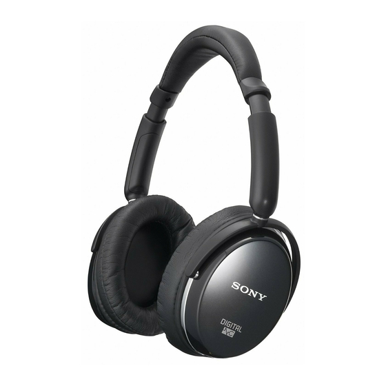
MDR-NC500D
SPECIFICATIONS
Closed dynamic
40 mm, dome type (CCAW adopted)
100 mW
40 Ω at 1 kHz
102 dB/mW
5 - 24,000 Hz
Approx. 20 dB
*2
DC 3.7 V: Built-in lithium-ion
rechargeable battery,
2 × LR6 (size AA) batteries,
or AC power adaptor
Approx. 195 g (6.9 oz)
General charging and usage time
Charging time
Usage time
Approx. 3 hours
*2
Approx. 15 hours
*1
At 1 kHz, 0.1 mW + 0.1 mW output
*2
Hours required to fully charge an empty battery
Time stated above may vary, depending on ambient temperature or
*3
conditions of use.
Battery life
Battery type
Approx. hours
Sony Alkaline
10 hours
LR6 (size AA) battery
*1
Output at 1 kHz, 0.1 mW + 0.1 mW
Time stated above may vary, depending on ambient temperature or
*2
conditions of use.
Note (US and Tourist models)
Because the supplied battery was included in the package from the time of
manufacture (as a convenience to the user), it is possible that the battery
life may be somewhat depleted by the time of purchase. The actual life
of the supplied battery may be shorter than the standard time described in
this manual when using a fresh battery.
NOISE CANCELING HEADPHONES
US Model
Canadian Model
AEP Model
UK Model
E Model
Australian Model
Chinese Model
Tourist Model
*1
*3
*1
*2
Table of Contents

Related Manuals for Sony MDR-NC500D


Summary of Contents for Sony MDR-NC500D
- Page 1 (stereo phone plug y stereo mini jack) (1) life may be somewhat depleted by the time of purchase. The actual life Sony LR6 (size AA) batteries (2) (US and Tourist models) of the supplied battery may be shorter than the standard time described in AC power adaptor (1) this manual when using a fresh battery.
-
Page 2: Table Of Contents
LES DIAGRAMMES SCHÉMATIQUES ET LA LISTE DES PIÈCES SONT CRITIQUES POUR LA SÉCURITÉ DE FONC- TIONNEMENT. NE REMPLACER CES COMPOSANTS QUE PAR DES PIÈCES SONY DONT LES NUMÉROS SONT DON- NÉS DANS CE MANUEL OU DANS LES SUPPLÉMENTS PUBLIÉS PAR SONY. -
Page 3: Servicing Notes
MDR-NC500D SECTION 1 SERVICING NOTES UNLEADED SOLDER Boards requiring use of unleaded solder are printed with the lead- free mark (LF) indicating the solder contains no lead. (Caution: Some printed circuit boards may not come printed with the lead free mark due to their particular size) : LEAD FREE MARK Unleaded solder has the following characteristics. -
Page 4: General
8 seconds and the If the MONITOR button is pressed and held while The POWER indicator on the battery case with Sony’s unique DNC Software POWER indicator blinks slowly. the POWER switch is set to ON, playback silences Press the AI NC MODE button. -
Page 5: Disassembly Flow
MDR-NC500D SECTION 3 DISASSEMBLY • This set can be disassembled in the order shown below. 3-1. DISASSEMBLY FLOW – Rch – – Lch – 3-2. MAIN BOARD (Rch) 3-3. BATTERY (LI-ION) (Page 6) SUB ASSY (Lch) (Page 7) 3-4. CHARGER BOARD (Lch) (Page 8) 3-5. -
Page 6: Main Board (Rch)
MDR-NC500D Note: Follow the disassembly procedure in the numerical order given. 3-2. MAIN BOARD (Rch) ear pad (R) housing (R) sub assy screen two screws (M2.6) claw Remove solders. MAIN board shield sheet (C) sheet (A) claw Remove solders. flexible flat cable... -
Page 7: Battery (Li-Ion) Sub Assy (Lch)
MDR-NC500D 3-3. BATTERY (LI-ION) SUB ASSY (Lch) screen shield sheet (B) ear pad (L) battery (LI-ION) sub assy lead CN403 black CHARGER board two screws (M2.6) sheet (B) battery (LI-ION) sub assy connector housing (L) sub assy 3-4. CHARGER BOARD (Lch) -
Page 8: Wire Setting
MDR-NC500D 3-5. WIRE SETTING – Lch – – Rch – sheet (A) relay cord relay cord driver wire driver wire MIC NC wire MIC NC wire relay cord wire MIC monitor wire ground wire JACK wire JACK board flexible flat cable... -
Page 9: Electrical Adjustment
MDR-NC500D SECTION 4 ELECTRICAL ADJUSTMENTS NOISE CANCELING VOLUME ADJUSTMENT Procedure: 1. Prepare the following parts. 22 kΩ resistor (Part No.: 1-260-115-11) 330 Ω resistor (Part No.: 1-260-093-11) 270 Ω resistor (Part No.: 1-260-092-11) 39 Ω resistor (Part No.: 1-260-082-11) 100 µF capacitor (Part No.: 1-126-933-11) 2. - Page 10 MDR-NC500D 1 AMP Gain Adjustment Connection: 1. Connect resistors (22 kΩ, 330 Ω + 270 Ω) and capacitor (100 µF) to the TP184, TP478. (Refer to Fig. 2) 2. Connect a resistor to (39 Ω) the TP182, TP183. (Refer to Fig. 2) 3.
- Page 11 MDR-NC500D 2 Canceling Gain Adjustment Procedure: 1. Remove the resistors (39 Ω) from TP182, TP183. 2. Remove the resistors (39 Ω) from TP282, TP283. 3. Connect the lead wires of CHARGER board (SP101) to the TP182 (dark blue), TP183 (red/dark blue). (Refer to Fig. 4) 4.
- Page 12 MDR-NC500D Adjustment: – L-CH – 1. Put the housing (L-CH side) on fl at table. 2. Put a weight (500 g) on the housing. (Refer to Fig. 6) 3. Press the housing so that the fl at table of ear pad is sealed. (It notes do not press very strong) 4.
-
Page 13: Diagrams
MDR-NC500D SECTION 5 DIAGRAMS 5-1. BLOCK DIAGRAM - AUDIO Section - RV182 AMP GAIN STEREO AUDIO CODEC STEREO AUDIO CODEC IC551 IC601 IC501 (2/2) JACK BOARD (1/3) LOUT LINE AMP POWER AMP SP101 (INPUT) 17 LLINEIN DOUT 1 DIN IC361 (1/2) -
Page 14: Block Diagram - Power Supply Section
MDR-NC500D 5-2. BLOCK DIAGRAM - POWER SUPPLY Section - POWER BOARD (2/2) SYSTEM CONTROLLER IC801 (2/2) MONITOR POWER BOARD (1/2) POWER/CHARGE CONTROL KEYMON IC402 LED DRIVE LED_B KEYPOWER BATT101 Q802 VBATT POWER LITHIUM ION BATTERY DC/DC CONVERTER D802 DC/DC 3.7V 1,260mAh... - Page 15 MDR-NC500D THIS NOTE IS COMMON FOR PRINTED WIRING BOARDS AND SCHEMATIC DIAGRAMS. • Circuit Boards Location (In addition to this, the necessary note is printed in each block.) For Printed Wiring Boards. For Schematic Diagrams. Note: Note: • Y : parts extracted from the conductor side.
-
Page 16: Printed Wiring Board - Main Board
MDR-NC500D 5-3. PRINTED WIRING BOARD - MAIN Board - • See Page 15 for Circuit Boards Location. • : Uses unleaded solder. • Semiconductor Location Ref. No. Location MAIN BOARD MAIN BOARD (SIDE B) (SIDE A) D101 (NC) D102 CHARGER... -
Page 17: Schematic Diagram - Main Board (1/3)
MDR-NC500D 5-4. SCHEMATIC DIAGRAM - MAIN Board (1/3) - • See Page 15 for Waveforms. • See Page 22 for IC Block Diagrams. (1/3) TP182 D/U(+) FB182 TP183 D/U(-) FB183 D162 D163 1SS380 1SS380 TP131 MIC(FF) SIG FB131 D262 D263... -
Page 18: Schematic Diagram - Main Board (2/3)
MDR-NC500D 5-5. SCHEMATIC DIAGRAM - MAIN Board (2/3) - • See Page 15 for Waveforms. • See Page 22 for IC Block Diagrams. (2/3) R273 R173 C186 2200p R185 R556 C557 R183 4.7k C559 C558 C560 RV182 RV182 TP184 R184 6.8k... -
Page 19: Schematic Diagram - Main Board (3/3)
MDR-NC500D 5-6. SCHEMATIC DIAGRAM - MAIN Board (3/3) - • See page 23 for IC Pin Function Description. TP816 (3/3) C812 1000p TP830 TP814 TP838 Q801 DTC144EUA RES_DSP R819 C809 R817 LED DRIVE 0.01 2.7k C673 C630 C629 C628 C626... -
Page 20: Printed Wiring Board - Charger Board
MDR-NC500D 5-7. PRINTED WIRING BOARD - CHARGER Board (US, CND, JE models) - 5-8. PRINTED WIRING BOARD - CHARGER Board (Except US, CND, JE models) - • See Page 15 for Circuit Boards Location. • : Uses unleaded solder. • See Page 15 for Circuit Boards Location. -
Page 21: Schematic Diagram - Charger Board
MDR-NC500D 5-9. SCHEMATIC DIAGRAM - CHARGER Board - • See Page 22 for IC Block Diagrams. • See page 23 for IC Pin Function Description. TP187 D/U(+) TP185 SP101 TP188 D/U(-) TP186 (L-CH) TP136 MIC131 MIC(FF)SIG TP134 C131 MONITOR 4700p... - Page 22 MDR-NC500D • IC Block Diagrams – MAIN Board – IC472, 473 LTC3547BEDDB#TR IC501, 551 TLV320AIC23BRHDRG4 BURST CLAMP SLOPE CLKOUT COMP DIVIDER CLKIN (1×, 1/2×) DIVIDER (1×, 1/2×) – SLEEP SCLK VFB1 1 – VSLEEP DIN 1 SDIN DIGITAL CONTROL DIGITAL...
- Page 23 MDR-NC500D • IC Pin Function Description MAIN BOARD IC601 TMS320VC5503ZHH (DSP) Pin No. Pin Name Description Ground terminal GPIO4 Signal output to the system controller DVDD Power supply terminal (+2.8V) FSR0 Frame sync signal input from the system controller CVDD Power supply terminal (+1.35V)
- Page 24 MDR-NC500D Pin No. Pin Name Description E4, E5 Ground terminal DVDD Power supply terminal (+2.8V) Serial data output to the system controller FSX1 Frame sync signal output terminal Not used Serial data output terminal Not used E10, E11 Not used...
- Page 25 MDR-NC500D Pin No. Pin Name Description L8 to L13 D0, D4, D9, D13 to D15 Data bus terminal Not used CVDD Power supply terminal (+1.35V) M1, M2 C10, C13 Not used Ground terminal CVDD Power supply terminal (+1.35V) Ground terminal...
- Page 26 MDR-NC500D MAIN BOARD IC801 µPD78F0527GB (S)-UET-A (SYSTEM CONTROLLER) Pin No. Pin Name Description 1, 2 INT1, INT0 Interrupt signal output to the DSP AMUTE Muting on/off control signal output to the power amplifi er "L": muting on DDCE DC/DC converter on/off control signal output terminal "H": DC/DC converter on...
- Page 27 MDR-NC500D CHARGER BOARD IC402 BQ24070HLRG4 (POWER/CHARGE CONTROL) Pin No. Pin Name Description VREF Reference voltage output terminal STAT1 LED drive signal output terminal for charge on indicator "L": LED on STAT2 Charge status output terminal Not used Power supply voltage input for charge from the DC/DC converter...
-
Page 28: Exploded Views
MDR-NC500D Ver. 1.2 SECTION 6 EXPLODED VIEWS Note: • -XX and -X mean standardized parts, so • The mechanical parts with no reference • Abbreviation they may have some difference from the number in the exploded views are not sup- : Australian model original one. -
Page 29: Main Board, Charger Board Section
MDR-NC500D Ver. 1.2 6-2. MAIN BOARD, CHARGER BOARD SECTION Note: The illustration sees the set from the right (MAIN board). – Lch – – Rch – 62 63 Ref. No. Part No. Description Remark Ref. No. Part No. Description Remark... -
Page 30: Electrical Parts List
MDR-NC500D Ver. 1.2 SECTION 7 CHARGER ELECTRICAL PARTS LIST Note: • Due to standardization, replacements in • RESISTORS : Thai model the parts list may be different from the All resistors are in ohms. : Taiwan model parts specifi ed in the diagrams or the com- METAL: Metal-fi... - Page 31 MDR-NC500D CHARGER MAIN Ref. No. Part No. Description Remark Ref. No. Part No. Description Remark < THERMISTOR > C301 1-112-716-11 CERAMIC CHIP 0.1uF 6.3V C302 1-104-851-11 TANTALUM CHIP 10uF TH401 1-810-812-21 THERMISTOR, NTC (1608) C361 1-112-716-11 CERAMIC CHIP 0.1uF 6.3V...
- Page 32 MDR-NC500D MAIN Ref. No. Part No. Description Remark Ref. No. Part No. Description Remark C607 1-112-716-11 CERAMIC CHIP 0.1uF 6.3V C806 1-128-627-91 CERAMIC CHIP 0.001uF C608 1-112-716-11 CERAMIC CHIP 0.1uF 6.3V C807 1-128-627-91 CERAMIC CHIP 0.001uF C610 1-112-716-11 CERAMIC CHIP 0.1uF 6.3V...
- Page 33 MDR-NC500D MAIN Ref. No. Part No. Description Remark Ref. No. Part No. Description Remark FB231 1-218-990-81 SHORT CHIP Q474 6-551-938-01 SCH2401-TL-E FB232 1-218-990-81 SHORT CHIP Q475 6-551-139-01 TRANSISTOR DTC115TE-TL FB261 1-469-083-21 INDUCTOR, FERRITE BEAD (1005) Q476 6-551-411-01 TRANSISTOR 2SD2654TLV FB282...
- Page 34 MDR-NC500D MAIN Ref. No. Part No. Description Remark Ref. No. Part No. Description Remark R201 1-240-700-91 METAL CHIP 2.7K 1/20W R478 1-208-943-11 METAL CHIP 220K 0.5% 1/16W R202 1-240-707-91 METAL CHIP 1/20W R479 1-208-947-11 METAL CHIP 330K 0.5% 1/16W R203...
- Page 35 MDR-NC500D Ver. 1.2 MAIN Ref. No. Part No. Description Remark Ref. No. Part No. Description Remark R630 1-218-953-11 METAL CHIP 1/16W < VIBRATOR > R631 1-240-695-91 METAL CHIP 1/20W X501 1-795-485-21 VIBRATOR, CRYSTAL (SMD) (12.288MHz) R632 1-240-695-91 METAL CHIP 1/20W...
- Page 36 MDR-NC500D Ref. No. Part No. Description Remark A-1364-074-A CORD (WITH PLUG) ASSY (Connecting cord with battery case) (including battery lid) (US, CND, JE) A-1555-465-A CORD (WITH PLUG) ASSY (Connecting cord with battery case) (including battery lid) (EXCEPT US, CND, JE)
- Page 37 MDR-NC500D MEMO...
-
Page 38: Revision History
MDR-NC500D REVISION HISTORY Checking the version allows you to jump to the revised page. Also, clicking the version at the top of the revised page allows you to jump to the next revised page. Ver. Date Description of Revision 2008.05 2008.07...